JP2005293478A - Storage control system, channel control device provided in storage control system, data transfer device - Google Patents
Storage control system, channel control device provided in storage control system, data transfer device Download PDFInfo
- Publication number
- JP2005293478A JP2005293478A JP2004111096A JP2004111096A JP2005293478A JP 2005293478 A JP2005293478 A JP 2005293478A JP 2004111096 A JP2004111096 A JP 2004111096A JP 2004111096 A JP2004111096 A JP 2004111096A JP 2005293478 A JP2005293478 A JP 2005293478A
- Authority
- JP
- Japan
- Prior art keywords
- data
- cache
- address
- file
- storage
- Prior art date
- Legal status (The legal status is an assumption and is not a legal conclusion. Google has not performed a legal analysis and makes no representation as to the accuracy of the status listed.)
- Pending
Links
Images


Classifications
-
- G—PHYSICS
- G06—COMPUTING OR CALCULATING; COUNTING
- G06F—ELECTRIC DIGITAL DATA PROCESSING
- G06F12/00—Accessing, addressing or allocating within memory systems or architectures
- G06F12/02—Addressing or allocation; Relocation
- G06F12/08—Addressing or allocation; Relocation in hierarchically structured memory systems, e.g. virtual memory systems
- G06F12/0802—Addressing of a memory level in which the access to the desired data or data block requires associative addressing means, e.g. caches
- G06F12/0866—Addressing of a memory level in which the access to the desired data or data block requires associative addressing means, e.g. caches for peripheral storage systems, e.g. disk cache
-
- G—PHYSICS
- G06—COMPUTING OR CALCULATING; COUNTING
- G06F—ELECTRIC DIGITAL DATA PROCESSING
- G06F3/00—Input arrangements for transferring data to be processed into a form capable of being handled by the computer; Output arrangements for transferring data from processing unit to output unit, e.g. interface arrangements
- G06F3/06—Digital input from, or digital output to, record carriers, e.g. RAID, emulated record carriers or networked record carriers
- G06F3/0601—Interfaces specially adapted for storage systems
- G06F3/0668—Interfaces specially adapted for storage systems adopting a particular infrastructure
- G06F3/0671—In-line storage system
- G06F3/0673—Single storage device
Landscapes
- Engineering & Computer Science (AREA)
- Theoretical Computer Science (AREA)
- Physics & Mathematics (AREA)
- General Engineering & Computer Science (AREA)
- General Physics & Mathematics (AREA)
- Information Retrieval, Db Structures And Fs Structures Therefor (AREA)
- Memory System Of A Hierarchy Structure (AREA)
Abstract
【課題】 上位装置と下位装置との間のデータ転送を高速化する。
【解決手段】 CHN110は、ホスト端末200から受信したデータを記憶することができるNASメモリ508と、転送先判定回路11とを備える。転送先判定回路11は、ホスト端末200からアクセス要求を受信した場合、そのアクセス要求が、ホスト端末200とキャッシュ領域131との間で行われるデータ転送を伴うデータアクセス要求であり、データアクセス要求に含まれるファイルシステムアドレスに対応付けられたキャッシュアドレスが識別されたならば、そのキャッシュアドレスが表すキャッシュ領域131内のリード対象データを、NASメモリ508を経由することなくダイレクトにホスト端末200に転送するか、又は、アクセス要求に含まれるライト対象データを、NASメモリ508を経由することなくキャッシュ領域131に転送する。
【選択図】図2PROBLEM TO BE SOLVED: To speed up data transfer between a host device and a host device.
A CHN 110 includes a NAS memory 508 that can store data received from a host terminal 200, and a transfer destination determination circuit 11. When the transfer destination determination circuit 11 receives an access request from the host terminal 200, the access request is a data access request involving data transfer performed between the host terminal 200 and the cache area 131. If the cache address associated with the included file system address is identified, the read target data in the cache area 131 indicated by the cache address is directly transferred to the host terminal 200 without going through the NAS memory 508. Alternatively, the write target data included in the access request is transferred to the cache area 131 without going through the NAS memory 508.
[Selection] Figure 2
Description
本発明は、上位装置と下位装置との間でのデータ転送のための技術に関わり、例えば、RAIDシステムのような記憶制御システムや、そのような記憶制御システムに搭載可能なチャネル制御装置に関する。 The present invention relates to a technique for data transfer between a higher-level device and a lower-level device. For example, the present invention relates to a storage control system such as a RAID system and a channel control device that can be mounted in such a storage control system.
例えば、データセンタ等のような大規模なデータを取り扱うデータベースシステムでは、ホストコンピュータとは別に構成された記憶制御システムを用いてデータを管理する。この記憶制御システムは、例えば、多数の記憶デバイスをアレイ状に配設して構成されたRAID(Redundant Array of Independent Inexpensive Disks)のようなディスクアレイシステムである。 For example, in a database system that handles large-scale data such as a data center, data is managed using a storage control system that is configured separately from the host computer. This storage control system is, for example, a disk array system such as RAID (Redundant Array of Independent Inexpensive Disks) configured by arranging a large number of storage devices in an array.
このような記憶制御システムには、例えば、特開2003−316713号公報に開示されているように、ファイル単位のI/O要求を処理するネットワークチャネルアダプタ(以下、CHN)を備えることにより、NAS(Network Area Storage)となることができるものがある。また、この記憶制御システムは、ディスクと、ディスクアダプタ(DKA)と、CHNとDKAとに共有されるデータであって、ディスクに保存されるデータが格納されるキャッシュメモリとが備えられる。 Such a storage control system is provided with a network channel adapter (hereinafter referred to as CHN) for processing I / O requests in units of files, as disclosed in, for example, Japanese Patent Laid-Open No. 2003-316713, thereby enabling NAS. Some can be (Network Area Storage). The storage control system also includes a disk, a disk adapter (DKA), and a cache memory that stores data shared by the CHN and DKA and stored on the disk.
上述した公報によれば、CHNにはメモリが搭載されており、そのメモリには、ファイルデータをキャッシュするため等に用いられるデータバッファが存在する。従って、NASクライアントとキャッシュメモリとの間のデータ転送は、そのメモリ内のデータバッファを経由して行われることになる。このデータ転送を高速化することができれば、より利便性が高まると考えられる。 According to the above publication, a memory is mounted on the CHN, and a data buffer used for caching file data exists in the memory. Therefore, data transfer between the NAS client and the cache memory is performed via the data buffer in the memory. If this data transfer can be speeded up, it is considered that convenience is further enhanced.
従って、本発明の目的は、上位装置と下位装置との間のデータ転送を高速化することにある。 Accordingly, an object of the present invention is to increase the speed of data transfer between a higher-level device and a lower-level device.
本発明の更なる目的は、後の記載から明らかになるであろう。 Further objects of the present invention will become clear from the following description.
本発明の第1の観点に従う記憶制御システムは、データを記憶する記憶デバイスと、外部装置と前記記憶デバイスとの間でやり取りされるデータが格納されるキャッシュ領域を有するキャッシュメモリと、外部装置からデータを受信して前記キャッシュ領域に格納したり、前記キャッシュ領域に格納されているデータを読み出して前記外部装置に転送したりするチャネル制御部と、前記キャッシュ領域に格納されているデータを読出して前記記憶デバイスに格納したり、前記記憶デバイスから読出したデータを前記キャッシュ領域に格納したりする記憶デバイス制御部とを備える。前記チャネル制御部は、前記外部装置から受信したデータを記憶することができるデータ記憶メモリと、データファイル中のデータのファイルレベルのアドレスであるファイルシステムアドレスと、前記ファイルシステムアドレスに対応付けられたキャッシュアドレスとを記憶する対応メモリと、転送先判定回路を備える。転送先判定回路は、前記外部装置から受信したアクセス要求が、ファイルシステムアドレスを有するファイルアクセス要求である場合、前記ファイルアクセス要求に含まれるファイルシステムアドレスに対応付けられたキャッシュアドレスが前記対応メモリから識別されたならば、前記識別されたキャッシュアドレスが表すキャッシュ領域であるターゲットキャッシュ領域内のアクセス対象データを、前記データ記憶メモリを経由することなく前記外部装置に転送する、又は、前記ファイルアクセス要求が有するアクセス対象データを、前記データ記憶メモリを経由することなく前記ターゲットキャッシュ領域に転送する。 A storage control system according to a first aspect of the present invention includes a storage device for storing data, a cache memory having a cache area for storing data exchanged between the external device and the storage device, and an external device. A channel control unit that receives data and stores it in the cache area, reads data stored in the cache area and transfers it to the external device, and reads data stored in the cache area A storage device controller that stores data in the storage device and stores data read from the storage device in the cache area. The channel control unit is associated with a data storage memory that can store data received from the external device, a file system address that is a file level address of data in a data file, and the file system address A corresponding memory for storing the cache address and a transfer destination determination circuit are provided. When the access request received from the external device is a file access request having a file system address, the transfer destination determination circuit receives a cache address associated with the file system address included in the file access request from the corresponding memory. If identified, the access target data in the target cache area which is the cache area represented by the identified cache address is transferred to the external device without going through the data storage memory, or the file access request Is transferred to the target cache area without going through the data storage memory.
本発明の第1の観点に従う記憶制御システムの第1の実施態様では、前記チャネル制御部は、前記ファイルシステムアドレスを、前記記憶デバイスの記憶領域の管理単位であるブロックレベルのアドレスに変換する第1のプロセッサを更に備える。前記チャネル制御部及び前記記憶デバイス制御部の少なくとも一方が、前記変換されたブロックレベルのアドレスに基づいて、前記キャッシュメモリ上に前記キャッシュ領域を確保する第2のプロセッサを備える。前記第1のプロセッサが、前記ファイルアクセス要求が発行されることに先行して前記外部装置から先行コマンドを受信し、前記先行コマンドに応答して、アクセス対象となるファイルシステムアドレスを前記対応メモリに書込み、前記ファイルシステムアドレスを前記ブロックレベルのアドレスに変換する。前記第2のプロセッサが、前記第1のプロセッサによって変換された前記ブロックレベルのアドレスに基づいて、前記キャッシュ領域を確保し、前記確保したキャッシュ領域を表すキャッシュアドレスを、前記ファイルシステムアドレスが書き込まれた前記対応メモリに書込む。 In a first embodiment of the storage control system according to the first aspect of the present invention, the channel control unit converts the file system address into a block level address which is a management unit of a storage area of the storage device. 1 processor is further provided. At least one of the channel control unit and the storage device control unit includes a second processor that reserves the cache area on the cache memory based on the converted block level address. The first processor receives a preceding command from the external device prior to the file access request being issued, and responds to the preceding command with a file system address to be accessed in the corresponding memory. Write, convert the file system address to the block level address. The second processor secures the cache area based on the block-level address converted by the first processor, and the file system address is written in the cache address representing the secured cache area. Write to the corresponding memory.
本発明の第2の観点に従う記憶制御システムの第2の実施態様では、前記チャネル制御部は、前記転送先判定回路よりも前記外部装置側に、前記外部装置から受信するアクセス要求についてインターネットプロトコルの解釈を行うIP回路と、前記外部装置から受信するアクセス要求についてトランスミッションコントロールプロトコルの解釈を行うTCP回路とを備える。それにより、前記外部装置から前記IP回路及び前記TCP回路を経由して前記アクセス要求が前記転送先判定回路に入力されるようになっている。 In a second embodiment of the storage control system according to the second aspect of the present invention, the channel control unit is connected to the external device side with respect to an access request received from the external device relative to the transfer destination determination circuit. An IP circuit that performs interpretation and a TCP circuit that interprets a transmission control protocol for an access request received from the external device. Thereby, the access request is input from the external device to the transfer destination determination circuit via the IP circuit and the TCP circuit.
本発明の第1の観点に従う記憶制御システムの第3の実施態様では、前記対応メモリは、複数のレジスタである。前記複数のレジスタの各々には、1つのファイルアクセス要求に含まれる1つのファイルシステムアドレスと、そのファイルシステムアドレスに対応付けられた1又は複数のキャッシュアドレスとが記憶される。 In a third embodiment of the storage control system according to the first aspect of the present invention, the corresponding memory is a plurality of registers. Each of the plurality of registers stores one file system address included in one file access request and one or more cache addresses associated with the file system address.
本発明の第2の観点に従うチャネル制御装置は、以下の記憶制御システム、すなわち、データを記憶する記憶デバイスと、外部装置と前記記憶デバイスとの間でやり取りされるデータが格納されるキャッシュ領域を有するキャッシュメモリと、外部装置からデータを受信して前記キャッシュ領域に格納したり、前記キャッシュ領域に格納されているデータを読み出して前記外部装置に転送したりするチャネル制御装置と、前記キャッシュ領域に格納されているデータを読出して前記記憶デバイスに格納したり、前記記憶デバイスから読出したデータを前記キャッシュ領域に格納したりする記憶デバイス制御部とを備える記憶制御システムに搭載される前記チャネル制御装置である。チャネル制御装置は、前記外部装置から受信したデータを記憶することができるデータ記憶メモリと、転送先判定回路とを備える。転送先判定回路は、前記外部装置からアクセス要求を受信した場合、前記アクセス要求が、前記外部装置と前記キャッシュ領域との間で行われるデータ転送を伴うデータアクセス要求であり、前記データアクセス要求に含まれる情報要素に対応付けられたキャッシュアドレスが識別されたならば、前記識別されたキャッシュアドレスが表すキャッシュ領域であるターゲットキャッシュ領域内のアクセス対象データを、前記データ記憶メモリを経由することなく前記外部装置に転送する、又は、前記アクセス要求に含まれるアクセス対象データを、前記データ記憶メモリを経由することなく前記ターゲットキャッシュ領域に転送する。 A channel control apparatus according to a second aspect of the present invention includes the following storage control system, that is, a storage device for storing data, and a cache area for storing data exchanged between the external device and the storage device. A cache memory having a channel control device that receives data from an external device and stores the data in the cache region, or reads data stored in the cache region and transfers the data to the external device; and The channel control device mounted in a storage control system comprising: a storage device controller that reads stored data and stores it in the storage device, or stores data read from the storage device in the cache area It is. The channel control device includes a data storage memory capable of storing data received from the external device, and a transfer destination determination circuit. When the transfer destination determination circuit receives an access request from the external device, the access request is a data access request involving data transfer performed between the external device and the cache area, and the data access request If the cache address associated with the included information element is identified, the access target data in the target cache area, which is the cache area represented by the identified cache address, is transmitted without going through the data storage memory. The data to be accessed is transferred to an external device, or the access target data included in the access request is transferred to the target cache area without going through the data storage memory.
本発明の第2の観点に従うチャネル制御装置の第1の実施態様では、チャネル制御装置は、データファイル中のデータのファイルレベルのアドレスであるファイルシステムアドレスと、前記ファイルシステムアドレスに対応付けられたキャッシュアドレスとを記憶する対応メモリを更に備える。その場合、前記転送先判定回路は、前記外部装置から受信したアクセス要求が、ファイルシステムアドレスを有するファイルアクセス要求である場合、前記ファイルアクセス要求に含まれるファイルシステムアドレスに対応付けられたキャッシュアドレスが前記対応メモリから識別されたならば、前記識別されたキャッシュアドレスが表すキャッシュ領域であるターゲットキャッシュ領域内のアクセス対象データを、前記データ記憶メモリを経由することなく前記ホスト端末に転送する、又は、前記ファイルアクセス要求が有するアクセス対象データを、前記データ記憶メモリを経由することなく前記ターゲットキャッシュ領域に転送する。 In the first embodiment of the channel control device according to the second aspect of the present invention, the channel control device is associated with a file system address which is a file level address of data in a data file and the file system address. A corresponding memory for storing the cache address is further provided. In this case, when the access request received from the external device is a file access request having a file system address, the transfer destination determination circuit has a cache address associated with the file system address included in the file access request. If it is identified from the corresponding memory, the access target data in the target cache area that is the cache area represented by the identified cache address is transferred to the host terminal without going through the data storage memory, or The access target data included in the file access request is transferred to the target cache area without going through the data storage memory.
本発明の第3の観点に従うデータ転送装置は、通信装置に搭載可能なデータ転送装置であり、転送先判定回路を備える。転送先判定回路は、前記データ転送装置の上位に存在する外部装置から受信したアクセス要求が、前記外部装置と、前記データ転送装置の下位に存在する下位記憶装置の記憶領域との間で行われるデータ転送を伴うデータアクセス要求であり、前記データアクセス要求に含まれる情報要素に対応付けられた記憶アドレスが識別されたならば、前記識別された記憶アドレスが表す記憶領域であるターゲット記憶領域内のアクセス対象データを、前記通信装置内のデータ記憶メモリを経由することなく前記外部装置に転送する、又は、前記アクセス要求に含まれるアクセス対象データを、前記データ記憶メモリを経由することなく前記ターゲット記憶領域に転送する。 A data transfer device according to a third aspect of the present invention is a data transfer device that can be mounted on a communication device, and includes a transfer destination determination circuit. In the transfer destination determination circuit, an access request received from an external device existing above the data transfer device is made between the external device and a storage area of a lower storage device existing lower than the data transfer device. A data access request involving data transfer, and if a storage address associated with an information element included in the data access request is identified, a storage area represented by the identified storage address in a target storage area The access target data is transferred to the external device without going through the data storage memory in the communication device, or the access target data included in the access request is sent to the target storage without going through the data storage memory. Transfer to region.
本発明の第4の観点に従うデータ転送方法は、第1と第2のステップを有する。前記データ転送方法は、第1のステップでは、上位装置からアクセス要求を受信する。また、前記データ転送方法は、前記第2のステップでは、前記受信したアクセス要求が、前記上位装置と、下位装置の記憶領域との間で行われるデータ転送を伴うデータアクセス要求であり、前記データアクセス要求に含まれる情報要素に対応付けられた記憶アドレスが識別されたならば、前記識別された記憶アドレスが表す記憶領域であるターゲット記憶領域内のアクセス対象データを、通信装置内のデータ記憶メモリを経由することなく前記外部装置に転送するか、又は、前記アクセス要求に含まれるアクセス対象データを、前記データ記憶メモリを経由することなく前記ターゲット記憶領域に転送する。 The data transfer method according to the fourth aspect of the present invention includes first and second steps. In the first step, the data transfer method receives an access request from a host device. In the data transfer method, in the second step, the received access request is a data access request accompanied by data transfer performed between the upper device and a storage area of the lower device, and the data If the storage address associated with the information element included in the access request is identified, the access target data in the target storage area, which is the storage area represented by the identified storage address, is stored in the data storage memory in the communication device. The access target data included in the access request is transferred to the target storage area without going through the data storage memory.
本発明によれば、上位装置(例えば外部装置)と下位装置(例えばキャッシュメモリ)との間のデータ転送を高速化することができる。 According to the present invention, it is possible to speed up data transfer between a host device (for example, an external device) and a lower device (for example, a cache memory).
以下、図面を参照して、本発明の一実施形態について説明する。 Hereinafter, an embodiment of the present invention will be described with reference to the drawings.
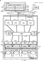
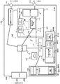
図1は、本実施形態に係る記憶制御システムを備えるコンピュータシステムの構成を示すブロック図である。 FIG. 1 is a block diagram illustrating a configuration of a computer system including a storage control system according to the present embodiment.
このコンピュータシステム1では、通信ネットワーク820に、1以上のホスト端末200と、記憶制御システム600とが接続されている。通信ネットワーク820は、ファイルレベルのデータがやり取りされる通信ネットワークであり、例えば、LAN、インターネット、専用回線、公衆回線等を場合に応じて適宜用いることができる。
In the
1以上のホスト端末200の各々は、例えば、CPU(Central Processing Unit)やメモリ等の情報処理資源を備えたコンピュータ装置であり、例えば、パーソナルコンピュータ、ワークステーション、メインフレーム等として構成される。ホスト端末200は、例えば、キーボードスイッチやポインティングデバイス、マイクロフォン等の情報入力装置(図示せず)と、例えば、モニタディスプレイやスピーカー等の情報出力装置(図示せず)とを備えている。さらに、ホスト端末200は、例えば、NASを利用するためのNAS利用ソフトウェア200Bと、Windows(登録商標)又はUNIX(登録商標)等のOS(オペレーティングシステム)200Cと、ネットワークドライバ200Fとを備える。ホスト端末200は、例えば、ファイル名を指定してファイル単位でのデータ入出力を記憶制御システム600に要求する。NAS用ソフトウェア200Bとしては、例えば、OS200CがUNIX(登録商標)の場合、NFS(Network
File System)であり、OS200CがWindows(登録商標)の場合、CIFS(Common Interface File System)である。また、ネットワークドライバ200Fには、例えば、TCP(Transmission
Control Protocol)に基づくデータ処理を行うTCPドライバ200Dと、IP(Internet Protocol)に基づくデータ処理を行うIPドライバ200Eとが含まれる。
Each of the one or
When the OS 200C is Windows (registered trademark), it is a CIFS (Common Interface File System). The
A TCP driver 200D that performs data processing based on (Control Protocol) and an IP driver 200E that performs data processing based on IP (Internet Protocol) are included.
記憶制御システム600は、例えば、アレイ状に配列された多数の物理記憶デバイス300を備えるRAIDシステムである。記憶制御システム600は、記憶制御装置100と記憶装置ユニット101とに大別することができる。記憶制御装置100は、例えば、複数のチャネルアダプタNAS(以下、「CHN」と略記)110と、複数のディスクアダプタ(以下、DKA)140と、キャッシュメモリ130と、共有メモリ120と、接続部150とを備えている。
The
CHN110は、ホスト端末200との間のデータ通信を行うものである。CHN110は、例えば、CPUやメモリ等を備えたマイクロコンピュータシステムとして構成されており、ホスト端末200から受信した各種コマンドを解釈して実行する。CHN110には、自分を識別するためのネットワークアドレス(例えば、IPアドレスやWWN)が割り当てられている。CHN110は、ホスト端末200から通信ネットワーク820を介してファイル単位でのI/O要求(例えば、ファイル名と、そのファイル名を持つファイルをリード又はライトする命令とを含んだコマンド、以下、「ファイルI/O要求」と言う)を受けて、そのファイルI/O要求を処理するNAS(Network Attached Storage)として振る舞うことができるようになっている。CHN110は、ホスト端末200から受信したデータをキャッシュメモリ130に格納したり、DKA140によってキャッシュメモリ130に格納されたデータを取得してホスト端末200に送信したりする。
The
DKA140は、記憶装置ユニット101内の論理的な記憶ユニット(以下、LU)310との間のデータ授受を行うものである。DKA140は、LU310を備える物理記憶デバイス300に接続するための図示しない通信ポートを備えている。また、DKA140は、CPUやメモリ等を備えたマイクロコンピュータシステムとして構成されている。DKA140は、CHN110からキャッシュメモリ130に書き込まれたデータを取得してLU310に書込んだり、また、LU310から読み出したデータをキャッシュメモリ130に格納したりする。DKA140は、LU310との間でデータ入出力を行う場合、論理的なアドレスを物理的なアドレスに変換する。
The
キャッシュメモリ(以下、「CM」と略記する場合有り)130は、例えば揮発性又は不揮発性のメモリであり、ホスト端末200から受信してLM310へ書き込まれるデータや、LU310から読出されてホスト端末200へ転送されるデータを一時的に記憶するものである。
The cache memory (hereinafter may be abbreviated as “CM”) 130 is, for example, a volatile or non-volatile memory. Data received from the
共有メモリ(以下、「SM」と略記する場合有り)120は、例えば不揮発性のメモリであり、ホスト端末との間でやり取りされるデータに関する制御情報(例えば、CM130上に確保されたどのキャッシュ領域にどのデータが格納されるべきかを示す情報)等が格納される。また、共有メモリ120には、例えば、ワーク領域(例えば、CHN110及びDKA140のCPU間でやり取りされるメッセージを一時的に記憶する領域)が設定される。なお、図示の例では、CM130とSM120は、物理的に分離しているが、一つのメモリであっても良い。その場合、そのメモリ上のメモリ空間が、論理的に、CM用の空間とSM用の空間とに分けられても良い。
The shared memory (hereinafter sometimes abbreviated as “SM”) 120 is, for example, a non-volatile memory, and control information regarding data exchanged with the host terminal (for example, which cache area secured on the CM 130) Information indicating which data should be stored in the storage area. In the shared memory 120, for example, a work area (for example, an area for temporarily storing messages exchanged between the CPUs of the
接続部150は、各CHN110、各DKA140、キャッシュメモリ130及び共有メモリ120を相互に接続させる。接続部150は、例えば、高速スイッチング動作によってデータ伝送を行う超高速クロスバスイッチ等のような高速バスとして構成することができる。
The
記憶装置ユニット101には、アレイ状に配列された複数の物理記憶デバイス300が含まれている。物理記憶デバイス300としては、例えば、ハードディスク、フレキシブルディスク、磁気テープ、半導体メモリ、光ディスク等のようなデバイスを用いることができる。物理記憶デバイス300の記憶領域上には、論理的な記憶デバイスである複数の論理ユニット(以下、「LU」と略記)310が備えられている。
The
以下、本実施形態についてより詳細に説明する。なお、以下の説明では、NAS用ソフトウェア200Bは、NFSであるとする。
Hereinafter, this embodiment will be described in more detail. In the following description, it is assumed that the
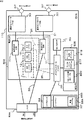
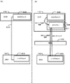
図2は、CHN110の構成例を示すブロック図である。
FIG. 2 is a block diagram illustrating a configuration example of the
CHN110は、複数(又は1つ)の通信ポート207と、2以上(又は1つ)の通信コントローラ/TOE503と、I/Oプロセッサ504及びI/Oメモリ507を備えた1つ(又は複数)の入出力制御部869と、メモリコントローラブリッジ505と、NASプロセッサ506と、NASメモリ508と、コネクタ509と、転送LSI502とを備えている。
The
通信コントローラ/TOE503は、通信コントローラとTOE(TCP/IPオフロードエンジン)とが一体になったハードウェア回路であり、通信ポート207及び転送LSI502に接続される。通信コントローラは、例えばLANコントローラであり、IPに基づくデータ処理を行う。TOEは、TCPに基づくデータ処理を行う。なお、通信コントローラとTOEは、物理的に分離していても良い。
The communication controller /
メモリコントローラブリッジ505は、NASプロセッサ506、NASメモリ508、I/Oプロセッサ504及び転送LSI502に接続されており、それらの間の通信を中継するLSI(Large-Scale Integrated circuit)である。メモリコントローラブリッジ505には、後述するメモリブリッジ転送バス31及びプロセッサレジスタバス35が接続される。
The
NASメモリ508は、NASプロセッサ506の制御を司るプログラムを記憶することができる。NASメモリ508は、例えば、ファイルシステムプログラム817、ネットワーク制御プログラム818、対応レジスタ管理テーブル820等を記憶することができる。ファイルシステムプログラム817は、例えば、ファイルI/O要求に含まれているファイル名と、そのファイル名を有するファイルが格納されている場所のアドレス情報(例えばLUN及び先頭論理ブロックアドレス)との対応づけを管理し、その対応付けに基づいて、ファイルI/O要求をブロックI/O要求に変換する。ネットワーク制御プログラム818は、例えば、NFS(Network File System)とSambaの2つのファイルシステムプロトコルを含んで構成される。NFSは、NFSが動作するUNIX(登録商標)オペレーティングシステムを搭載したホスト端末からのファイルI/O要求を受け付ける。一方、Sambaは、CIFS(Common
Interface File System)が動作するWindows(登録商標)オペレーティングシステムを搭載したホスト端末らのファイルI/O要求を受け付ける。対応レジスタ管理テーブル820には、複数の対応レジスタ12にそれぞれ対応した複数のレジスタID及び複数の使用状態データが登録されている。
The
A file I / O request is received from a host terminal equipped with a Windows (registered trademark) operating system that operates (Interface File System). In the corresponding register management table 820, a plurality of register IDs and a plurality of usage state data respectively corresponding to the plurality of
NASプロセッサ506は、例えばCPU又はマイクロプロセッサであり、メモリコントローラブリッジ505に接続されている。NASプロセッサ506は、NASメモリ508に格納されているファイルシステムプログラム817及びネットワーク制御プログラム818等を読出し、読み出したコンピュータプログラムに従う処理を実行することができる。例えば、NASプロセッサ506は、ネットワーク制御プログラム818により、ホスト端末200からのファイルI/O要求を受け付ける。また、NASプロセッサ506は、ファイルシステムプログラム817により、ホスト端末200から受信しNASメモリ508に格納されたファイルI/O要求をブロックI/O要求に変換してI/Oプロセッサ504に出力することができる(なお、ブロックとは、LU310上の記憶領域におけるデータの管理単位である)。また、NASプロセッサ506は、データ転送を伴うアクセス要求がホスト端末200から出力される場合、それに先行して、所定の先行コマンドをホスト端末200から受ける。その場合、NASプロセッサ506は、メモリコントローラブリッジ505及びプロセッサレジスタバス35を介して、複数の対応レジスタ12の中から選択された対応レジスタ12に、ファイルシステムアドレスを登録する。また、NASプロセッサ506は、上記選択された対応レジスタ12のレジスタIDを、I/Oプロセッサ504に通知する。
The
I/Oプロセッサ504は、例えばCPU又はマイクロプロセッサであり、I/Oメモリ507から読み出した制御プログラム864により、接続部150との間のデータの授受や、NASプロセッサ506と接続部150との間のデータ通信の中継や、キャッシュメモリ130上のキャッシュアドレスの管理等を実行することができる。また、I/Oプロセッサ504は、NASプロセッサ506からのブロックI/O要求に応答して、キャッシュメモリ130上にキャッシュ領域を確保すると共に、確保されたキャッシュ領域を表すキャッシュアドレスを、メモリコントローラブリッジ505及びプロセッサレジスタバス35を介して、NASプロセッサ506から通知されたレジスタIDに対応した対応レジスタ12に登録することができる。
The I /
I/Oメモリ507は、I/Oプロセッサ504の制御を司るコンピュータプログラム等を格納する。
The I /
コネクタ509は、接続部150に接続される。具体的には、例えば、コネクタ509は、接続部150に含まれるCM転送経路(CM130に接続された転送経路)及びSM転送経路(SM120に接続されて転送経路)に接続される。なお、必ずしも、一つのコネクタ509に、CM転送経路とSM転送経路とが混在する必要はない。例えば、コネクタ509の代わりに、CM転送経路に接続される第1のコネクタと、SM転送経路に接続される第2のコネクタとが備えられても良い。
The
転送LSI502は、例えば、通信コントローラ/TOE503、メモリコントローラブリッジ505、キャッシュメモリ130及び共有メモリ120の相互の通信を可能とするためのLSI(Large-Scale Integrated circuit)である。転送LSI502は、複数(又は1つ)の対応レジスタ12と、1以上(例えば通信コントローラ/TOE503と同数)の転送先判定回路11とを備えている。
The
複数の対応先レジスタ12の各々には、その対応先レジスタ12とプロセッサ504又は506との間でやり取りされるデータが経由するプロセッサレジスタバス35と、後述する判定レジスタバス34とが接続される。複数の対応レジスタ12の各々には、後に詳述するように、ファイルシステムアドレスと、そのファイルシステムアドレスに対応付けられたキャッシュアドレスとが登録される。なお、転送先LSI502に備えられる対応先レジスタ12の数は、例えば、CHN110が同時に受けることができるホスト端末200からのアクセス数と同数である。
A
転送先判定回路11は、例えば純粋なハードウェア回路である。転送先判定回路11には、複数の対応先レジスタ12に対するアクセス経路となる判定レジスタバス34と、コネクタ590を介してキャッシュメモリ130や共有メモリ120との間でやり取りされるデータが経由するコネクタ転送バス33と、メモリコントローラブリッジ505との間でやり取りされるデータが経由するメモリブリッジ転送バス35とが接続される。転送先判定回路11は、例えば、ホスト端末200から通信コントローラ/TOE503を介して受信したアクセス要求が、データ転送を伴うアクセス要求であるか否かを判別し、その判別の結果、データ転送を伴うアクセス要求であり、且つ、複数の対応レジスタ12の少なくとも1つからアクセス先キャッシュアドレスを認識できる場合には、認識されたアクセス先キャッシュアドレスとの間で、NASメモリ508を介すること無くダイレクトにデータ転送を行う。具体的には、例えば、転送先判定回路11は、ホスト端末200から通信コントローラ/TOE503を介してリード要求(例えば、「NFSPROC_READ」)を受信した場合、そのリード要求に含まれているファイルシステムアドレスを記憶した対応レジスタ12が存在するならば、その対応レジスタ12に記憶されているキャッシュアドレスが示すキャッシュ領域からコネクタ転送バス33を介してリード対象データを読出し、そのリード対象データを、NASメモリ508を介することなくダイレクトに通信コントローラ/TOE503を介してホスト装置200に転送する。また、例えば、転送先判定回路11は、ホスト端末200から通信コントローラ/TOE503を介してライト要求(例えば、「NFSPROC_WRITE」)を受信した場合、そのライト要求に含まれているファイルシステムアドレスを記憶した対応レジスタ12が存在するならば、そのライト要求が有するライト対象データを、その対応レジスタ12に記憶されているキャッシュアドレスが示すキャッシュ領域に、NASメモリ508を介することなくコネクタ転送バス33を介してダイレクトに転送する。
The transfer
以上が、CHN110の構成例である。なお、上述したプロセッサレジスタバス35、判定レジスタバス34及びメモリブリッジ転送バス31は、論理的なバスを示す。転送LSI502内の各構成要素とメモリコントローラブリッジ505とは、PCIバス等の物理的な単一バス(図示せず)で互いに接続される(この点は、後述の図7についても同様である)。
The configuration example of the
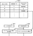
図3は、対応先レジスタ12の構成例を示す。
FIG. 3 shows a configuration example of the
図3に示すように、対応先レジスタ12には、ホスト端末200のNFS200Bから出力されるファイルシステムアドレスと、そのファイルシステムアドレスに対応付けられた1又は複数のキャッシュアドレスとが登録される。
As shown in FIG. 3, a file system address output from the
ファイルシステムアドレスとは、アクセス対象のデータファイル(例えば、ホスト端末200がLU310に対して入出力するユーザファイル)のアドレスに関する情報、例えば、アクセス対象のデータファイル中のどの場所からのどれぐらいの長さのデータのことを指すかを示す情報である。具体的には、例えば、ファイルシステムアドレスには、ファイルハンドルと、オフセットと、データ長とが含まれている。ファイルハンドルは、例えば、アクセス対象のデータファイルの先頭アドレスを表す。オフセットとは、ファイルハンドルからのオフセットのことであり、具体的には、アクセス対象のデータファイルにおける実際のアクセス対象先頭アドレスを表す。データ長とは、アクセス対象のデータファイルにおける上記オフセットからのデータ長のことであり、例えば、図示のように、データファイル30がMバイト単位でアクセス(書込み又は読込み)される場合には、データ長はMを表す。
The file system address is information related to the address of the data file to be accessed (for example, a user file input / output by the
1又は複数のキャッシュアドレスとは、キャッシュメモリ130上の記憶領域を示すアドレスのことであり、例えば、1つのファイルシステムアドレスに基づいてキャッシュメモリに書込まれる又は読み出されるデータサイズ分の記憶領域を表す。具体的には、例えば、キャッシュメモリ130がキャッシュブロック130S単位で管理されている場合、1つのキャッシュアドレスは1つのキャッシュブロック130Sを表し、キャッシュアドレスは、1つのファイルシステムアドレスに対してK(K≧1)個登録される。具体的には、例えば、データファイル30がMバイト(例えば4096バイト)単位でアクセスされ、キャッシュメモリ130上の各キャッシュブロック130Sの領域サイズがNバイト(例えば512バイト)の場合、キャッシュアドレスの数Kは、M÷Nの商の値(例えば4096/512=8)となる。なお、余りが生じた場合は、商の値に1が加えられてもよい。
One or a plurality of cache addresses is an address indicating a storage area on the
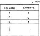
図4は、対応レジスタ管理テーブル820の構成例を示す。 FIG. 4 shows a configuration example of the corresponding register management table 820.
対応レジスタ管理テーブル820には、複数の対応レジスタ12にそれぞれ対応した複数のレジスタID及び複数の使用状態データが登録される。 In the correspondence register management table 820, a plurality of register IDs and a plurality of usage state data respectively corresponding to the plurality of correspondence registers 12 are registered.
レジスタIDとは、対応する対応レジスタの識別情報(例えば番号)である。 The register ID is identification information (for example, a number) of a corresponding register.
使用状態データとは、対応する対応レジスタ12の使用状態を示すデータであり、例えば、使用中か否かを示す情報(例えば、使用中であれば「1」であり、未使用であれば「0」)である。
The usage status data is data indicating the usage status of the corresponding corresponding
以下、本実施形態で行われるデータ転送処理流れの例を説明する。 Hereinafter, an example of the flow of data transfer processing performed in this embodiment will be described.
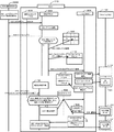
図5は、ホスト端末200のユーザがNFS200Bに対してファイルリードを要求した場合に行なわれる処理流れを示す。
FIG. 5 shows a processing flow performed when the user of the
ホスト端末200のNFS200Bは、ユーザからファイルリード要求を受けた場合(ステップS1)、要求されたファイル名を有するデータファイルを取得するためにどこにアクセスすれば良いかを要求する先行コマンドを送信する。具体的には、例えば、ホスト端末200のNFS200Bは、ファイルハンドラの要求(例えば「NFSPROC_LOOKUP」)を送信する(S2)。
When the
NASプロセッサ506は、ホスト端末200のNFS200Bから通信コントローラ/TOE503を介して受けたファイルハンドラ要求に従って、ファイルシステムプログラム817に基づくファイル処理を行う(S3)。そして、NASプロセッサ506は、そのファイル処理によって取得されたファイルハンドラ(受信したファイルハンドラ要求に対応したファイルハンドラ)を、ホスト端末200のNFS200Bに送信する(S4)。
The
また、NASプロセッサ506は、複数の対応レジスタ12の中から未使用の対応レジスタ12を探す(S5)。具体的には、NASプロセッサ506は、メモリコントローラブリッジ505を介して対応レジスタ管理テーブル820を参照し、対応レジスタ管理テーブル820に記録されている複数の使用状態データの中から未使用を示す使用状態データを探す。
Further, the
S5において、未使用の対応レジスタ12が探し出された場合(S5でY)、NASプロセッサ506は、探し出された未使用の対応レジスタ12を確保する(S6)。具体的には、NASプロセッサ506は、対応レジスタ管理テーブル820において、探し出された対応レジスタ12に対応する使用状態データを「未使用」から「使用中」に変更する。
If an unused
また、NASプロセッサ506は、S5でYの場合、上記取得されたファイルハンドラに基づくファイルシステムアドレスを、メモリコントローラブリッジ505及びプロセッサレジスタバス35を介して、S6で確保した対応レジスタ12に書込む(S7)。
In the case of Y in S5, the
また、NASプロセッサ506は、S5でYの場合、上記取得されたファイルハンドラに基づくファイルシステムアドレスを、LU310の記憶領域の管理単位であるブロックレベルのアドレスに変換し、そのブロックレベルのアドレスを有するリード要求(以下、ブロックリード要求)と、S6で確保された対応レジスタ12のレジスタIDとを、I/Oプロセッサ504に送信する(S8)。
Further, if the answer is Y in S5, the
I/Oプロセッサ504は、レジスタID及びブロックリード要求を受信した場合、ブロックリード要求に基づいて、キャッシュメモリ130上に、そのブロックリード要求に従って読み出すデータ(以下、リード対象データ)を格納するためのキャッシュ領域131を確保する(S9)。そして、I/Oプロセッサ504は、DKA140上の図示しないI/Oプロセッサとプロセッサ間通信を行うことにより、受信したブロックリード要求に含まれるアドレスが表す場所(LU310内の場所)からリード対象データを読み出し、そのリード対象データを、上記確保したキャッシュ領域131に格納する(S10)。
When the I /
また、I/Oプロセッサ504は、確保したキャッシュ領域131を表すK個のキャッシュアドレスを、メモリコントローラブリッジ505及びプロセッサレジスタバス35を介して、上記受信したレジスタIDに対応する対応レジスタ12に書込む(S11)。
Also, the I /
さて、ホスト端末200のNFS200Bは、S4の処理によってファイルハンドラを受信した場合、受信したファイルハンドラに基づくファイルシステムアドレスを含んだファイルリード要求を、CHN110に送信する(S12)。
When the
CHN110の転送先判定回路11は、ファイルシステムアドレスを含んだファイルリード要求を通信コントローラ/TOE503を介して受信する。受信したファイルリード要求は、通信コントローラ/TOE503において、既に、IP及びTCPに基づくデータ処理が行われている。
The transfer
転送先判定回路11は、受信したアクセス要求はキャッシュメモリ130へのデータ転送を伴うアクセス要求であり、且つ、そのアクセス要求に対応したキャッシュアドレスが複数の対応レジスタ12のいずれかに記録されているか否かを判断する(S13)。具体的には、例えば、転送先判定回路11は、受信したアクセス要求が「NFSPROC_READ」又は「NFSPROC_WRITE」であり、且つ、そのアクセス要求に含まれるファイルシステムアドレスを記憶する対応レジスタ12を複数の対応レジスタ12の中に存在するか否かを判断する。
The transfer
S13において、否定的な判断結果が得られた場合、すなわち、以下の(1)又は(2)の場合、
(1)受信したアクセス要求がキャッシュメモリ130へのデータ転送を伴うアクセス要求では無い(例えば「NFSPROC_READ」及び「NFSPROC_WRITE」のいずれでもない)と判断された場合、
(2)受信したアクセス要求がキャッシュメモリ130へのデータ転送を伴うアクセス要求(例えば「NFSPROC_READ」)であっても、受信したアクセス要求に含まれるファイルシステムアドレスを記憶する対応レジスタ12が複数の対応レジスタ12の中から見つからなかった場合、
転送先判定回路11は、NASプロセッサ506にデータ読出し指令を出力する。それにより、NASプロセッサ506からI/Oプロセッサ504に、ブロックリード要求が出力される。そして、そのブロックリード要求を受信したI/Oプロセッサ504によって、キャッシュメモリ130にステージングされているリード対象データが読み出されてNASメモリ508に格納され(S15及びS16)、NASプロセッサ506によって、NASメモリ508に格納されたリード対象データが読み出されて、ホスト端末200に転送される(S17及びS18)。
When a negative determination result is obtained in S13, that is, in the case of (1) or (2) below,
(1) When it is determined that the received access request is not an access request involving data transfer to the cache memory 130 (for example, neither “NFSPROC_READ” nor “NFSPROC_WRITE”)
(2) Even if the received access request is an access request involving data transfer to the cache memory 130 (for example, “NFSPROC_READ”), the corresponding
The transfer
一方、S13において、肯定的な判断結果が得られた場合、すなわち、受信したアクセス要求がキャッシュメモリ130へのデータ転送を伴うアクセス要求(例えば「NFSPROC_READ」)であり、且つ、受信したアクセス要求に含まれるファイルシステムアドレスを記憶する対応レジスタ12が複数の対応レジスタ12の中から見つかった場合、転送先判定回路11は、ダイレクトデータ転送処理を行う。具体的には、転送先判定回路11は、その見つかった対応レジスタ12に記憶されているK個のキャッシュアドレスを判定レジスタバス34を介して取得し、取得されたK個のキャッシュアドレスが示すキャッシュ領域131(例えばK個のキャッシュブロック130S)から、コネクタ転送バス33を経由してリード対象データを読み出し、読出したリード対象データを、NASメモリ508を介することなく通信コントローラ/TOE503を介してホスト端末200に転送する(S19)。
On the other hand, when a positive determination result is obtained in S13, that is, the received access request is an access request (for example, “NFSPROC_READ”) involving data transfer to the
以上が、ホスト端末200のユーザがNFS200Bに対してファイルリードを要求した場合に行なわれる処理流れである。なお、この処理流れにおいて、S4の処理は、S11の後に行われても良い。また、S12のファイルリード要求に含まれるファイルシステムアドレスは、例えば、転送先判定回路11によって、NASメモリ508に格納されても良いし、I/Oプロセッサ504によって、I/Oメモリ507に格納されても良い。
The above is the processing flow performed when the user of the
図6は、ホスト端末200のユーザがNFS200Bに対してファイルライトを要求した場合に行なわれる処理流れを示す。なお、以下の説明において、図5を参照して説明した部分と重複する部分については説明を省略或いは簡略する。
FIG. 6 shows a processing flow performed when the user of the
ホスト端末200のNFS200Bは、ユーザからファイルライト要求を受けた場合(ステップS21)、要求されたファイル名を有するデータファイルを書込むためにどこにアクセスすれば良いかを要求するためのファイルハンドラ要求を送信する(S22)。
When the
NASプロセッサ506は、受信したファイルハンドラ要求に従ってファイル処理を行い(S23)、そのファイル処理によって取得されたファイルハンドラを、ホスト端末200のNFS200Bに送信する(S24)。
The
また、NASプロセッサ506は、複数の対応レジスタ12の中から未使用の対応レジスタ12を探す(S25)。
Further, the
S25において、未使用の対応レジスタ12が探し出された場合(S25でY)、NASプロセッサ506は、探し出された未使用の対応レジスタ12を確保する(S26)。
If an unused
また、NASプロセッサ506は、S25でYの場合、上記取得されたファイルハンドラに基づくファイルシステムアドレスを、メモリコントローラブリッジ505及びプロセッサレジスタバス35を介して、S26で確保した対応レジスタ12に書込む(S27)。
If the answer is Y in S25, the
また、NASプロセッサ506は、S25でYの場合、上記取得されたファイルハンドラに基づくファイルシステムアドレスをブロックレベルのアドレスに変換し、そのブロックレベルのアドレスを有するライト要求(以下、ブロックライト要求)と、S26で確保された対応レジスタ12のレジスタIDとを、I/Oプロセッサ504に送信する(S28)。
In the case of Y in S25, the
I/Oプロセッサ504は、レジスタID及びブロックライト要求を受信した場合、ブロックライト要求に基づいて、キャッシュメモリ130上に、そのブロックライト要求に従って書込むデータ(以下、ライト対象データ)を格納するためのキャッシュ領域131を確保する(S29)。そして、I/Oプロセッサ504は、DKA140上の図示しないI/Oプロセッサとプロセッサ間通信を行うことにより、受信したブロックライト要求に含まれるアドレスが表す場所(LU310内の場所)から空データ(例えば全て「0」のビットから成るデータ)を読み出し、その空データを、上記確保したキャッシュ領域131に格納する(S30)。なお、このS30の処理は行わなくても良い。
When the I /
また、I/Oプロセッサ504は、確保したキャッシュ領域131を表すK個のキャッシュアドレスを、メモリコントローラブリッジ505及びプロセッサレジスタバス35を介して、上記受信したレジスタIDに対応する対応レジスタ12に書込む(S31)。
Also, the I /
さて、ホスト端末200のNFS200Bは、S24の処理によってファイルハンドラを受信した場合、受信したファイルハンドラに基づくファイルシステムアドレスを含んだファイルライト要求を、CHN110に送信する(S32)。
When the
CHN110の転送先判定回路11は、ファイルシステムアドレス及びライト対象データを含んだファイルライト要求を通信コントローラ/TOE503を介して受信する。転送先判定回路11は、受信したアクセス要求はキャッシュメモリ130へのデータ転送を伴うアクセス要求であり、且つ、そのアクセス要求に対応したキャッシュアドレスが複数の対応レジスタ12のいずれかに記録されているか否かを判断する(S33)。
The transfer
S33において、否定的な判断結果が得られた場合、転送先判定回路11は、NASプロセッサ506にデータ書込み指令を出力する(S34)。それにより、NASプロセッサ506によってNASメモリ508にライト対象データが書込まれ、且つ、NASプロセッサ506からブロックライト要求がI/Oプロセッサ504に出力される。そして、ブロックライト要求を受けたI/Oプロセッサ504によって、NASメモリ508に格納されているライト対象データが読み出されてキャッシュ領域131に格納される(S35及びS36)。
If a negative determination result is obtained in S33, the transfer
一方、S33において、肯定的な判断結果が得られた場合、すなわち、受信したアクセス要求がキャッシュメモリ130へのデータ転送を伴うアクセス要求(例えば「NFSPROC_WRITE」)であり、且つ、受信したアクセス要求に含まれるファイルシステムアドレスを記憶する対応レジスタ12が複数の対応レジスタ12の中から見つかった場合、転送先判定回路11は、ダイレクトデータ転送処理を行う。具体的には、転送先判定回路11は、その見つかった対応レジスタ12に記憶されているK個のキャッシュアドレスを判定レジスタバス34を介して取得し、取得されたK個のキャッシュアドレスが示すキャッシュ領域131(例えばK個のキャッシュブロック130S)に、NASメモリ508を介することなく、コネクタ転送バス33を経由してライト対象データを転送する(S37)。
On the other hand, when a positive determination result is obtained in S33, that is, the received access request is an access request (for example, “NFSPROC_WRITE”) involving data transfer to the
以上が、ホスト端末200のユーザがNFS200Bに対してファイルライトを要求した場合に行なわれる処理流れである。なお、この処理流れにおいて、S24の処理は、S31の後に行われても良い。また、S32のファイルライト要求に含まれるファイルシステムアドレスは、例えば、転送先判定回路11によって、NASメモリ508に格納されても良いし、I/Oプロセッサ504によって、I/Oメモリ507に格納されても良い。
The above is the processing flow performed when the user of the
以上、上述した実施形態によれば、データ転送を伴うアクセス要求がホスト端末200から発行されることに先行して、所定の先行コマンドがホスト端末200から発行される。CHN110において所定の先行コマンドが検出された場合、そのアクセス要求でやり取りされるデータのキャッシュ領域が確保されると共に、そのキャッシュ領域を表すキャッシュアドレスが対応レジスタ12上でファイルシステムに対応付けられる。また、ホスト端末200から出力されたアクセス要求は、ホスト端末200のTCPドライバ200D及びIPドライバ200EによってTCP及びIPに基づく処理が施されるが、そのアクセス要求のIP層及びTCP層の部分は、通信コントローラ/TOE503によって解釈されるので、転送先判定回路11が受信するアクセス要求は、NAS用ソフトウェア(例えばNFS)200Bから出力されたアクセス要求と同じものである。これらのことにより、ホスト端末200から、実際に、データ転送を伴うアクセス要求が発行された場合は、そのアクセス要求に従うデータは、そのアクセス要求に含まれるファイルシステムアドレスとそれに対応付けられたキャッシュアドレスとに基づいて、CHN110上のメモリを介することなく、ホスト端末200とキャッシュメモリ130との間で直接やり取りされる。これにより、ホスト端末200とキャッシュメモリ130との間のデータのやり取りが高速化される。これは、ホスト端末200から出力されたライト対象データをキャッシュメモリ130に転送する場合には特に効果的であると考えられる。また、これは、ホスト端末200とキャッシュメモリ130との間でやり取りされるデータが長くなればなるほど効果的であると考えられる。
As described above, according to the above-described embodiment, a predetermined preceding command is issued from the
また、上述した実施形態によれば、NASプロセッサ506が、ファイルレベルのI/O要求をブロックレベルのI/O要求に変換する仕様になっており、且つ、I/Oプロセッサ504が、キャッシュメモリ130を管理する(例えばキャッシュメモリ130上にキャッシュ領域を確保する)仕様になっている場合、それらの仕様を変更することなく、上述した高速化を実現することができる。
Further, according to the above-described embodiment, the
ところで、上述した実施形態について、例えば幾つかの変形例が考えられる。以下、各変形例について述べる。 By the way, some modifications can be considered about embodiment mentioned above, for example. Hereinafter, each modification will be described.
(1)第1の変形例。 (1) First modification.
図7は、本実施形態の第1の変形例におけるCHN110の構成例を示す。なお、以下の説明では、上述した実施形態の説明と重複する部分については説明を省略或いは簡略する。
FIG. 7 shows a configuration example of the
第1の変形例では、転送先判定回路11は、通信コントローラ/TOE3に搭載されている。また、この場合、通信コントローラ/TOE3において、IPやTCPの解釈或いは処理を行うIP/TCP部4は、転送先判定回路11の場所よりも上位の場所(つまりホスト端末側の場所)に搭載されている。通信コントローラ/TOE3がアクセス要求を受信した場合に、IP及びTCPの解釈をした後のアクセス要求が転送先判定回路11に受信されるようにするためである。
In the first modification, the transfer
この第1の変形例では、上述した実施形態と同様に、転送先判定回路11に、メモリブリッジ転送バス31や、判定レジスタバス34を接続することができる。また、コネクタ転送バス33を介して、転送LSI5と転送先判定回路11とを接続することができる。この場合、例えば、転送先判定回路11からダイレクトデータ転送処理により出力されたライト対象データは、コネクタ転送バス33及びデータ転送LSI5を介して、キャッシュメモリ130に転送される。
In the first modification, the memory
(2)第2の変形例
図8は、本実施形態の第2の変形例における、CHN110とDKA140との間のデータ通信例を示す。
(2) Second Modification FIG. 8 shows a data communication example between the
第2の変形例では、CHN110には、I/Oプロセッサは搭載されず、CHN110内のI/Oプロセッサ504が行う処理を、DKA140のI/Oプロセッサ603に行わせる。
In the second modification, the
例えば、図8(A)に示すように、CHN110とDKA140との間に、専用の割込み線510が備えられる。この場合、NASプロセッサ506から出力されたブロックレベルのI/O要求は、専用の割込み線510を介して、DKA140のI/Oプロセッサ603に送信される。これにより、DKA140のI/Oプロセッサ603によって、例えば、図5のS9〜S11の処理や、図6のS29〜S31の処理が行われる。
For example, as shown in FIG. 8A, a dedicated interrupt
また、例えば、図8(B)に示すように、CHN110上のNASメモリ508に、コマンドキュー511が設けられる。NASプロセッサ506から出力されたブロックレベルのI/O要求は、そのコマンドキュー511に格納される(S51)。DKA140のI/Oプロセッサ603は、コマンドキューをポーリングし(S52)、I/O要求が存在することを検出した場合には、そのI/O要求をコマンドキューから取得する(S53)。
For example, as shown in FIG. 8B, a
(3)第3の変形例。 (3) Third modification.
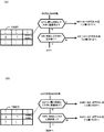
図9は、本実施形態の第3の変形例に係る対応レジスタ管理テーブル1820の構成例を示す。 FIG. 9 shows a configuration example of the corresponding register management table 1820 according to the third modification of the present embodiment.
対応レジスタ管理テーブル820には、各対応レジスタ毎に、更に、ファイルシステムアドレスのアドレス登録領域が存在する。各対応レジスタに対応したアドレス登録領域には、その対応レジスタに読み出されるデータのファイルシステムアドレスが登録される。 The corresponding register management table 820 further includes an address registration area for a file system address for each corresponding register. In the address registration area corresponding to each corresponding register, the file system address of the data read to the corresponding register is registered.
例えば、I/Oプロセッサ504は、図5のS11の後に、キャッシュアドレスの書込みが済んだことをNASプロセッサ506に通知する(S11A)。NASプロセッサ506は、その通知を受けた場合、S6で確保された対応レジスタ12に対応する対応レジスタ管理テーブル820上のアドレス登録領域に、S7で書き込んだファイルシステムアドレスを書込む(11B)。これにより、そのファイルシステムアドレスに対応するデータを記憶するキャッシュ領域130のキャッシュアドレスが登録済みの対応レジスタ12がどれであるかがわかるようになる。
For example, the I /
このような処理を行っておくことで、以後、ファイルハンドラ要求に応答してファイルハンドラが取得された場合には、そのファイルハンドラに基づくファイルシステムアドレスに対応したキャッシュアドレスが既に登録されている対応レジスタ12が存在するか否かの判定(以下、「登録判定処理」)を実行することができる。なお、S11Bの処理は、例えば、S7の際に行なわれても良い。
By performing such processing, if a file handler is acquired in response to a file handler request, a cache address corresponding to the file system address based on that file handler has already been registered. A determination as to whether or not the
図10は、この第3の変形例に係る登録判定処理が行われるタイミングの例を示す。 FIG. 10 shows an example of timing when the registration determination process according to the third modification is performed.
図10(A)は、リードの場合の例である。すなわち、例えば、図5のS3又はS4の後に、NASプロセッサ506は、登録判定処理を実行する(S4A)。具体的には、例えば、NASプロセッサ506は、取得されたファイルハンドラに基づくファイルシステムアドレスと同一のファイルシステムアドレスが対応レジスタ管理テーブル1820に存在するか否かを判断する。その結果、その同一のファイルシステムアドレスが対応レジスタ管理テーブル1820から見つからない場合(S4AでN)、上述したS5が行われる。一方、S4Aで、同一のファイルシステムアドレスが対応レジスタ管理テーブル1820から見つかった場合(S4AでY)、S5〜11が行われることなくS12が実行される。
FIG. 10A shows an example of a lead. That is, for example, after S3 or S4 in FIG. 5, the
図10(B)は、ライトの場合の例である。すなわち、例えば、図6のS23又はS24の後に、NASプロセッサ506は、登録判定処理を実行する(S24A)。その結果、取得されたファイルハンドラに基づくファイルシステムアドレスと同一のファイルシステムアドレスが対応レジスタ管理テーブル1820から見つからない場合(S24AでN)、上述したS25が行われる。一方、S24Aで、上記同一のファイルシステムアドレスが対応レジスタ管理テーブル1820から見つかった場合(S24AでY)、S25〜31が行われることなくS32が実行される。
FIG. 10B shows an example in the case of writing. That is, for example, after S23 or S24 in FIG. 6, the
ホスト端末200から、同一のファイルリード要求が連続して発行される場合がある。また、ホスト端末200から発行されるファイルライト要求に含まれるライト対象データは、過去にファイルリード要求を発行することによって読み出されたデータである場合がある。それらの場合、既に、図5に示した処理流れによって、ファイルリード要求或いはファイルライト要求に含まれるファイルシステムアドレスに対応したキャッシュアドレスが既に登録された対応レジスタ12が存在することになる。このような場合に、わざわざ、図5のS6〜S11の処理や、図6のS26〜S31の処理が行われるのは無駄である。上述した第3の変形例によれば、その無駄を防ぐことができる。
The same file read request may be issued continuously from the
以上、本発明の実施形態及び変形例を説明したが、これらは本発明の説明のための例示であって、本発明の範囲をこの実施形態及び変形例にのみ限定する趣旨ではない。本発明は、他の種々の形態でも実施することが可能である。例えば、CHN110とDKA140は一体に作られていても良い。また、例えば、複数の対応レジスタ12に代えて、同一のメモリ上で、複数のファイルシステムアドレスと、複数のファイルシステムアドレスの各々に対応するK個のキャッシュアドレスとが記録されても良い。
As mentioned above, although embodiment and the modification of this invention were demonstrated, these are the illustrations for description of this invention, Comprising: It is not the meaning which limits the scope of the present invention only to this embodiment and modification. The present invention can be implemented in various other forms. For example, the
100…記憶制御装置 101…記憶装置ユニット 103…データベース 104…データファイル 110…チャネルアダプタNAS(CHN) 120…共有メモリ 130…キャッシュメモリ 140…ディスクアダプタ 150…接続部 200…ホスト端末 200B…NAS用ソフトウェア 200C…OS 200D…TCPドライバ 200E…IPドライバ 200F…ネットワークドライバ 310…論理ユニット 600…記憶制御システム
DESCRIPTION OF
Claims (7)
外部装置と前記記憶デバイスとの間でやり取りされるデータが格納されるキャッシュ領域を有するキャッシュメモリと、
外部装置からデータを受信して前記キャッシュ領域に格納したり、前記キャッシュ領域に格納されているデータを読み出して前記外部装置に転送したりするチャネル制御部と、
前記キャッシュ領域に格納されているデータを読出して前記記憶デバイスに格納したり、前記記憶デバイスから読出したデータを前記キャッシュ領域に格納したりする記憶デバイス制御部と
を備え、
前記チャネル制御部は、
前記外部装置から受信したデータを記憶することができるデータ記憶メモリと、
データファイル中のデータのファイルレベルのアドレスであるファイルシステムアドレスと、前記ファイルシステムアドレスに対応付けられたキャッシュアドレスとを記憶する対応メモリと、
前記外部装置から受信したアクセス要求が、ファイルシステムアドレスを有するファイルアクセス要求である場合、前記ファイルアクセス要求に含まれるファイルシステムアドレスに対応付けられたキャッシュアドレスが前記対応メモリから識別されたならば、前記識別されたキャッシュアドレスが表すキャッシュ領域であるターゲットキャッシュ領域内のアクセス対象データを、前記データ記憶メモリを経由することなく前記外部装置に転送する、又は、前記ファイルアクセス要求が有するアクセス対象データを、前記データ記憶メモリを経由することなく前記ターゲットキャッシュ領域に転送する転送先判定回路と
を備える、
記憶制御システム。 A storage device for storing data;
A cache memory having a cache area for storing data exchanged between an external device and the storage device;
A channel control unit that receives data from an external device and stores the data in the cache region, or reads data stored in the cache region and transfers the data to the external device;
A storage device control unit that reads data stored in the cache area and stores the data in the storage device, or stores data read from the storage device in the cache area;
The channel controller
A data storage memory capable of storing data received from the external device;
A corresponding memory for storing a file system address which is a file level address of data in the data file, and a cache address associated with the file system address;
When the access request received from the external device is a file access request having a file system address, if the cache address associated with the file system address included in the file access request is identified from the corresponding memory, The access target data in the target cache area that is the cache area represented by the identified cache address is transferred to the external device without going through the data storage memory, or the access target data included in the file access request is A transfer destination determination circuit that transfers to the target cache area without going through the data storage memory,
Memory control system.
前記チャネル制御部及び前記記憶デバイス制御部の少なくとも一方が、前記変換されたブロックレベルのアドレスに基づいて、前記キャッシュメモリ上に前記キャッシュ領域を確保する第2のプロセッサを備え、
前記第1のプロセッサが、前記ファイルアクセス要求が発行されることに先行して前記外部装置から先行コマンドを受信し、前記先行コマンドに応答して、アクセス対象となるファイルシステムアドレスを前記対応メモリに書込み、前記ファイルシステムアドレスを前記ブロックレベルのアドレスに変換し、
前記第2のプロセッサが、前記第1のプロセッサによって変換された前記ブロックレベルのアドレスに基づいて、前記キャッシュ領域を確保し、前記確保したキャッシュ領域を表すキャッシュアドレスを、前記ファイルシステムアドレスが書き込まれた前記対応メモリに書込む、
請求項1記載の記憶制御システム。 The channel control unit further includes a first processor that converts the file system address into a block level address that is a management unit of a storage area of the storage device,
At least one of the channel control unit and the storage device control unit includes a second processor that secures the cache area on the cache memory based on the converted block level address;
The first processor receives a preceding command from the external device prior to the file access request being issued, and responds to the preceding command with a file system address to be accessed in the corresponding memory. Write, convert the file system address to the block level address,
The second processor secures the cache area based on the block-level address converted by the first processor, and the file system address is written in the cache address representing the secured cache area. Write to the corresponding memory,
The storage control system according to claim 1.
請求項1記載の記憶制御システム。 The channel control unit includes an IP circuit that interprets an Internet protocol for an access request received from the external device, and a transmission control protocol for an access request received from the external device, closer to the external device than the transfer destination determination circuit. The access request is input from the external device to the transfer destination determination circuit via the IP circuit and the TCP circuit.
The storage control system according to claim 1.
前記複数のレジスタの各々には、1つのファイルアクセス要求に含まれる1つのファイルシステムアドレスと、そのファイルシステムアドレスに対応付けられた1又は複数のキャッシュアドレスとが記憶される、
請求項1記載の記憶制御システム。 The corresponding memory is a plurality of registers,
Each of the plurality of registers stores one file system address included in one file access request and one or more cache addresses associated with the file system address.
The storage control system according to claim 1.
前記外部装置から受信したデータを記憶することができるデータ記憶メモリと、
前記外部装置からアクセス要求を受信した場合、前記アクセス要求が、前記外部装置と前記キャッシュ領域との間で行われるデータ転送を伴うデータアクセス要求であり、前記データアクセス要求に含まれる情報要素に対応付けられたキャッシュアドレスが識別されたならば、前記識別されたキャッシュアドレスが表すキャッシュ領域であるターゲットキャッシュ領域内のアクセス対象データを、前記データ記憶メモリを経由することなく前記外部装置に転送する、又は、前記アクセス要求に含まれるアクセス対象データを、前記データ記憶メモリを経由することなく前記ターゲットキャッシュ領域に転送する転送先判定回路と
を備えるチャネル制御装置。 A storage device for storing data, a cache memory having a cache area for storing data exchanged between the external device and the storage device, and receiving data from the external device and storing it in the cache area, A channel control device that reads data stored in the cache area and transfers it to the external device, and reads data stored in the cache area and stores it in the storage device, or reads from the storage device The channel control device installed in a storage control system comprising a storage device control unit that stores the stored data in the cache area,
A data storage memory capable of storing data received from the external device;
When an access request is received from the external device, the access request is a data access request involving data transfer performed between the external device and the cache area, and corresponds to an information element included in the data access request If the attached cache address is identified, the access target data in the target cache area, which is the cache area represented by the identified cache address, is transferred to the external device without going through the data storage memory. Alternatively, a channel control device comprising: a transfer destination determination circuit that transfers access target data included in the access request to the target cache area without going through the data storage memory.
前記転送先判定回路は、前記外部装置から受信したアクセス要求が、ファイルシステムアドレスを有するファイルアクセス要求である場合、前記ファイルアクセス要求に含まれるファイルシステムアドレスに対応付けられたキャッシュアドレスが前記対応メモリから識別されたならば、前記識別されたキャッシュアドレスが表すキャッシュ領域であるターゲットキャッシュ領域内のアクセス対象データを、前記データ記憶メモリを経由することなく前記ホスト端末に転送する、又は、前記ファイルアクセス要求が有するアクセス対象データを、前記データ記憶メモリを経由することなく前記ターゲットキャッシュ領域に転送する、
請求項5記載のチャネル制御装置。 A corresponding memory for storing a file system address, which is a file level address of data in the data file, and a cache address associated with the file system address;
When the access request received from the external device is a file access request having a file system address, the transfer destination determination circuit has a cache address associated with the file system address included in the file access request as the corresponding memory. If the access target data in the target cache area which is the cache area represented by the identified cache address is transferred to the host terminal without going through the data storage memory, or the file access Transferring access target data included in the request to the target cache area without going through the data storage memory;
The channel control apparatus according to claim 5.
前記データ転送装置の上位に存在する外部装置から受信したアクセス要求が、前記外部装置と、前記データ転送装置の下位に存在する下位記憶装置の記憶領域との間で行われるデータ転送を伴うデータアクセス要求であり、前記データアクセス要求に含まれる情報要素に対応付けられた記憶アドレスが識別されたならば、前記識別された記憶アドレスが表す記憶領域であるターゲット記憶領域内のアクセス対象データを、前記通信装置内のデータ記憶メモリを経由することなく前記外部装置に転送する、又は、前記アクセス要求に含まれるアクセス対象データを、前記データ記憶メモリを経由することなく前記ターゲット記憶領域に転送する転送先判定回路を備えたデータ転送装置。 In a data transfer device that can be installed in a communication device,
Data access involving data transfer in which an access request received from an external device existing above the data transfer device is performed between the external device and a storage area of a lower storage device existing lower than the data transfer device If the storage address associated with the information element included in the data access request is identified, the access target data in the target storage area that is the storage area represented by the identified storage address is Transfer destination to transfer to the external device without going through the data storage memory in the communication device, or to transfer the access target data included in the access request to the target storage area without going through the data storage memory A data transfer device including a determination circuit.
Priority Applications (2)
| Application Number | Priority Date | Filing Date | Title |
|---|---|---|---|
| JP2004111096A JP2005293478A (en) | 2004-04-05 | 2004-04-05 | Storage control system, channel control device provided in storage control system, data transfer device |
| US10/857,908 US7003553B2 (en) | 2004-04-05 | 2004-06-02 | Storage control system with channel control device having data storage memory and transfer destination circuit which transfers data for accessing target cache area without passing through data storage memory |
Applications Claiming Priority (1)
| Application Number | Priority Date | Filing Date | Title |
|---|---|---|---|
| JP2004111096A JP2005293478A (en) | 2004-04-05 | 2004-04-05 | Storage control system, channel control device provided in storage control system, data transfer device |
Publications (1)
| Publication Number | Publication Date |
|---|---|
| JP2005293478A true JP2005293478A (en) | 2005-10-20 |
Family
ID=35055717
Family Applications (1)
| Application Number | Title | Priority Date | Filing Date |
|---|---|---|---|
| JP2004111096A Pending JP2005293478A (en) | 2004-04-05 | 2004-04-05 | Storage control system, channel control device provided in storage control system, data transfer device |
Country Status (2)
| Country | Link |
|---|---|
| US (1) | US7003553B2 (en) |
| JP (1) | JP2005293478A (en) |
Cited By (1)
| Publication number | Priority date | Publication date | Assignee | Title |
|---|---|---|---|---|
| CN112905550A (en) * | 2021-03-25 | 2021-06-04 | 武汉悦学帮网络技术有限公司 | Data export method and device |
Families Citing this family (9)
| Publication number | Priority date | Publication date | Assignee | Title |
|---|---|---|---|---|
| CN1333346C (en) * | 2004-12-24 | 2007-08-22 | 北京中星微电子有限公司 | Method for accessing files |
| US9104315B2 (en) | 2005-02-04 | 2015-08-11 | Sandisk Technologies Inc. | Systems and methods for a mass data storage system having a file-based interface to a host and a non-file-based interface to secondary storage |
| US7627733B2 (en) * | 2005-08-03 | 2009-12-01 | Sandisk Corporation | Method and system for dual mode access for storage devices |
| JP2007102314A (en) * | 2005-09-30 | 2007-04-19 | Fujitsu Ltd | Disk cache controller |
| US7747837B2 (en) | 2005-12-21 | 2010-06-29 | Sandisk Corporation | Method and system for accessing non-volatile storage devices |
| US7793068B2 (en) * | 2005-12-21 | 2010-09-07 | Sandisk Corporation | Dual mode access for non-volatile storage devices |
| US7769978B2 (en) | 2005-12-21 | 2010-08-03 | Sandisk Corporation | Method and system for accessing non-volatile storage devices |
| CN109634876A (en) * | 2018-12-11 | 2019-04-16 | 广东省新代通信与网络创新研究院 | File access method, device and computer readable storage medium |
| CN119782209A (en) * | 2025-03-10 | 2025-04-08 | 济南浪潮数据技术有限公司 | Data storage method, system, computing device and electronic device |
Family Cites Families (10)
| Publication number | Priority date | Publication date | Assignee | Title |
|---|---|---|---|---|
| JP3136036B2 (en) | 1993-11-16 | 2001-02-19 | 富士通株式会社 | Control method of disk controller |
| JP3790323B2 (en) * | 1997-04-16 | 2006-06-28 | 株式会社ルネサステクノロジ | Data transfer control device, microcomputer and data processing system |
| US6311252B1 (en) | 1997-06-30 | 2001-10-30 | Emc Corporation | Method and apparatus for moving data between storage levels of a hierarchically arranged data storage system |
| US6757291B1 (en) * | 2000-02-10 | 2004-06-29 | Simpletech, Inc. | System for bypassing a server to achieve higher throughput between data network and data storage system |
| JP2003140837A (en) | 2001-10-30 | 2003-05-16 | Hitachi Ltd | Disk array controller |
| JP2003162439A (en) * | 2001-11-22 | 2003-06-06 | Hitachi Ltd | Storage system and control method thereof |
| JP2003316713A (en) * | 2002-04-26 | 2003-11-07 | Hitachi Ltd | Storage system |
| JP2004110503A (en) | 2002-09-19 | 2004-04-08 | Hitachi Ltd | Storage control device, storage system, control method for storage control device, channel control unit, and program |
| US20050177641A1 (en) * | 2004-01-16 | 2005-08-11 | Hitachi, Ltd. | Method and apparatus for limiting access to a storage system |
| US20050210028A1 (en) * | 2004-03-18 | 2005-09-22 | Shoji Kodama | Data write protection in a storage area network and network attached storage mixed environment |
-
2004
- 2004-04-05 JP JP2004111096A patent/JP2005293478A/en active Pending
- 2004-06-02 US US10/857,908 patent/US7003553B2/en not_active Expired - Lifetime
Cited By (1)
| Publication number | Priority date | Publication date | Assignee | Title |
|---|---|---|---|---|
| CN112905550A (en) * | 2021-03-25 | 2021-06-04 | 武汉悦学帮网络技术有限公司 | Data export method and device |
Also Published As
| Publication number | Publication date |
|---|---|
| US20050223166A1 (en) | 2005-10-06 |
| US7003553B2 (en) | 2006-02-21 |
Similar Documents
| Publication | Publication Date | Title |
|---|---|---|
| EP1571542B1 (en) | Storage control system and method | |
| JP3997061B2 (en) | Storage subsystem and storage subsystem control method | |
| US9513825B2 (en) | Storage system having a channel control function using a plurality of processors | |
| JP4686463B2 (en) | Storage shelf router interface tunneling system and method | |
| EP1837751B1 (en) | Storage system, storage extent release method and storage apparatus | |
| US8296468B2 (en) | Storage controller and controlling method therefor | |
| JP4871880B2 (en) | Storage shelf router integrated circuit | |
| JP2007207007A (en) | Storage system, storage controller and computer system | |
| JP2004220216A (en) | SAN / NAS integrated storage device | |
| JP6068676B2 (en) | Computer system and computer system control method | |
| JP2004199420A (en) | Computer system, magnetic disk device, and disk cache control method | |
| JP4285058B2 (en) | Network management program, management computer and management method | |
| JP4497957B2 (en) | Storage control system | |
| JP2005165852A (en) | Storage system, storage control device, and storage system control method | |
| US20160224369A1 (en) | Zoning data to a virtual machine | |
| US7426588B2 (en) | Storage apparatus | |
| JP2005293478A (en) | Storage control system, channel control device provided in storage control system, data transfer device | |
| JP2005293370A (en) | Storage control system | |
| EP1768015A1 (en) | Storage unit and disk control method | |
| CN110515536B (en) | data storage system | |
| JP2006072440A (en) | Storage apparatus and data migration method thereof | |
| US20060242258A1 (en) | File sharing system, file sharing program, management server and client terminal | |
| US20140136581A1 (en) | Storage system and control method for storage system | |
| JP2007004710A (en) | Storage access system, data transfer device, storage accessing method and program | |
| JP2003058487A (en) | Data access control method |