JP2005293460A - Non-contact IC card inlet and non-contact IC card - Google Patents
Non-contact IC card inlet and non-contact IC card Download PDFInfo
- Publication number
- JP2005293460A JP2005293460A JP2004110930A JP2004110930A JP2005293460A JP 2005293460 A JP2005293460 A JP 2005293460A JP 2004110930 A JP2004110930 A JP 2004110930A JP 2004110930 A JP2004110930 A JP 2004110930A JP 2005293460 A JP2005293460 A JP 2005293460A
- Authority
- JP
- Japan
- Prior art keywords
- chip
- card
- contact
- antenna substrate
- inlet
- Prior art date
- Legal status (The legal status is an assumption and is not a legal conclusion. Google has not performed a legal analysis and makes no representation as to the accuracy of the status listed.)
- Pending
Links
Images

Landscapes
- Credit Cards Or The Like (AREA)
Abstract
【課題】 カードの厚み増加を抑制しつつ、点圧や鋼球落下等の衝撃に対して強く、カード表面の平坦性も良好な非接触ICカード用インレットを提供すること。
【解決手段】 アンテナ基板1のコイルアンテナの電極1aに対してICチップ2がフェースダウンで電気的に接合された非接触ICカード用インレットにおいて、アンテナ基板1の電極のパターンは、電極間の溝1bの形状がICチップ2の存在領域内で少なくとも一方向に沿っては直線的見通し不可の折り曲げ状態に形成されている。アンテナ基板1におけるコイルアンテナの電極1aのパターンの形状の変更をもって補強板の役目をさせる。
【選択図】 図1PROBLEM TO BE SOLVED: To provide an inlet for a non-contact IC card which is resistant to impacts such as a point pressure and a steel ball drop while suppressing an increase in card thickness and has a good card surface flatness.
In an inlet for a non-contact IC card in which an IC chip 2 is electrically connected face-down to an electrode 1a of a coil antenna of an antenna substrate 1, the electrode pattern of the antenna substrate 1 is a groove between the electrodes. The shape of 1b is formed in a bent state in which linear visibility is impossible along at least one direction in the region where the IC chip 2 exists. By changing the pattern shape of the electrode 1a of the coil antenna on the antenna substrate 1, the role of the reinforcing plate is made.
[Selection] Figure 1
Description
本発明は、非接触ICカードに内蔵されるものであって、コイルアンテナおよび電極を有するアンテナ基板と、前記アンテナ基板の前記電極に対してフェースダウンで電気的に接合されたICチップとを備えたインレットに関する。また、そのインレットを内蔵した非接触ICカードに関する。非接触ICカードは、内側のシート部分であるインレットと外側のシート部分であるオーバーレイからなるが、インレットはICモジュールにコイルアンテナを接続したものである。 The present invention is built in a non-contact IC card, and includes an antenna substrate having a coil antenna and an electrode, and an IC chip electrically connected face-down to the electrode of the antenna substrate. Related to the inlet. The present invention also relates to a non-contact IC card having the inlet built therein. The non-contact IC card includes an inlet that is an inner sheet portion and an overlay that is an outer sheet portion. The inlet is obtained by connecting a coil antenna to an IC module.
近年、コイルアンテナとICチップを内蔵し、電波により非接触で外部機器との間でデータ交換を行う非接触ICカードの開発が進んでいる。この非接触ICカードは、記憶容量の大きさと高度なセキュリティ機能を有するという特徴に加えて、外部機器に近づけるだけで通信が可能であるという特徴を有している。つまり、接触式カードのようにいちいちカードを出し入れするといった手間が不要であり、接点等の機構が不要でメンテナンスフリーを実現できる。その結果、非接触ICカードは、今後、より広範囲な分野への普及が予想される。 In recent years, development of a non-contact IC card that incorporates a coil antenna and an IC chip and exchanges data with an external device in a non-contact manner using radio waves has been progressing. This non-contact IC card has the feature that communication is possible only by bringing it close to an external device in addition to the feature of having a large storage capacity and an advanced security function. That is, it is not necessary to insert and remove cards one by one like a contact type card, and a mechanism such as a contact is not required and maintenance-free can be realized. As a result, non-contact IC cards are expected to spread to a wider range of fields in the future.
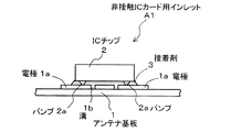
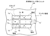
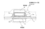
図10は従来の非接触ICカード用インレットの構成例を示すための要部の平面図、図11はその断面図である。これらの図において、A4は非接触ICカード用インレット、1はコイルアンテナ(図示せず)を形成したフィルム状のアンテナ基板、1aはアンテナ基板1におけるコイルアンテナの電極、1a′は電極パターンを形成する金属部分、2はICチップ、2aは金のバンプ、3は接着剤である。電極パターンを形成する金属部分1a′は、電極1aと同じ金属で形成されている。
FIG. 10 is a plan view of a main part for illustrating a configuration example of a conventional non-contact IC card inlet, and FIG. 11 is a cross-sectional view thereof. In these drawings, A4 is a contactless IC card inlet, 1 is a film-like antenna substrate on which a coil antenna (not shown) is formed, 1a is an electrode of a coil antenna on the
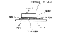
従来の非接触ICカード用インレットA4は、アンテナ基板1の上にICチップ2がボンディングされた構成となっている。ICチップ2がフェースダウンされ、その表面の端子部のバンプ2aがアンテナ基板1上のコイルアンテナの電極1aに電気的に接合されている。アンテナ基板1に対してICチップ2の固定を行う接着剤3としては、従来、ACF(Anisotropic Conductive Film:異方性導電フィルム)が一般的であったが、最近では、材料の効率的な使用の観点からACP(AnisotropicConductive Paste:異方性導電ペースト)やNCP(Non Conductive Paste:非導電ペースト)等の樹脂が使用されるようになっている。
The conventional non-contact IC card inlet A4 has a configuration in which an
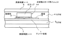
図12は、上記構成のインレットA4を内蔵する非接触ICカードの構成例を示す。コア材4において、そのICチップ実装部をくりぬいてインレットA4を装填し、必要に応じてインレット裏面にコア材5を接合し、さらに表裏両面にオーバーレイの表面保護シート6,7をラミネート加工している。
FIG. 12 shows a configuration example of a non-contact IC card incorporating the inlet A4 having the above configuration. In the
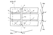
従来の非接触ICカードにおいては、アンテナ基板1上における電極1aのパターンについて、金属部分でない溝1bが、ICチップ2の存在領域内で端から端まで見通せる直線状に形成されている。しかし、この直線状の溝1bの存在のために、次のような強度上の問題が生じる。これを図13を用いて説明する。
In a conventional non-contact IC card, a
溝1bがICチップ2の存在領域に交わる一方の入口a,b,cから他方の出口a′,b′,c′に向かう線がそれぞれ直線状に見通せる状態となっている。a−a′の直線状の溝1bは、ICチップ2の存在領域でMaで示すようなアンテナ基板1の折れ曲がりの原因となる。また、b−b′の直線状の溝1bは、ICチップ2の存在領域でMbで示すようなアンテナ基板1の折れ曲がりの原因となり、c−c′の直線状の溝1bは、ICチップ2の存在領域でMcで示すようなアンテナ基板1の折れ曲がりの原因となる。なお、折れ曲がりMa,Mb,Mcは断面図となっている。
The
すなわち、ICカードの表面(ICチップ2の裏面)に鋼球落下試験のような衝撃的な応力がかかると、直線状の溝1bを折り曲げの稜線とする状態で、アンテナ基板1に折り曲げ力がかかる。その結果、溝1bの部分でアンテナ基板1が伸び、ICチップ2の表面に応力がかかって、ICチップ2が破損し、データがすべて失われてしまうおそれがある。したがって、折り曲げや衝撃等からICチップ2を保護するために、機械的強度を上げる必要がある。
That is, when an impact stress such as a steel ball drop test is applied to the front surface of the IC card (the back surface of the IC chip 2), the bending force is applied to the
ところが、一方で、非接触ICカードは、規格によりその厚みが決められている(例えば、ISO14443では、0.76mm±0.08mm)。そのため、単に厚みを増すことで機械的強度を上げるといった構成は、その採用がむずかしい。 However, on the other hand, the thickness of the non-contact IC card is determined by the standard (for example, ISO 14443, 0.76 mm ± 0.08 mm). Therefore, it is difficult to adopt a configuration in which the mechanical strength is simply increased by increasing the thickness.
従来の構成では、カードの裏面(ICチップの表面)からの点圧強度試験に耐えるように、カードの裏面(ICチップの表面)側に補強板を取り付ける方法が提案されている(例えば、特許文献1参照)。この補強板は、カード裏面(チップ表面)からの点圧強度試験に強い構成であるが、カードの表面(ICチップの裏面)からの鋼球落下試験に弱いことが当社の研究で判明している。また上記文献では、カード表面(ICチップ裏面)からの点圧強度試験に耐えるようにICチップ裏面にも補強板を取り付け、両面補強板の構成をとっている。 In the conventional configuration, a method has been proposed in which a reinforcing plate is attached to the back surface (IC chip surface) side of the card so as to withstand a point pressure strength test from the back surface (IC chip surface) of the card (for example, a patent). Reference 1). This reinforcing plate has a strong structure for the point pressure strength test from the back of the card (chip surface), but our research has revealed that it is vulnerable to the steel ball drop test from the card surface (the back of the IC chip). Yes. In the above document, a reinforcing plate is also attached to the back surface of the IC chip so as to withstand a point pressure strength test from the card surface (back surface of the IC chip), and a double-sided reinforcing plate is used.
図14に両面補強板8,9を用いた構成を示す。他のICチップ2の機械的強度を向上させるための一方法として、ICチップ2をトランスファーモールド等により、樹脂封止した後に、補強用の金属板をさらにつけたものが考案されている。
しかしながら、従来の図10〜図13の構成では、鋼球落下試験に弱い。またその対策として提案されている方法は、図14に示すように、インレットA5の両面に補強板8,9が接着されることとなり、インレットA5の作製においては工程が長くなるという欠点がある。さらに、カード化するに当たって、インレットA5の両面に出っ張りができるためにカード表面の平坦性を確保するのが難しいという欠点がある。
However, the conventional configurations of FIGS. 10 to 13 are vulnerable to a steel ball drop test. In addition, the method proposed as a countermeasure for this has the disadvantage that the reinforcing
本発明は、このような問題点に鑑みてなされたものであって、カードの厚み増加を抑制し、電極パターンの形状の変更をもって補強板の役目をさせ、点圧や鋼球落下等の衝撃に対して強い非接触ICカード用インレットないし非接触ICカードを提供することを目的とするものである。 The present invention has been made in view of such problems, and suppresses an increase in the thickness of the card, makes the role of a reinforcing plate by changing the shape of the electrode pattern, and impacts such as point pressure and dropping of a steel ball. An object of the present invention is to provide a non-contact IC card inlet or a non-contact IC card which is strong against the above.
本発明は、上記の課題を解決するために次のような手段を講じる。 The present invention takes the following means in order to solve the above problems.
ICチップの電極(バンプ)をアンテナ基板の電極に電気的に接合する場合に、そのアンテナ基板の電極パターンは、ICチップの存在領域内で分割されていることになる。すなわち、複数の電極が溝によって分断されている。電極間の溝がICチップの存在領域内で直線状に見通せる状態になっていると、その直線状の溝の延長線を折り曲げ線とする折り曲げに対して、アンテナ基板の電極の金属部分は弱いものとなる。このことに鑑みて、電極間の溝の形状をICチップの存在領域内で直線的見通しがきかない折り曲げ状態に形成する。 When the electrodes (bumps) of the IC chip are electrically joined to the electrodes of the antenna substrate, the electrode pattern of the antenna substrate is divided within the area where the IC chip exists. That is, the plurality of electrodes are divided by the grooves. When the groove between the electrodes is in a state where it can be seen linearly in the region where the IC chip exists, the metal portion of the electrode of the antenna substrate is weak against bending with the extended line of the linear groove as a folding line. It will be a thing. In view of this, the shape of the groove between the electrodes is formed in a bent state in which there is no linear line of sight within the region where the IC chip exists.
すなわち、本発明による非接触ICカード用インレットは、コイルアンテナおよび電極を有するアンテナ基板と、前記アンテナ基板の前記電極に対してフェースダウンで電気的に接合されたICチップとを備えたものであり、さらに、前記アンテナ基板の前記電極のパターンは、電極間の溝の形状が前記ICチップの存在領域内で少なくとも一方向に沿っては直線的見通し不可の折り曲げ状態に形成されていることを特徴とするものである。 That is, the inlet for a non-contact IC card according to the present invention includes an antenna substrate having a coil antenna and an electrode, and an IC chip electrically connected face-down to the electrode of the antenna substrate. Further, the electrode pattern of the antenna substrate is formed such that the groove shape between the electrodes is in a bent state that is not linearly visible along at least one direction in the presence region of the IC chip. It is what.
ここで、“少なくとも一方向に沿っては”というのは、次のことを意味する。これは、ICチップの存在領域内である方向に沿って直線的な見通しがきかない状態で折り曲げられた電極間溝が少なくとも1つ存在するのであれば、ICチップの存在領域内で別の方向に沿って直線的に見通せる溝が存在しても構わないということである。 Here, “at least along one direction” means the following. This is because if there is at least one inter-electrode groove bent in a state where there is no linear line of sight along a certain direction in the presence region of the IC chip, the other direction in the presence region of the IC chip exists. There may be grooves that can be seen linearly along.
折り曲げ状態の溝における直線溝部分を延長したとき、この延長線上には必ず電極パターンを形成する金属部分が存在していることになる。この金属部分は、前記の延長線を折り曲げ線とするアンテナ基板の折り曲げに対して抵抗要素として作用する。すなわち、アンテナ基板が補強された状態となる。この補強されたアンテナ基板の電極にICチップが接合されるので、ICチップは点圧や落下衝撃などに対して強い耐久性をもつことになる。 When the linear groove part in the groove in the bent state is extended, there is always a metal part that forms the electrode pattern on the extended line. This metal part acts as a resistance element against the bending of the antenna substrate with the extension line as a folding line. That is, the antenna substrate is reinforced. Since the IC chip is bonded to the electrode of the reinforced antenna substrate, the IC chip has high durability against point pressure, drop impact, and the like.
上記構成において、さらに、前記ICチップの裏面に補強板を接着したインレットも、本発明は実施の形態として含むものである。ICチップの表面側は、前記のアンテナ基板の補強で強化されており、その強化されたアンテナ基板がICチップの表面側の補強板を兼ねることになる。すなわち、実質的に両面補強板の構成をとることになり、耐久性がさらに強いものとなる。しかも、従来の両面補強板タイプに比べて、出っ張りが片側だけですみ、構造の簡素化が図られる。 In the above configuration, the present invention also includes an inlet in which a reinforcing plate is bonded to the back surface of the IC chip. The surface side of the IC chip is reinforced by reinforcing the antenna substrate, and the reinforced antenna substrate also serves as a reinforcing plate on the surface side of the IC chip. That is, the structure of the double-sided reinforcing plate is substantially taken, and the durability is further enhanced. Moreover, compared with the conventional double-sided reinforcing plate type, the protrusion is only required on one side, and the structure can be simplified.
また、上記構成において、前記ICチップと前記アンテナ基板との接着を非導電ペースト(NCP)で行う場合には、次のように構成することが好ましい。すなわち、非導電ペーストは、異方性導電フィルム(ACF)や異方性導電性ペースト(ACP)と違って、樹脂中に導電粒子を含んでいない。ICチップのバンプとアンテナ基板の電極との電気的接合を図るためには、バンプを電極に接触させておく必要がある。ここで、ICチップをアンテナ基板に押し付けて、ICチップのバンプを電極に圧着喰い込みさせ、アンテナ基板の電極に対するICチップの電気的接合を行うものとする。 In the above configuration, when the IC chip and the antenna substrate are bonded with a non-conductive paste (NCP), the following configuration is preferable. That is, unlike the anisotropic conductive film (ACF) and the anisotropic conductive paste (ACP), the non-conductive paste does not contain conductive particles in the resin. In order to electrically connect the bump of the IC chip and the electrode of the antenna substrate, the bump needs to be in contact with the electrode. Here, the IC chip is pressed against the antenna substrate, the bumps of the IC chip are pressed into the electrodes, and the IC chip is electrically connected to the electrodes of the antenna substrate.
バンプを電極に喰い込ませることにより、電極とICチップとの隙間寸法を小さいものにし、アンテナ基板の電極パターンの金属部分がICチップに与える補強の効果を増している。アンテナ基板自体については、上記と同様に、ICチップの存在領域内で直線状の見通しができないように溝を折り曲げる構造により、補強がなされている。以上の相乗により、点圧や落下衝撃などに対する耐久性をさらに強いものにすることができる。 By causing the bumps to bite into the electrodes, the gap dimension between the electrodes and the IC chip is reduced, and the reinforcing effect that the metal portion of the electrode pattern of the antenna substrate gives to the IC chip is increased. Similar to the above, the antenna substrate itself is reinforced by a structure in which a groove is bent so that a linear line of sight cannot be seen in the presence region of the IC chip. Due to the above synergy, durability against point pressure, drop impact, etc. can be further enhanced.
そして、上記のように構成されたいずれかの非接触ICカード用インレットを内蔵した非接触ICカードは、物理的耐久性が高く、しかもコスト面も有利に展開できる。 A non-contact IC card incorporating any of the non-contact IC card inlets configured as described above has high physical durability and can be advantageously developed in terms of cost.
以上のように本発明によれば、アンテナ基板の電極のパターンについて、電極間の溝の形状がICチップの存在領域内で直線的見通し不可の折り曲げ状態に形成されていることにより、安価で物理的耐久性の高い非接触ICカードインレットならびに非接触ICカードを実現できる。 As described above, according to the present invention, the pattern of the electrode on the antenna substrate is formed in a bent state in which the shape of the groove between the electrodes is not linearly visible in the area where the IC chip exists, so Non-contact IC card inlet and non-contact IC card with high durability can be realized.
以下、本発明にかかわる非接触ICカード用インレットの実施の形態について、図面を用いて説明する。 Embodiments of a non-contact IC card inlet according to the present invention will be described below with reference to the drawings.
(実施の形態1)
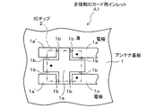
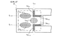
図1は本発明の実施の形態1の非接触ICカード用インレットA1の主要部分であるICチップ2とアンテナ基板1との接続の様子を示す平面図、図2はその断面図である。図1ではICチップ2が二点鎖線で図示されている。
(Embodiment 1)
FIG. 1 is a plan view showing a state of connection between an
本実施の形態の非接触ICカード用インレットA1は、アンテナ基板1におけるコイルアンテナ(図示せず)の電極1aに、ICチップ2の電極部にバンプ2aを形成し、接着剤3を用いてICチップ2をフェースダウンでアンテナ基板1に機械的に接合した構成となっている。アンテナ基板1の電極1aのパターンにおいて、電極間の溝1bの形状がICチップ2の存在領域内で非直線の状態に形成されている。図示の例では、90度に屈折する溝1bの形状となっている。1a′は電極1aと同じく電極パターンを形成する金属部分である。接着剤3としては、ACF(異方性導電フィルム)のみならず、NCP(非導電ペースト)、ACP(異方性導電性ペースト)も使用できる。
図3に基づいて本実施の形態による強度アップの作用について説明する。
In the non-contact IC card inlet A1 of this embodiment, bumps 2a are formed on the electrode portions of the
Based on FIG. 3, the effect | action of the intensity | strength increase by this Embodiment is demonstrated.
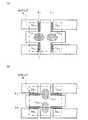
図3(a)は、縦方向の溝に沿った折り曲げ線での折り曲げに対する強度アップを説明するための模式図である。図3(a)に示すように、ある1つの縦方向の溝1b1の延長線L1を考える。この延長線L1上には別の溝1b2が存在しているが、これらの溝1b1,1b2はいずれもICチップ2の存在領域内で折れ曲がり、直線状の見通しができない状態とされている。すなわち、溝1b1あるいは溝1b2の延長線L1上に、ハッチングで示すように電極1aのパターンを形成する金属部分1c1が存在している。同様に溝1b3あるいは溝1b4の延長線L3上には、金属部分1c3が対応している。これらの金属部分1c1,1c3は、延長線L1,L3を折り曲げ線とするアンテナ基板1の折り曲げに対して抵抗要素として作用する。
FIG. 3A is a schematic diagram for explaining an increase in strength against folding along a folding line along a longitudinal groove. As shown in FIG. 3 (a), consider the extension line L 1 of the
図3(b)は、横方向の溝に沿った折り曲げ線での折り曲げに対する強度アップを説明するための模式図である。溝1b5,1b6の延長線L5上に対応する金属部分1c5が、延長線L5を折り曲げ線とするアンテナ基板1の折り曲げに対して抵抗要素となり、同様に、溝1b7,1b8の延長線L7上に対応する金属部分1c7が、延長線L7を折り曲げ線とするアンテナ基板1の折り曲げに対して抵抗要素となる。
FIG. 3B is a schematic diagram for explaining an increase in strength against bending along a bending line along a lateral groove. The metal portion 1c 5 corresponding to the extension line L 5 of the grooves 1b 5 and 1b 6 serves as a resistance element against the bending of the
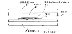
図4は、上記のように構成されたインレットA1を用いて作製された非接触ICカードの一例を示す。コア材4のくりぬき部にインレットA1を装填するとともに、コア材4の表面に表面保護シート6を、インレットA1のアンテナ基板1の表面に表面保護シート7をそれぞれラミネート加工する。
FIG. 4 shows an example of a non-contact IC card manufactured using the inlet A1 configured as described above. The inlet A1 is loaded into the hollow portion of the
非接触ICカードにおいて、ICチップ2の裏面(上方)から大きな力が加わったときに、アンテナ基板1が溝1bの部分で伸ばされることがない。すなわち、ICチップ2に応力がかからず、ICチップ2の破損が防止される。
In the non-contact IC card, when a large force is applied from the back surface (above) of the
なお、チップの形状や劈開(へきかい)面のために弱い方向が存在している場合には、アンテナ基板1の電極1aのパターンにおける溝1bの形状について、次のようにしてもよい。すなわち、ICチップ2の存在領域内で、直線状の見通しができない状態に折り曲げておくのを、前記の弱い方向の1方向に沿ってのみ実施するのでもよい。
In the case where a weak direction exists due to the shape of the chip and the cleavage plane, the shape of the
図5は、本発明の非接触ICカード用インレットを実現する電極パターンの別の例を示す。図6は、図5の場合の折り曲げに対する抵抗要素を示す模式図である。アンテナ基板1の電極1aのパターンにおいて、電極間の溝1bの形状がICチップ2の存在領域内で非直線の状態に形成されている。図示の例では、90度に屈折する溝1bの形状となっている。
FIG. 5 shows another example of an electrode pattern for realizing the contactless IC card inlet of the present invention. FIG. 6 is a schematic diagram showing a resistance element against bending in the case of FIG. In the pattern of the
図1、図3の場合は、中央の電極1aが十字形をしていて、縦方向の延長線L1上に2つの溝1b1,1b2が並び、また、縦方向の延長線L3上に2つの溝1b3,1b4が並び、また、横方向の延長線L5上に2つの溝1b5,1b6が並び、また、横方向の延長線L7上に2つの溝1b7,1b8が並んでいる。
In the case of FIGS. 1 and 3, the
これに対して、図5、図6の場合は、1つの電極1aが凸の字形をしていて、縦方向の延長線L9上に2つの溝1b9,1b10が並んでいるが、横方向の延長線L11上にあるのは1つの溝1b11のみであり、また、横方向の延長線L12上にあるのは1つの溝1b12のみである。このため、溝1b11,1b12の延長線L11,L12に対応する金属部分1c11,1c12は、それぞれの延長線を折り曲げ線とするアンテナ基板1の折り曲げに対し、図1の場合よりも、より大きな抵抗要素となる。
On the other hand, in the case of FIG. 5 and FIG. 6, one
図7は、本発明の非接触ICカード用インレットを実現する電極パターンのさらに別の例を示す。中央の電極1aは、十字形を変形した形状をしている。縦方向でも横方向でも、溝1bは同一直線上に2つ以上は存在しない形態としている。これにより、折り曲げに対する抵抗をさらに強化している。
FIG. 7 shows still another example of the electrode pattern for realizing the inlet for the non-contact IC card of the present invention. The
(実施の形態2)
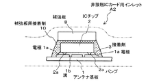
図8は本発明の実施の形態2の非接触ICカード用インレットA1の主要部分であるICチップ2とアンテナ基板1との接続状態を示す断面図である。図8において、実施の形態1の図2におけるのと同じ符号は同一構成要素を指しているので、詳しい説明は省略する。
(Embodiment 2)
FIG. 8 is a cross-sectional view showing a connection state between the
本実施の形態においては、実施の形態1の場合の図2に示す構造に加えて、ICチップ2の裏面に金属製の補強板8を補強板用接着剤10にて接着している。アンテナ基板1については、実施の形態1の場合と同様に、ICチップ2の存在領域内で直線状の見通しができないように溝1bを折り曲げる構造により、補強がなされている。このアンテナ基板1の補強と補強板8による補強とで、ICチップ2に対して実質的に両面補強を施している。これにより、特にICチップ2裏面からの点圧に対して強いインレットを実現できる。
In the present embodiment, in addition to the structure shown in FIG. 2 in the case of the first embodiment, a
図8に示すインレットA2を実施の形態1の場合と同様にコア材4および表面保護シート6,7を用いてラミネートして非接触ICカードを作製した場合には、両面補強板タイプと同じ効果が得られ、しかも、従来例の図14とは異なり、インレットの出っ張りは片面のみですむ。すなわち、強度の高い非接触ICカードを容易に作製することができる。
When the non-contact IC card is produced by laminating the inlet A2 shown in FIG. 8 using the
(実施の形態3)
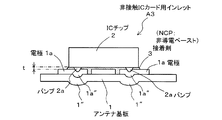
図9は本発明の実施の形態3の非接触ICカード用インレットの主要部分であるICチップ2とアンテナ基板1との接続状態を示す断面図である。図9において、実施の形態1の図2におけるのと同じ符号は同一構成要素を指しているので、詳しい説明は省略する。
(Embodiment 3)
FIG. 9 is a cross-sectional view showing a connection state between the
本実施の形態においては、実施の形態1の場合の図2に示す構造に対して、ICチップ2をアンテナ基板1に接合するための接着剤3として、NCP(非導電ペースト)を使用している。NCPは、ACF(異方性導電フィルム)やACP(異方性導電性ペースト)と違って、樹脂中に導電粒子が無い。そのため、ICチップ2のバンプ2aとアンテナ基板1の電極1aとの電気的接合を図るためには、ICチップ2をアンテナ基板1に押し付けて、バンプ2aを電極1aに喰い込ませている。1a″は喰い込みにより変形した電極1aの膨出部、1″は同じく喰い込みにより変形したアンテナ基板1の膨出部である。食い込みの結果として、電極1aとICチップ2との隙間寸法tが小さなものとなり、アンテナ基板1の補強の効果が増す。アンテナ基板1自体については、実施の形態1の場合と同様に、ICチップ2の存在領域内で直線状の見通しができないように溝1bを折り曲げる構造により、補強がなされている。以上の相乗により、さらに強度の高いインレットを実現できる。
In the present embodiment, NCP (non-conductive paste) is used as the adhesive 3 for bonding the
図9に示すインレットA3を実施の形態1の場合と同様にコア材4および表面保護シート6,7を用いてラミネートして非接触ICカードを作製した場合には、補強されたアンテナ基板3の電極1aが図14に示す従来例の補強板9の役割を果たし、カード表面(ICチップ裏面)からの落下衝撃に対して強い非接触ICカードを実現できる。
When the inlet A3 shown in FIG. 9 is laminated using the
なお、上記の実施の形態の説明では、直線状の見通しができない溝の折り曲げ形状につき、直角の折り曲げの場合のみを図示したが、その折り曲げの角度は、所要の効果を発揮する限りにおいて任意であり、鈍角でも鋭角でもよい。また、折り曲げは1回だけでなく、2回以上でもよい。また、単に屈折的な折り曲げに限る必要はなく、曲線的に折り曲げるのでもよい。 In the above description of the embodiment, only the case of a right-angle bend is shown for the groove bend shape in which a straight line cannot be seen, but the bend angle is arbitrary as long as the desired effect is exhibited. Yes, it may be obtuse or acute. Further, the bending may be performed not only once but also twice or more. Moreover, it is not necessary to be limited only to refractive bending, and it may be bent in a curved manner.
なお、上記説明では、補強板を片面のみ構成した場合を述べたが、さらに物理的強度が必要な場合は、同じ厚みで従来より強度の強い両面補強板構成にすることもできる。 In the above description, the case where the reinforcing plate is configured on only one side has been described. However, when further physical strength is required, a double-sided reinforcing plate configuration having the same thickness and higher strength than the conventional one can be used.
また、非接触ICカードの部分品のインレットとして説明したが、薄型のタグ、あるいは、ICカードと同等の機能をもつ商品にも適用できることはいうまでも無い。 Moreover, although it demonstrated as an inlet of the partial product of a non-contact IC card, it cannot be overemphasized that it can apply also to a thin tag or goods which have a function equivalent to an IC card.
本発明の非接触ICカード用インレットは、身分証明のためのIDカード、テレホンカードのようなプリペイドカード、キャシュカード、定期券等に有用である。 The inlet for contactless IC card of the present invention is useful for ID cards for identification, prepaid cards such as telephone cards, cash cards, commuter passes, and the like.
A1〜A5 インレット
1 アンテナ基板
1a 電極
1a′ 金属部分
1b 溝
2 ICチップ
2a バンプ
3 接着剤
4,5 コア材
6,7 表面保護用シート
8,9 補強板
10 補強板用接着剤
A1 to
Claims (4)
前記アンテナ基板の前記電極に対してフェースダウンで電気的に接合されたICチップとを備え、
前記アンテナ基板の前記電極のパターンは、電極間の溝の形状が前記ICチップの存在領域内で少なくとも一方向に沿っては直線的見通し不可の折り曲げ状態に形成されていることを特徴とする非接触ICカード用インレット。 An antenna substrate having a coil antenna and an electrode;
An IC chip electrically connected face down to the electrodes of the antenna substrate,
The electrode pattern of the antenna substrate is formed in a bent state in which the shape of the groove between the electrodes is not linearly visible along at least one direction in the region where the IC chip exists. Inlet for contact IC card.
Priority Applications (1)
| Application Number | Priority Date | Filing Date | Title |
|---|---|---|---|
| JP2004110930A JP2005293460A (en) | 2004-04-05 | 2004-04-05 | Non-contact IC card inlet and non-contact IC card |
Applications Claiming Priority (1)
| Application Number | Priority Date | Filing Date | Title |
|---|---|---|---|
| JP2004110930A JP2005293460A (en) | 2004-04-05 | 2004-04-05 | Non-contact IC card inlet and non-contact IC card |
Publications (1)
| Publication Number | Publication Date |
|---|---|
| JP2005293460A true JP2005293460A (en) | 2005-10-20 |
Family
ID=35326289
Family Applications (1)
| Application Number | Title | Priority Date | Filing Date |
|---|---|---|---|
| JP2004110930A Pending JP2005293460A (en) | 2004-04-05 | 2004-04-05 | Non-contact IC card inlet and non-contact IC card |
Country Status (1)
| Country | Link |
|---|---|
| JP (1) | JP2005293460A (en) |
Cited By (2)
| Publication number | Priority date | Publication date | Assignee | Title |
|---|---|---|---|---|
| JP2007148672A (en) * | 2005-11-25 | 2007-06-14 | Matsushita Electric Ind Co Ltd | IC module and non-contact IC card |
| JP2012053831A (en) * | 2010-09-03 | 2012-03-15 | Murata Mfg Co Ltd | Mounting structure of rfic chip |
Citations (8)
| Publication number | Priority date | Publication date | Assignee | Title |
|---|---|---|---|---|
| JPS62185072U (en) * | 1986-05-15 | 1987-11-25 | ||
| JPS63148466U (en) * | 1987-03-20 | 1988-09-29 | ||
| JPS63194773U (en) * | 1987-06-04 | 1988-12-15 | ||
| JPH01115583U (en) * | 1988-01-29 | 1989-08-03 | ||
| JPH07263587A (en) * | 1994-03-22 | 1995-10-13 | Toshiba Corp | Semiconductor package |
| JP2001143036A (en) * | 1999-11-17 | 2001-05-25 | Dainippon Printing Co Ltd | Non-contact data carrier, IC chip used for the same, and method of attaching IC chip to non-contact data carrier |
| JP2001237260A (en) * | 2000-02-22 | 2001-08-31 | Hitachi Ltd | Semiconductor device |
| JP2002141369A (en) * | 2000-11-02 | 2002-05-17 | Omron Corp | Semiconductor device and data carrier device |
-
2004
- 2004-04-05 JP JP2004110930A patent/JP2005293460A/en active Pending
Patent Citations (8)
| Publication number | Priority date | Publication date | Assignee | Title |
|---|---|---|---|---|
| JPS62185072U (en) * | 1986-05-15 | 1987-11-25 | ||
| JPS63148466U (en) * | 1987-03-20 | 1988-09-29 | ||
| JPS63194773U (en) * | 1987-06-04 | 1988-12-15 | ||
| JPH01115583U (en) * | 1988-01-29 | 1989-08-03 | ||
| JPH07263587A (en) * | 1994-03-22 | 1995-10-13 | Toshiba Corp | Semiconductor package |
| JP2001143036A (en) * | 1999-11-17 | 2001-05-25 | Dainippon Printing Co Ltd | Non-contact data carrier, IC chip used for the same, and method of attaching IC chip to non-contact data carrier |
| JP2001237260A (en) * | 2000-02-22 | 2001-08-31 | Hitachi Ltd | Semiconductor device |
| JP2002141369A (en) * | 2000-11-02 | 2002-05-17 | Omron Corp | Semiconductor device and data carrier device |
Cited By (3)
| Publication number | Priority date | Publication date | Assignee | Title |
|---|---|---|---|---|
| JP2007148672A (en) * | 2005-11-25 | 2007-06-14 | Matsushita Electric Ind Co Ltd | IC module and non-contact IC card |
| JP2012053831A (en) * | 2010-09-03 | 2012-03-15 | Murata Mfg Co Ltd | Mounting structure of rfic chip |
| US8546927B2 (en) | 2010-09-03 | 2013-10-01 | Murata Manufacturing Co., Ltd. | RFIC chip mounting structure |
Similar Documents
| Publication | Publication Date | Title |
|---|---|---|
| JP4108779B2 (en) | Circuit chip mounted card and circuit chip module | |
| CN104680227B (en) | Chip card module arrangement, chip card and method for producing the same | |
| US7746234B2 (en) | RFID tag | |
| US7857202B2 (en) | Method and apparatus for a contactless smartcard incorporating a pressure sensitive switch | |
| WO2007034764A1 (en) | Noncontact information storage medium and method for manufacturing same | |
| KR100760504B1 (en) | Radio frequency identification tag | |
| CN104021413A (en) | Chip arrangement and a method for manufacturing a chip arrangement | |
| JP2001043342A (en) | Chip card | |
| JP2005293460A (en) | Non-contact IC card inlet and non-contact IC card | |
| US20050179122A1 (en) | IC card | |
| KR100802786B1 (en) | IC card manufacturing method | |
| JP4813160B2 (en) | IC module and non-contact IC card | |
| JP2004264983A (en) | Non-contact IC card | |
| JP4754344B2 (en) | RFID tag | |
| JP6451298B2 (en) | Dual interface IC card and IC module used for the IC card | |
| JP3902969B2 (en) | RF-ID media | |
| JP2006127254A (en) | Portable electronic device | |
| JP2006074044A (en) | Chip module | |
| JPH11134458A (en) | Ic card | |
| JP4845179B2 (en) | IC chip reinforcing plate and paper | |
| KR20230119921A (en) | Inlay sheet and credit card having the same | |
| JP2006195618A (en) | IC module and IC card using the same | |
| CN210348510U (en) | Fingerprint identification module and electronic product | |
| JP2000242761A (en) | Card type electronic circuit board | |
| JP2004118502A (en) | Combination IC card |
Legal Events
| Date | Code | Title | Description |
|---|---|---|---|
| A621 | Written request for application examination |
Free format text: JAPANESE INTERMEDIATE CODE: A621 Effective date: 20070207 |
|
| A131 | Notification of reasons for refusal |
Free format text: JAPANESE INTERMEDIATE CODE: A131 Effective date: 20100209 |
|
| A02 | Decision of refusal |
Free format text: JAPANESE INTERMEDIATE CODE: A02 Effective date: 20100601 |