JP2005293205A - Storage control device, control method, and control program. - Google Patents
Storage control device, control method, and control program. Download PDFInfo
- Publication number
- JP2005293205A JP2005293205A JP2004107030A JP2004107030A JP2005293205A JP 2005293205 A JP2005293205 A JP 2005293205A JP 2004107030 A JP2004107030 A JP 2004107030A JP 2004107030 A JP2004107030 A JP 2004107030A JP 2005293205 A JP2005293205 A JP 2005293205A
- Authority
- JP
- Japan
- Prior art keywords
- write
- storage
- data
- cache memory
- raid
- Prior art date
- Legal status (The legal status is an assumption and is not a legal conclusion. Google has not performed a legal analysis and makes no representation as to the accuracy of the status listed.)
- Granted
Links
Images


Classifications
-
- G—PHYSICS
- G06—COMPUTING OR CALCULATING; COUNTING
- G06F—ELECTRIC DIGITAL DATA PROCESSING
- G06F12/00—Accessing, addressing or allocating within memory systems or architectures
- G06F12/02—Addressing or allocation; Relocation
- G06F12/08—Addressing or allocation; Relocation in hierarchically structured memory systems, e.g. virtual memory systems
- G06F12/0802—Addressing of a memory level in which the access to the desired data or data block requires associative addressing means, e.g. caches
- G06F12/0804—Addressing of a memory level in which the access to the desired data or data block requires associative addressing means, e.g. caches with main memory updating
-
- G—PHYSICS
- G06—COMPUTING OR CALCULATING; COUNTING
- G06F—ELECTRIC DIGITAL DATA PROCESSING
- G06F12/00—Accessing, addressing or allocating within memory systems or architectures
- G06F12/02—Addressing or allocation; Relocation
- G06F12/08—Addressing or allocation; Relocation in hierarchically structured memory systems, e.g. virtual memory systems
- G06F12/0802—Addressing of a memory level in which the access to the desired data or data block requires associative addressing means, e.g. caches
- G06F12/0866—Addressing of a memory level in which the access to the desired data or data block requires associative addressing means, e.g. caches for peripheral storage systems, e.g. disk cache
Landscapes
- Engineering & Computer Science (AREA)
- Theoretical Computer Science (AREA)
- Physics & Mathematics (AREA)
- General Engineering & Computer Science (AREA)
- General Physics & Mathematics (AREA)
- Memory System Of A Hierarchy Structure (AREA)
Abstract
【課題】 レベルの異なる複数のRAID装置へのデータのライトバックを、一部のRAID装置に偏ることなく実行する。
【解決手段】 RAID制御装置1内のキャッシュメモリ2に格納されているデータの複数のRAID装置3へのライトバックをLRU法によって行う手段4と、手段4によって実行されているライトバックの数が少ない装置3を選択して、選択した装置3に対してデータのライトバックを行う手段5とを備える。
【選択図】図1PROBLEM TO BE SOLVED: To perform data write-back to a plurality of RAID devices having different levels without biasing to some RAID devices.
SOLUTION: Means 4 for performing write back of data stored in a cache memory 2 in a RAID control device 1 to a plurality of RAID devices 3 by the LRU method, and the number of write backs executed by the means 4 are as follows. Means 5 for selecting a small number of devices 3 and writing data back to the selected devices 3.
[Selection] Figure 1
Description
本発明はデータ記憶方式に係り、さらに詳しくはディスクアレイを用いた磁気ディスクシステムに対応して、ホストコンピュータからの指示によってデータのリード/ライトが行われるキャッシュメモリを備えた磁気ディスク制御装置に関する。 The present invention relates to a data storage system, and more particularly, to a magnetic disk control apparatus having a cache memory in which data is read / written in response to an instruction from a host computer, corresponding to a magnetic disk system using a disk array.
近年、データ記録の不揮発性、大容量性などの特徴を持つ磁気ディスク装置、光ディスク装置などのディスク装置がコンピュータの外部記憶装置として広く用いられている。このような磁気ディスク装置等においてデータの内容を二重化したり、パリティデータなどの冗長な情報を付け加えて記録したりするためのディスク装置としてRAID(リダンダント・アレイ・オブ・インエクスペンシブ・ディスク)装置が用いられている。 In recent years, disk devices such as magnetic disk devices and optical disk devices having characteristics such as non-volatility and large capacity of data recording have been widely used as external storage devices for computers. A RAID (Redundant Array of Inexpensive Disk) device is used as a disk device for duplicating data contents in such a magnetic disk device or the like and adding redundant information such as parity data. It is used.
このようなRAID装置と、例えばホストコンピュータとの間でのデータの転送を制御するRAID制御装置は大容量のキャッシュメモリを搭載し、そのキャッシュメモリに一時データを保持することによってデータ転送の性能向上を図っている。またこのような制御装置の配下には、扱うべきデータ量の増大に伴って膨大な数の多種多量なRAID装置、すなわちRAID0からRAID5までのレベルのRAID装置が多数接続されて使用される。
A RAID control device that controls data transfer between such a RAID device and, for example, a host computer has a large-capacity cache memory and improves data transfer performance by holding temporary data in the cache memory. I am trying. Under such control devices, a large number of various RAID devices, that is, RAID devices at levels from
図14はこのようなRAID制御装置におけるキャッシュデータ管理方式の従来例の説明図である。同図においてRAID制御装置のキャッシュメモリ内のデータは、ホストコンピュータによる使用頻度の最も高いMRUの位置のデータから、最も使用頻度の低いLRUの位置のデータまで、例えばリンクを用いて並べられ、ホストコンピュータからのアクセスがあった場合にはキャッシュヒットしたものとして、最も使用頻度の高いデータとしてMRUの位置に接続される。 FIG. 14 is an explanatory diagram of a conventional example of a cache data management method in such a RAID control apparatus. In the figure, the data in the cache memory of the RAID controller is arranged using, for example, a link from the data at the MRU position where the host computer is used most frequently to the data at the LRU position where the frequency is least used. When there is an access from the computer, it is connected to the location of the MRU as the most frequently used data as a cache hit.
図14においてホストコンピュータからキャッシュメモリに書き込まれたデータに対してはライトバック、すなわち非同期でのディスク装置への書き出しが行われる。このRAID装置(ディスク)へのデータのライトバックは、データ記憶システムとしての全体的な性能を考慮して、LRU法によってアクセス頻度の低いデータ、すなわちLRUの位置のデータから実行される。 In FIG. 14, the data written from the host computer to the cache memory is written back, that is, written asynchronously to the disk device. The write back of data to the RAID device (disk) is executed from data with low access frequency, that is, data at the location of the LRU by the LRU method in consideration of the overall performance as a data storage system.
しかしキャッシュメモリからRAID装置(ディスク)への書き出し性能は、RAIDタイプ(レベル)によって異なる。すなわちデータを複数のディスク装置に分散して書き込むRAID0+1、RAID5では複数のディスクが並列に動作するためにスループット性能が高く、逆に2台のディスク装置にそれぞれ同じ内容のデータを書き込むRAID1ではディスクの性能以上の能力が出せないため、スループット性能が低くなることになる。
However, the writing performance from the cache memory to the RAID device (disk) differs depending on the RAID type (level). That is, in
このようにライトバック性能が異なる複数のRAID装置に書き込むべきデータを1つのキャッシュメモリを介するデータ転送という形式で管理する場合、ライトバック性能が悪いRAID1の装置へのライトデータがキャッシュメモリ上で滞留しやすくなる。キャッシュメモリがそのような滞留データで埋め尽くされてしまうと、それ以降はRAID1のディスク装置へのライトバック性能に引きずられ、スループット性能が良いRAID0+1、RAID5に対するアクセスにおいても性能低下が起こるという問題点があった。
When data to be written to a plurality of RAID devices having different write-back performances is managed in the form of data transfer via one cache memory, write data to a
このようなRAIDデータ記憶システムに関する従来技術として次のような文献がある。
特許文献1では、ディスクキャッシュ機能の最適化を図るために、例えばRAID5の動作でもディスクリードを必要とせずにパリティを計算できるRAID3的なアクセスを可能とするように、キャッシュブロック上に有効データを準備しておくディスクキャッシュ装置が開示されている。
In
特許文献2には、ライトバックキャッシュ方式のストレージ装置において、ホスト装置から指定される書込み対象のアドレスが連続していない場合でも、シーケンシャルなデータの書き出しをもれなく実行することができるライトキャッシュ制御方法を用いてスループットを改善する技術が開示されている。
しかしながらこのような従来技術においても、RAID装置として各種のレベルの装置が混在する場合に、ライトバック性能が悪いRAID装置の性能に引きずられてデータ記憶システムとしての全体的性能が低下するという問題点を解決することができない。 However, even in such a conventional technique, when various levels of devices are mixed as RAID devices, the overall performance as a data storage system is deteriorated due to being dragged by the performance of a RAID device having poor write back performance. Can not be solved.
本発明の課題は、上述の問題点に鑑み、レベルが異なる複数のRAID装置がRAID制御装置の配下に存在する場合にも、できるだけ多くのRAID装置へのライトバックをスケジュール可能とすることによって、データ記憶システムとしての全体的な性能を向上させることである。 In view of the above-described problems, the problem of the present invention is that it is possible to schedule write-back to as many RAID devices as possible even when a plurality of RAID devices having different levels exist under the control of a RAID control device. It is to improve the overall performance of the data storage system.
図1は本発明の記憶制御装置、例えばRAID制御装置の原理構成ブロック図である。同図において記憶制御装置1はキャッシュメモリ2を備え、複数の記憶装置3、例えばRAID装置を制御するものであり、基本的構成要素としてLRUライトバック手段4とライトバックスケジュール処理手段5とを少なくとも備える。
FIG. 1 is a block diagram showing the principle configuration of a storage control device of the present invention, for example, a RAID control device. In the figure, the
LRUライトバック手段4は、記憶制御装置1の内部のキャッシュメモリ2に格納されているデータの複数の記憶装置3側へのライトバックを、LRU法(アルゴリズム)によって行うものであり、ライトバックスケジュール処理手段5はLRUライトバック手段4によって実行されているライトバックの数が少ない記憶装置3を選択して、選択した記憶装置3に対するデータのライトバックを行うものである。
The LRU write-back means 4 performs write-back of data stored in the
発明の実施の形態においては記憶制御装置1が、複数の記憶装置3をその記憶装置3が実行しているライトバックの数によって複数のグループに分割した結果を記憶するライトバックグループ管理手段、例えばライトバックグループ管理テーブルをさらに備え、ライトバックスケジュール処理手段5がライトバックグループ管理手段の記憶内容に従ってライトバックの数が少ないグループ内の記憶装置3を選択することもできる。
In the embodiment of the invention, the
また実施の形態においては、複数の記憶装置3毎に実行されているライトバックの数を記憶する記憶装置管理手段、例えばRAID装置毎の管理テーブルをさらに備え、ライトバックスケジュール処理手段5が記憶装置管理手段の記憶内容にしたがってライトバックの数が少ない記憶装置3を選択することもできる。
In the embodiment, the storage device management means for storing the number of write-backs executed for each of the plurality of
さらに実施の形態においては、記憶制御装置内のキャッシュメモリの容量を分割して、複数の記憶装置3に割当てるキャッシュメモリ割当手段と、割当てられた容量の内でキャッシュメモリにデータが格納されていない未使用領域の容量を記憶装置毎に記憶する記憶装置管理手段、例えばRAID装置毎の管理テーブルとをさらに備え、ライトバックスケジュール処理手段5が記憶装置管理手段の記憶内容にしたがって未使用領域の少ない記憶装置3を選択することもできる。
Further, in the embodiment, the cache memory allocation unit that divides the capacity of the cache memory in the storage control device and allocates the cache memory to the plurality of
この場合、記憶装置3に割当てられたキャッシュメモリの容量の内部に格納されているデータのキューを記憶装置3毎に管理するキャッシュメモリ管理手段、例えばキャッシュメモリ管理テーブルをさらに備え、ライトバックスケジュール処理手段5が選択した記憶装置3に対応するキューにおけるLRUの位置のデータのライトバックを行うこともできる。
In this case, a cache memory management means for managing, for each
また発明の実施の形態においては、前述の記憶装置3が複数のディスクを備えるRAID装置であり、記憶制御装置1が複数のRAID装置を制御するRAID制御装置であることもできる。
In the embodiment of the invention, the
次に本発明のデータ記憶システムは、自装置内のキャッシュメモリに格納されているデータの複数の記憶装置側へのライトバックLRU法によって行うLRUライトバック手段と、LRUライトバック手段によって実行されているライトバックの数が少ない記憶装置を選択し、選択した記憶装置に対するデータのライトバックを行うライトバックスケジュール処理手段とを備える記憶制御装置と、その記憶制御装置によって制御される複数の記憶装置とによって構成される。 Next, the data storage system of the present invention is executed by the LRU write-back means for performing the write-back LRU method for the data stored in the cache memory in the self-device, and the LRU write-back means. A storage control device that includes a write-back schedule processing unit that selects a storage device that has a small number of write-backs and performs data write-back to the selected storage device, and a plurality of storage devices that are controlled by the storage control device; Consists of.
本発明の記憶制御方法におていは、記憶制御装置内のキャッシュメモリに格納されているデータの複数の記憶装置側へのライトバックをLRU法によって実行し、LRU法によって実行されているライトバックの数が少ない記憶装置を選択して、選択した記憶装置に対するデータのライトバックを実行する方法が用いられる。 In the storage control method of the present invention, write back to a plurality of storage devices of data stored in the cache memory in the storage control device is executed by the LRU method, and the write back executed by the LRU method is performed. A method is used in which a storage device having a small number of data is selected and data is written back to the selected storage device.
またこの方法を計算機によって実行するためのプログラム、およびそのプログラムを格納した計算機読出し可能可搬型記憶媒体が用いられる。
以上のように本発明によれば、まず記憶制御装置、たとえばRAID制御装置内のキャッシュメモリを複数の記憶装置、例えばRAID装置に対応して分割して割当てることによって、キャッシュメモリの内部がスループット性能の悪い記憶装置に掃き出すべきデータで埋め尽くされることが防止される。
In addition, a program for executing this method by a computer and a computer-readable portable storage medium storing the program are used.
As described above, according to the present invention, first, a cache memory in a storage control device, for example, a RAID control device is divided and allocated corresponding to a plurality of storage devices, for example, RAID devices. It is prevented that the storage device with bad data is filled with data to be swept out.
またこのRAID装置毎に割当てられたキャッシュメモリ容量の内で未使用のメモリ容量を管理し、未使用領域が少ないRAID装置に対するライトバックを実行することによって、キャッシュメモリの空き容量を確保することができる。 Further, it is possible to secure an unused capacity of the cache memory by managing an unused memory capacity in the cache memory capacity allocated to each RAID apparatus and executing a write back to the RAID apparatus having a small unused area. it can.
さらにRAID装置毎にライトバックの実行数を管理するとともに、ライトバックの実行数によってRAID装置をグループ化することによって、ライトバック実行数の少ないRAID装置の検索が容易となり、多くのRAID装置に対してライトバックをスケジュールすることが可能となる。 Furthermore, by managing the number of write-back executions for each RAID device and grouping RAID devices according to the number of write-back executions, it is easy to search for RAID devices with a small number of write-back executions, and for many RAID devices. And write back can be scheduled.
本発明によれば、RAID制御装置の配下にRAIDタイプ(レベル)の異なる複数のRAID装置が存在する場合にも、ライトバック性能が悪いRAID装置による性能低下を防止し、データ記憶システムとしての全体性能を向上させることが可能となり、RAID記憶装置システムにおける性能向上に寄与するところが大きい。 According to the present invention, even when there are a plurality of RAID devices having different RAID types (levels) under the RAID control device, the performance deterioration due to the RAID device having poor write back performance is prevented, and the entire data storage system is provided. The performance can be improved, and it greatly contributes to the performance improvement in the RAID storage system.
図2は本発明のRAID制御装置が用いられるデータ記憶システム全体構成ブロック図である。同図においてシステムはRAID制御装置10、ホストコンピュータ(サーバ)11、および複数のRAID装置12によって構成されている。
FIG. 2 is a block diagram of the entire configuration of the data storage system in which the RAID control apparatus of the present invention is used. In FIG. 1, the system includes a RAID control device 10, a host computer (server) 11, and a plurality of
RAID制御装置10は、ホストコンピュータ11側との間のデータ転送を制御するためのチャネルアダプタ13、RAID装置12との間でデータ転送を制御するデバイスアダプタ14、およびRAID制御装置10の全体を制御する中央制御部15を備えている。
The RAID control apparatus 10 controls the
中央制御部15は、ホストコンピュータ11とRAID装置12との間で転送が行われるデータを一時的に保持するキャッシュメモリ16、各種の制御情報を格納するテーブルとしてのキャッシュメモリ管理テーブル17、RAID装置毎の管理テーブル18、およびライトバックグループ管理テーブル19を備えている。ここでキャッシュメモリ16は、例えば2GBの搭載容量を持つものとする。
The
図2においてRAID装置12は、RLU(レイド・ロジカル・ユニット)#00からRLU#05までの6台があるものとし、このうちRLU#04、およびRLU#05のレベルはRAID1である。RLU#00とRLU#01とのレベルはRAID5であり、RLU#00はデータ格納用のディスク4台とバリティ格納用の1台のディスクを備え、RLU#01はデータ格納用の15台、バリティ格納用の1台のディスクを備えるものとする。RLU#02、およびRLU#03のレベルはRAID0+1であり、RLU#02はデータ格納用の4台、ミラー用の4台のディスクを備え、RLU#03はデータ格納用の8台とミラー用の8台のディスクを備えるものとする。
In FIG. 2, it is assumed that there are six
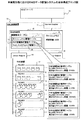
本実施形態においては、まずRAID制御装置10の内部のキャッシュメモリ16をRAID装置12のスループット性能に対応して分割し、分割結果を各RAID装置12に割り付けることによって、キャッシュメモリ16がスループット性能の悪いRAID装置にライトバックすべきデータで埋め尽くされることを防止するものとする。図3はこのキャッシュメモリ分割割付処理のフローチャートである。同図において装置の電源がオンされ、装置立上げ処理の開始に伴ってキャッシュメモリ分割処理が初期化処理の1つとして実行される。
In this embodiment, first, the
図3のステップS1においてRAID制御装置10のキャッシュメモリ容量、ここでは2GBが獲得され、それがキャッシュメモリ管理テーブル17に設定され、ステップS2でRAID制御装置10内の構成情報が読み込まれ、ステップS3でその構成情報からRAID制御装置10の配下の複数のRAID装置12に関する情報が獲得される。そしてその情報に対応して複数のRAID装置12に対してそれぞれステップS4からステップS9の処理が実行される。
In step S1 of FIG. 3, the cache memory capacity of the RAID controller 10, here 2 GB, is acquired and set in the cache memory management table 17, the configuration information in the RAID controller 10 is read in step S2, and step S3 Thus, information on the plurality of
まずステップS4で処理を行うべきRAID装置12に関する情報が存在するか否かが判定され、存在する場合にはステップS5でRAIDタイプ(レベル)とディスクの数が獲得され、ステップS6でRAIDのタイプがRAID5であるか否かが判定され、5である場合にはステップS7で割当てるべきキャッシュ容量が64MB×ディスク数として計算され、RAID5でない場合には、ステップS8で128MB×ディスク数としてキャッシュ容量が計算された後に、ステップS9でそのRAID装置毎の管理テーブル18に求められたキャッシュ容量が設定されて、ステップS4以降の処理が繰り返される。全てのRAID装置12に対する処理が終了した時点でキャッシュメモリ分割処理を終了する。
First, in step S4, it is determined whether or not there is information on the
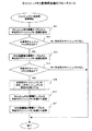
図4はキャッシュメモリ使用時処理のフローチャートである。同図は、例えば図2のRAID制御装置10の内部のキャッシュメモリ16に、ホストコンピュータ11側からデータが格納される場合の制御情報(テーブル)を利用した処理のフローチャートである。
FIG. 4 is a flowchart of processing when the cache memory is used. This figure is a flowchart of processing using control information (table) when data is stored from the
図4において処理が開始されると、まずステップS11で図2のキャッシュメモリ管理テーブル17からキャッシュメモリ16内の未使用のキャッシュメモリ容量が獲得され、ステップS12で未使用のキャッシュメモリ、すなわちデータを格納できるキャッシュメモリの容量があるか否かが判定され、ない場合には直ちに処理を終了する。
When processing is started in FIG. 4, first, in step S11, an unused cache memory capacity in the
未使用のキャッシュメモリがある場合には、ステップS13でRAID装置毎の管理テーブル18から未使用のキャッシュメモリ容量が獲得される。この処理では、図3においてそれぞれのRAID装置12に対して設定されたキャッシュ容量、例えばアドレスによって指定されるキャッシュ容量に対応して、データを格納すべきアドレスに対応するRAID装置毎の管理テーブル18から未使用のキャッシュメモリ容量が獲得されるが、次のステップS14でそのアドレスに対応するRAID装置毎の管理テーブル18において未使用のキャッシュメモリがあるか否かが判定され、未使用のキャッシュメモリがない、すなわちそのアドレスにデータが格納できない場合にも直ちに処理を終了する。
If there is an unused cache memory, an unused cache memory capacity is acquired from the management table 18 for each RAID device in step S13. In this process, the management table 18 for each RAID device corresponding to the address where the data is to be stored corresponds to the cache capacity set for each
ステップS14で未使用のキャッシュメモリがある場合には、ステップS15でその未使用のキャッシュメモリに、例えばデータが格納されるとともにそのキャッシュメモリを使用中状態とする処理が行われ、ステップS16でキャッシュメモリ管理テーブル17の未使用キャッシュメモリ容量から使用中状態とされた容量が減算され、ステップS17でRAID装置毎の管理テーブル18に格納されている未使用キャッシュメモリ容量、すなわちそのRAID装置12に割当てられたキャッシュメモリ容量の中で使用されていないキャッシュメモリ容量から使用中状態とされた容量が減算されて処理を終了する。なおRAID装置毎の管理テーブルの具体的な内容についてはさらに図6で後述する。
If there is an unused cache memory in step S14, for example, data is stored in the unused cache memory in step S15, and processing for setting the cache memory in use is performed. The used capacity is subtracted from the unused cache memory capacity of the memory management table 17 and assigned to the unused cache memory capacity stored in the management table 18 for each RAID device in step S17, that is, to the
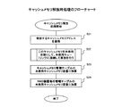
図5はキャッシュメモリ解放時のフローチャートである。この処理は、例えばキャッシュメモリからデータが削除される場合に実行される処理であり、まずステップS21で解放されるキャッシュメモリのアドレスが獲得され、ステップS22でこのキャッシュメモリが未使用状態とされ、例えばキャッシュメモリ管理テーブル17に格納されている未使用キュー(リンク)にそのアドレスのキャッシュメモリが接続されて解放が行われ、ステップS23でキャッシュメモリ管理テーブル17の未使用キャッシュメモリ容量に解放された容量が加算され、ステップS24でRAID装置毎の管理テーブル18内の同じく未使用キャッシュメモリ容量に解放された容量が加算されて処理を終了する。 FIG. 5 is a flowchart when the cache memory is released. This process is executed when data is deleted from the cache memory, for example. First, the address of the cache memory to be released is acquired in step S21, and the cache memory is set to an unused state in step S22. For example, the cache memory at that address is connected to an unused queue (link) stored in the cache memory management table 17 and released, and the cache memory management table 17 is released to the unused cache memory capacity in step S23. The capacity is added, and the released capacity is added to the unused cache memory capacity in the management table 18 for each RAID device in step S24, and the process ends.
図6は図2のRAID装置毎の管理テーブル18とライトバックグループ管理テーブル19の格納内容の具体例の説明図である。RAID装置毎の管理テーブル18は、RLU(RAID ロジカル・ユニット)管理テーブルとも呼ばれ、各RAID装置12、ここではRLU#00からRLU#4095までの全部で4096台のRAID装置12に割当てられたキャッシュメモリのページ数、割当てられたページの中で未使用のページ数としてのページレフト、およびライトバックの実行数がそれぞれのRAID装置12に対して格納されている。
FIG. 6 is an explanatory diagram of a specific example of the contents stored in the management table 18 and the write-back group management table 19 for each RAID device in FIG. The management table 18 for each RAID device is also called an RLU (RAID Logical Unit) management table, and is assigned to each
ライトバックグループ管理テーブル19は、ライトバックの実行数が同じくらいのRAID装置をグループ化して管理するものであり、ここではグループAはキャッシュメモリが未使用でライトバックが不必要なRAID装置群、グループBはキャッシュメモリが使用され、ライトバックの実行数が0のRAID装置群、グループCはキャッシュメモリが使用され、ライトバックの実行数が1から5までのRAID装置群、グループDはキャッシュメモリが使用され、ライトバックの実行数が6以上のRAID装置群であり、図6では各グループからリンクによって接続される形式でRAID装置毎の管理テーブル18が管理される。ここではグループB、すなわちRLU#02とRLU#4095においてライトバックの実行数が少なく、また未使用ページ容量が少ないことからライトバックが必要であることが容易に判定される。
The write-back group management table 19 manages RAID devices having the same number of write-backs as a group. Here, the group A is a RAID device group in which cache memory is unused and write-back is unnecessary. Group B uses a cache memory and a RAID device group in which the number of write-back executions is 0. Group C uses a cache memory, and a RAID device group in which the number of write-back executions is 1 to 5, and group D is a cache memory. Are used, and the number of write-back executions is six or more. In FIG. 6, the management table 18 for each RAID device is managed in a form connected from each group by a link. Here, in group B, that is,
図7は本実施形態におけるライトバック実行処理のフローチャートである。本実施形態では、前述のようにまず通常のLRU法によるライトバックスケジュールによってライトバックの実行処理が行われた後に、ライトバックの実行数の少ないRAID装置がチェックされ、RAID装置単位にさらにライトバックスケジュールが実行されるが、図7のライトバック実行処理は、通常のLRU法によるライトバックにおいても、またRAID装置単位のライトバックにおいても同様に用いられるものである。 FIG. 7 is a flowchart of the write-back execution process in this embodiment. In the present embodiment, as described above, after the write back execution process is first performed according to the write back schedule according to the normal LRU method, RAID devices with a small number of write back executions are checked, and further write back is performed for each RAID device. Although the schedule is executed, the write-back execution process of FIG. 7 is used in the same way for the write-back by the normal LRU method and the write-back for each RAID device.
図7において処理が開始されると、まずステップS31でライトバック対象のキャッシュデータが獲得され、ステップS32で図2のデバイスアダプタ14に対してライトバックデータのキャッシュアドレスが通知され、ステップS33でそのデータのライトバックが指示される。そしてステップS34でライトバックすべきキャッシュデータに対応するRLUの番号からRAID装置毎の管理テーブル18が求められ、ステップS35でそのテーブルのライトバック実行数に1が加算され、ステップS36で加算された実行数に対応してライトバックグループ管理テーブル19におけるグループが求められる。
When the process is started in FIG. 7, first, the write-back target cache data is acquired in step S31, the write-back data cache address is notified to the
続いてステップS37でライトバック実行数に1を加算した結果、RAID装置12が現在のグループと同一グループに留まっているか否かが判定され、同一グループである場合には直ちに処理を終了し、グループの変更を行うべき場合には、ステップS38で現在のグループからそのRAID装置毎の管理テーブル18が切断され、ステップS39でその管理テーブル18が新しいグループに接続されて処理を終了する。
Subsequently, in step S37, as a result of adding 1 to the number of write back executions, it is determined whether or not the
図8は、図2のデバイスアダプタ14からライトバックの実行処理が完了したことを示す通知を受信した後に行われるライトバック完了処理のフローチャートである。実際にはキャッシュメモリ16からRAID装置12へのデータのライトバックにはかなりの時間を要するため、図7においてデバイスアダプタ14にデータのライトバックが指示されてから、図8のライトバック完了処理が開始されるまでには、かなりの時間が必要となる。
FIG. 8 is a flowchart of the write-back completion process performed after receiving a notification indicating that the write-back execution process has been completed from the
図8のステップS41でライトバック対象のキャッシュデータが獲得され、ステップS42でそのライトバックデータがRAID装置毎のキャッシュデータのキューから切断される。このRAID装置毎のキャッシュデータのキューは図9に示される。 In step S41 of FIG. 8, cache data to be written back is acquired, and in step S42, the write back data is disconnected from the cache data queue for each RAID device. The cache data queue for each RAID device is shown in FIG.
図9においてMRUの位置、すなわち最も使用頻度の高いデータからLRUの位置、すなわち最も使用頻度の低いデータまでのそれぞれのデータに対してRAID装置毎のキュー(リンク)が張られている。同図において実線の矢印は、RAID1のRAID装置のデータのリンク、一点鎖線は、RAID5の装置のデータのリンク、点線はRAID0+1の装置のデータのリンク(それぞれ双方向)を示し、上向きの矢印は、キューの先頭側のキャッシュデータを示し、その矢印をプリビアスポインタと呼び、下の矢印は末尾側のキャッシュデータを示し、その矢印をネクストポインタと呼ぶことにする。なお、図2では各タイプのRAID装置が2台ずつ存在するため、それぞれの装置に対応して、例えば実線のキュー(リンク)は2本張られることになる。
In FIG. 9, a queue (link) for each RAID device is established for each data from the MRU position, that is, the most frequently used data to the LRU position, that is, the least frequently used data. In the figure, solid line arrows indicate
図8のステップS42でライトバックデータがキューから切断された後に、ステップS43でライトバックが行われたキャッシュデータに対応するRLU番号からRAID装置毎の管理テーブル18が求められ、ステップS44でその管理テーブル18内のライトバック実行数がデクリメントされ、ステップS44でデクリメントされた結果のライトバック実行数からライトバックグループ管理テーブル19におけるグループが図7のステップS36と同様に求められ、その後ステップS46からS48で図7のステップS37からS39と同様の処理が実行されて処理を終了する。 After the write-back data is disconnected from the queue in step S42 in FIG. 8, the management table 18 for each RAID device is obtained from the RLU number corresponding to the cache data that was written back in step S43, and the management is performed in step S44. The write back execution count in the table 18 is decremented, and the group in the write back group management table 19 is obtained in the same manner as in step S36 of FIG. 7 from the write back execution count resulting from the decrement in step S44, and thereafter steps S46 to S48 are performed. Thus, the same processing as steps S37 to S39 in FIG. 7 is executed and the processing is terminated.
図10、および図11は、このRAID装置毎のキューの管理処理のフローチャートであり、図10はキュー接続処理のフローチャート、図11はキュー切断処理のフローチャートである。図10のキュー接続処理が開始されると、まずステップS51でキューのMRUポインタが獲得され、ステップS52でこのポインタが存在したか否かが判定され、存在している場合にはキャッシュデータがあることになり、ステップS53でMRUポインタの示すキャッシュデータの前に今回新たなキャッシュデータを接続するためにプリビアスポインタを新たなキャッシュデータのアドレスにセットし、ステップS54で現在のMRUポインタの示すキャッシュデータを今回接続すべきキャッシュデータの後にするために、ネクストポインタとして現在のMRUポインタが示すキャッシュデータのアドレスをセットし、ステップS55でMRUポインタとして今回接続すべきキャッシュデータのアドレスをセットして処理を終了する。 10 and 11 are flowcharts of the queue management process for each RAID device, FIG. 10 is a flowchart of the queue connection process, and FIG. 11 is a flowchart of the queue disconnection process. When the queue connection process of FIG. 10 is started, first the MRU pointer of the queue is acquired in step S51, and it is determined whether or not this pointer exists in step S52, and if it exists, there is cache data. In step S53, the previous pointer is set to the address of the new cache data in order to connect the new cache data this time before the cache data indicated by the MRU pointer. In step S54, the cache indicated by the current MRU pointer is set. In order to set the data after the cache data to be connected this time, the address of the cache data indicated by the current MRU pointer is set as the next pointer, and the address of the cache data to be connected this time is set as the MRU pointer in step S55. Exit.
ステップS52でMRUポインタが存在しないと判定された時には、キャッシュデータが存在していないことになり、ステップS56で今回接続すべきキャッシュデータの前後にキャッシュデータがない状態を示すためにネクストポインタ、プリビアスポインタそれぞれにNULL(終端)をセットし、ステップS57でMRU、LRUポインタのそれぞれに今回接続すべきキャッシュデータのアドレスをセットして処理を終了する。 When it is determined in step S52 that the MRU pointer does not exist, there is no cache data. In step S56, the next pointer, pre-predicate is used to indicate a state in which there is no cache data before and after the cache data to be connected this time. NULL (end) is set for each of the bias pointers, the address of the cache data to be connected this time is set for each of the MRU and LRU pointers in step S57, and the process ends.
図11はRAIDキューからのデータの切断処理のフローチャートである。同図において処理が開始されると、ステップS61で今回切断すべきキャッシュデータの前後のキャッシュデータがリンクによって接続され、ステップS62でMRUポインタが獲得され、ステップS63でMRUポインタが指すキャッシュデータが今回切断すべきキャッシュデータであるか否かが判定され、そのキャッシュデータである場合にはMRUポインタが今回切断すべきキャッシュデータの後のキャッシュデータを指すように修正された後に、切断すべきキャッシュデータでない場合には直ちに、ステップS65でLRUポインタが指すキャッシュデータが切断すべきキャッシュデータであるか否かが判定され、そうである場合にはステップS66でLRUポインタが今回切断すべきキャッシュデータの前のキャッシュデータを指すように更新された後に、切断すべきキャッシュデータでない場合には直ちに処理を終了する。 FIG. 11 is a flowchart of a process for disconnecting data from the RAID queue. When the processing is started in the figure, the cache data before and after the cache data to be disconnected this time are connected by a link in step S61, the MRU pointer is acquired in step S62, and the cache data pointed to by the MRU pointer is acquired in step S63. It is determined whether or not the cache data is to be disconnected. If the cache data is to be disconnected, the cache data to be disconnected is corrected after the MRU pointer is modified to point to the cache data after the cache data to be disconnected this time. If not, it is immediately determined in step S65 whether or not the cache data pointed to by the LRU pointer is cache data to be disconnected. If so, in step S66, the LRU pointer precedes the cache data to be disconnected this time. Specify the cache data of After being updated to, and ends the processing immediately if not cache data to be cut.
図12は本実施形態におけるライトバックスケジュール処理の詳細フローチャートである。同図においてまずステップS71からステップS73で、通常のLRU法によるライトバックスケジュール処理が実行される。この処理ではまずステップS71でLRUキュー、すなわち図14の形式のキューの最後尾から最も使用頻度の低いデータが検索され、ステップS72でそのデータがライトバック対象のデータとして獲得され、ステップS73でそのデータに対するライトバック実行処理が行われる。この処理は図7で説明したものである。 FIG. 12 is a detailed flowchart of the write-back schedule process in this embodiment. In the figure, first, in steps S71 to S73, a write-back schedule process by a normal LRU method is executed. In this process, first, in step S71, the least frequently used data is searched from the tail of the LRU queue, that is, the queue in the format of FIG. 14, and the data is acquired as write-back target data in step S72. Write back execution processing is performed on the data. This process has been described with reference to FIG.
続いてステップS74からステップS78でRAID装置単位のライトバックスケジュール処理が実行される。まずステップS74でライトバック数の少ないグループが選択され、ステップS75でライトバック数がRAID装置毎にチェックされ、ライトバック数が少ないRAID装置がない場合には直ちに処理を終了する。ライトバック数が少ないRAID装置がある場合にはステップS76で空きキャッシュメモリ、すなわち図2のRAID制御装置のキャッシュメモリ16の中でライトバック数が少ないRAID装置12に割当てられている領域の内で空き領域があるか否かが判定され、空き領域がある場合にはライトバックをそれ以上行う必要がないものとして処理を終了する。
Subsequently, a write-back schedule process for each RAID device is executed from step S74 to step S78. First, a group with a small number of write backs is selected in step S74, the number of write backs is checked for each RAID device in step S75, and if there is no RAID device with a small number of write backs, the process is immediately terminated. If there is a RAID device with a small number of write-backs, in step S76, an empty cache memory, that is, within the area allocated to the
空きキャッシュメモリがない場合には、ステップS77で該当するRAID装置にライトすべきデータがRAIDデータキューの最後尾から検索され、ステップS78でそのデータがライトバック対象のデータとして獲得され、ステップS79でライトバック実行処理が行われて処理を終了する。 If there is no free cache memory, data to be written to the corresponding RAID device is retrieved from the tail of the RAID data queue in step S77, and the data is acquired as write-back target data in step S78, and in step S79. A write-back execution process is performed and the process ends.
以上において本発明のRAID制御装置および制御方法についてその詳細を説明したが、このRAID制御装置は当然一般的なコンピュータシステムを基本として構成することが可能である。図13はそのようなコンピュータシステム、すなわちハードウェア環境の構成ブロック図である。 Although the details of the RAID control apparatus and the control method of the present invention have been described above, the RAID control apparatus can naturally be configured based on a general computer system. FIG. 13 is a block diagram showing the configuration of such a computer system, that is, a hardware environment.
図13においてコンピュータシステムは中央処理装置(CPU)20、リードオンメモリ(ROM)21、ランダムアクセスメモリ(RAM)22、通信インタフェース23、記憶装置24、入出力装置25、可搬型記憶媒体の読取り装置26、およびこれらの全てが接続されたバス27によって構成されている。
In FIG. 13, the computer system includes a central processing unit (CPU) 20, a read-on memory (ROM) 21, a random access memory (RAM) 22, a
記憶装置24としてはハードディスク、磁気ディスクなど様々な形式の記憶装置を使用することができ、このような記憶装置24、またはROM21に図3〜図5、図7、図8、図10〜図12などのフローチャートに示されたプログラムや、本発明の特許請求の範囲の請求項9のプログラムなどが格納され、そのようなプログラムがCPU20によって実行されることにより、本実施形態における複数のRAID装置へのキャッシュメモリの割当て、ライトバック実行数によるRAID装置のグループ化などが可能となる。
As the
このようなプログラムは、プログラム提供者28からネットワーク29、および通信インタフェース23を介して、例えば記憶装置24に格納されることも、また市販され、流通している可搬型記憶媒体30に格納され、読取り装置26にセットされて、CPU20によって実行されることも可能である。可搬型記憶媒体30としてはCD−ROM、フレキシブルディスク、光ディスク、光磁気ディスク、DVDなど様々な形式の記憶媒体を使用することができ、このような記憶媒体に格納されたプログラムが読取り装置26によって読取られることにより、本実施形態におけるすべてのRAID装置に対するまんべんのないライトバックのスケジュールが可能となる。
Such a program may be stored in the
(付記1)
複数の記憶装置を制御する記憶制御装置において、
該記憶制御装置内のキャッシュメモリに格納されているデータの前記複数の記憶装置へのライトバックをLRU法によって行うLRUライトバック手段と、
該LRUライトバック手段によって実行されているライトバックの数が少ない記憶装置を選択して、該選択した記憶装置に対するデータのライトバックを行うライトバックスケジュール処理手段とを備えることを特徴とする記憶制御装置。
(Appendix 1)
In a storage control device that controls a plurality of storage devices,
LRU write-back means for performing write-back to the plurality of storage devices of data stored in a cache memory in the storage control device by an LRU method;
Storage control comprising: a write-back schedule processing unit that selects a storage device with a small number of write-backs being executed by the LRU write-back unit and performs data write-back to the selected storage device apparatus.
(付記2)
前記記憶制御装置において、
前記複数の記憶装置を、該記憶装置が実行しているライトバックの数によって複数のグループに分割した結果を記憶するライトバックグループ管理手段をさらに備え、
前記ライトバックスケジュール処理手段が、ライトバックグループ管理手段の記憶内容に従ってライトバックの数が少ないグループ内の記憶装置を選択することを特徴とする付記1記載の記憶制御装置。
(Appendix 2)
In the storage control device,
Write back group management means for storing a result of dividing the plurality of storage devices into a plurality of groups according to the number of write backs executed by the storage device,
The storage control device according to
(付記3)
前記記憶制御装置において、
前記複数の記憶装置毎に実行されているライトバックの数を記憶する記憶装置管理手段をさらに備え、
前記ライトバックスケジュール処理手段が、該記憶装置管理手段の記憶内容に従ってライトバックの数が少ない記憶装置を選択することを特徴とする付記1記載の記憶制御装置。
(Appendix 3)
In the storage control device,
Storage device management means for storing the number of write-backs executed for each of the plurality of storage devices;
The storage control device according to
(付記4)
前記記憶制御装置において、
該記憶制御装置内のキャッシュメモリの容量を分割して、前記複数の記憶装置に割当てるキャッシュメモリ割当手段と、
該割当てられた容量の内で該キャッシュメモリにデータが格納されていない未使用領域の容量を記憶装置毎に記憶する記憶装置管理手段とをさらに備え、
前記ライトバックスケジュール処理手段が、該記憶装置管理手段の記憶内容に従って該未使用領域の少ない記憶装置を選択することを特徴とする付記1記載の記憶制御装置。
(Appendix 4)
In the storage control device,
A cache memory allocation unit that divides the capacity of the cache memory in the storage control device and allocates the cache memory to the plurality of storage devices;
Storage device management means for storing, for each storage device, a capacity of an unused area in which no data is stored in the cache memory within the allocated capacity;
The storage control device according to
(付記5)
前記記憶制御装置において、
前記記憶装置に割当てられたキャッシュメモリの容量の内部に格納されているデータのキューを記憶装置毎に管理するキャッシュメモリ管理手段をさらに備え、
前記ライトバックスケジュール処理手段が、選択した記憶装置のキューにおけるLRU位置のデータのライトバックを行うことを特徴とする付記4記載の記憶制御装置。
(Appendix 5)
In the storage control device,
A cache memory management means for managing, for each storage device, a queue of data stored inside the capacity of the cache memory allocated to the storage device;
The storage control device according to
(付記6)
自装置内のキャッシュメモリに格納されているデータの複数の外部の記憶装置へのライトバックをLRU法によって行うLRUライトバック手段と、
該LRUライトバック手段によって実行されているライトバックの数が少ない記憶装置を選択し、該選択した記憶装置に対するデータのライトバックを行うライトバックスケジュール処理手段とを備える記憶制御装置と、
該記憶制御装置によって制御される複数の記憶装置とによって構成されることを特徴とするデータ記憶システム。
(Appendix 6)
LRU write-back means for performing write-back to a plurality of external storage devices of data stored in the cache memory in its own device by the LRU method;
A storage control device comprising a write-back schedule processing means for selecting a storage device with a small number of write-backs being executed by the LRU write-back means and performing a write-back of data to the selected storage device;
A data storage system comprising a plurality of storage devices controlled by the storage control device.
(付記7)
前記記憶装置が複数のディスクを備えるRAID装置であり、
前記記憶制御装置が該複数のRAID装置を制御するRAID制御装置であることを特徴とする付記6記載のデータ記憶システム。
(Appendix 7)
The storage device is a RAID device comprising a plurality of disks;
The data storage system according to appendix 6, wherein the storage control device is a RAID control device that controls the plurality of RAID devices.
(付記8)
前記記憶制御装置が、前記複数の記憶装置を、該記憶装置が実行しているライトバックの数によって複数のグループに分割した結果を記憶するライトバックグループ管理手段をさらに備え、
前記ライトバックスケジュール処理手段が、ライトバックグループ管理手段の記憶内容に従ってライトバックの数が少ないグループ内の記憶装置を選択することを特徴とする付記6記載のデータ記憶システム。
(Appendix 8)
The storage control device further comprises a write-back group management means for storing a result of dividing the plurality of storage devices into a plurality of groups according to the number of write-backs executed by the storage device;
The data storage system according to appendix 6, wherein the write-back schedule processing means selects a storage device in a group with a small number of write-backs according to the storage contents of the write-back group management means.
(付記9)
前記記憶制御装置が、前記複数の記憶装置毎に実行されているライトバックの数を記憶する記憶装置管理手段をさらに備え、
前記ライトバックスケジュール処理手段が、該記憶装置管理手段の記憶内容に従ってライトバックの数が少ない記憶装置を選択することを特徴とする付記6記載のデータ記憶システム。
(Appendix 9)
The storage control device further comprises storage device management means for storing the number of write-backs executed for each of the plurality of storage devices,
The data storage system according to appendix 6, wherein the write-back schedule processing means selects a storage device having a small number of write-backs according to the storage contents of the storage device management means.
(付記10)
前記記憶制御装置が、該記憶制御装置内のキャッシュメモリの容量を分割して、前記複数の記憶装置に割当てるキャッシュメモリ割当手段と、
該割当てられた容量の内で該キャッシュメモリにデータが格納されていない未使用領域の容量を記憶装置毎に記憶する記憶装置管理手段とをさらに備え、
前記ライトバックスケジュール処理手段が、該記憶装置管理手段の記憶内容に従って該未使用領域の少ない記憶装置を選択することを特徴とする付記6記載のデータ記憶システム。
(Appendix 10)
A cache memory allocating means for dividing the capacity of the cache memory in the storage control device and allocating to the plurality of storage devices;
Storage device management means for storing, for each storage device, a capacity of an unused area in which no data is stored in the cache memory within the allocated capacity;
The data storage system according to appendix 6, wherein the write-back schedule processing means selects a storage device with a small unused area according to the storage contents of the storage device management means.
(付記11)
前記記憶制御装置が、前記記憶装置に割当てられたキャッシュメモリの容量の内部に格納されているデータのキューを記憶装置毎に管理するキャッシュメモリ管理手段をさらに備え、
前記ライトバックスケジュール処理手段が、選択した記憶装置のキューにおけるLRU位置のデータのライトバックを行うことを特徴とする付記10記載のデータ記憶システム。
(Appendix 11)
The storage control device further comprises cache memory management means for managing a queue of data stored inside the capacity of the cache memory allocated to the storage device for each storage device,
The data storage system according to appendix 10, wherein the write-back schedule processing means performs a write-back of data at an LRU position in a queue of the selected storage device.
(付記12)
複数の記憶装置を制御する記憶制御方法において、
キャッシュメモリに格納されているデータの前記複数の記憶装置側へのライトバックをLRU法によって実行し、
該LRU法によって実行されているライトバックの数が少ない記憶装置を選択して、該選択した記憶装置に対するデータのライトバックを実行することを特徴とする記憶制御方法。
(Appendix 12)
In a storage control method for controlling a plurality of storage devices,
Write back the data stored in the cache memory to the plurality of storage devices by the LRU method,
A storage control method comprising: selecting a storage device having a small number of write-backs executed by the LRU method, and executing data write-back to the selected storage device.
(付記13)
前記記憶制御方法において、
前記複数の記憶装置を、該記憶装置が実行しているライトバックの数によって複数のグループに分割し、
前記記憶装置の選択において、該記憶内容に従ってライトバックの数が少ないグループ内の記憶装置を選択することを特徴とする付記12記載の記憶制御方法。
(Appendix 13)
In the storage control method,
Dividing the plurality of storage devices into a plurality of groups according to the number of write-backs executed by the storage device;
13. The storage control method according to
(付記14)
前記記憶制御方法において、
前記複数の記憶装置毎に実行されているライトバックの数を記憶し、
前記記憶装置の選択において、該記憶内容に従ってライトバックの数が少ない記憶装置を選択することを特徴とする付記12記載の記憶制御方法。
(Appendix 14)
In the storage control method,
Storing the number of writebacks executed for each of the plurality of storage devices;
13. The storage control method according to
(付記15)
前記記憶制御方法において、
前記記憶制御装置内のキャッシュメモリの容量を分割して、前記複数の記憶装置に割当て、
該割当てられた容量の内で該キャッシュメモリにデータが格納されていない未使用領域の容量を記憶装置毎に記憶し、
前記記憶装置の選択において、該記憶の内容に従って該未使用領域の少ない記憶装置を選択することを特徴とする付記12記載の記憶制御方法。
(Appendix 15)
In the storage control method,
Dividing the capacity of the cache memory in the storage controller and assigning it to the plurality of storage devices;
Storing the capacity of an unused area in which no data is stored in the cache memory in the allocated capacity for each storage device;
13. The storage control method according to
(付記16)
前記記憶制御方法において、
前記記憶装置に割当てられたキャッシュメモリの容量の内部に格納されているデータのキューを記憶装置毎に管理し、
前記選択した記憶装置のキューにおけるLRU位置のデータのライトバックを行うことを特徴とする付記15記載の記憶制御方法。
(Appendix 16)
In the storage control method,
Managing the queue of data stored inside the capacity of the cache memory allocated to the storage device for each storage device;
The storage control method according to
(付記17)
複数の記憶装置を制御する計算機によって使用されるプログラムであって、
キャッシュメモリに格納されているデータの前記複数の記憶装置側へのライトバックをLRU法によって実行する手順と、
該LRU法によって実行されているライトバックの数が少ない記憶装置を選択して、該選択した記憶装置に対するデータのライトバックを実行する手順とを計算機に実行させるためのプログラム。
(Appendix 17)
A program used by a computer for controlling a plurality of storage devices,
A procedure for executing write back of the data stored in the cache memory to the plurality of storage devices by the LRU method;
A program for causing a computer to execute a procedure of selecting a storage device having a small number of write-backs executed by the LRU method and executing data write-back to the selected storage device.
(付記18)
前記記憶装置の選択において、
前記複数の記憶装置を、該記憶装置が実行しているライトバックの数によって複数のグループに分割した結果を記憶するメモリの記憶内容に従ってライトバックの数が少ないグループ内の記憶装置を選択することを特徴とする付記17記載のプログラム。
(Appendix 18)
In selecting the storage device,
Selecting a storage device in the group having a small number of write-backs according to the storage contents of the memory storing the result of dividing the plurality of storage devices into a plurality of groups according to the number of write-backs executed by the storage device The program according to
(付記19)
前記記憶装置の選択において、
前記複数の記憶装置毎に実行されているライトバックの数を記憶するメモリの記憶内容に従ってライトバックの数が少ない記憶装置を選択することを特徴とする付記17記載のプログラム。
(Appendix 19)
In selecting the storage device,
18. The program according to
(付記20)
前記記憶装置の選択において、
前記記憶制御装置内のキャッシュメモリの容量が分割され、前記複数の記憶装置に割当てられた容量の内で該キャッシュメモリにデータが格納されていない未使用領域の容量を記憶装置毎に記憶するメモリの記憶内容に従って該未使用領域の少ない記憶装置を選択することを特徴とする付記17記載のプログラム。
(Appendix 20)
In selecting the storage device,
Memory in which the capacity of the cache memory in the storage control device is divided and the capacity of an unused area in which no data is stored in the cache memory among the capacity allocated to the plurality of storage devices is stored for each storage device The program according to
(付記21)
前記記憶装置に割当てられたキャッシュメモリの容量の内部に格納されているデータのキューが記憶装置毎に管理され、
前記選択した記憶装置のキューにおけるLRU位置のデータのライトバックを行うことを特徴とする付記20記載のプログラム。
(Appendix 21)
A queue of data stored within the capacity of the cache memory allocated to the storage device is managed for each storage device,
The program according to
(付記22)
複数の記憶装置を制御する計算機によって使用される記憶媒体であって、
キャッシュメモリに格納されているデータの前記複数の記憶装置側へのライトバックをLRU法によって実行するステップと、
該LRU法によって実行されているライトバックの数が少ない記憶装置を選択して、該選択した記憶装置に対するデータのライトバックを実行するステップとを計算機に実行させるプログラムを格納した計算機読出し可能可搬型記憶媒体。
(Appendix 22)
A storage medium used by a computer that controls a plurality of storage devices,
Executing write back of the data stored in the cache memory to the plurality of storage devices by the LRU method;
A computer-readable portable type storing a program for selecting a storage device with a small number of write-backs executed by the LRU method and executing a data write-back to the selected storage device. Storage medium.
(付記23)
前記記憶装置の選択において、
前記複数の記憶装置を、該記憶装置が実行しているライトバックの数によって複数のグループに分割した結果を記憶するメモリの記憶内容に従ってライトバックの数が少ないグループ内の記憶装置を選択することを特徴とする付記22記載の計算機読出し可能可搬型記憶媒体。
(Appendix 23)
In selecting the storage device,
Selecting a storage device in a group with a small number of write-backs according to the storage contents of a memory storing a result of dividing the plurality of storage devices into a plurality of groups according to the number of write-backs executed by the storage device The computer-readable portable storage medium according to
(付記24)
前記記憶装置の選択において、
前記複数の記憶装置毎に実行されているライトバックの数を記憶するメモリの記憶内容に従ってライトバックの数が少ない記憶装置を選択することを特徴とする付記22記載の計算機読出し可能可搬型記憶媒体。
(Appendix 24)
In selecting the storage device,
23. The computer-readable portable storage medium according to
(付記25)
前記記憶装置の選択において、
前記記憶制御装置内のキャッシュメモリの容量が分割され、前記複数の記憶装置に割当てられた容量の内で該キャッシュメモリにデータが格納されていない未使用領域の容量を記憶装置毎に記憶するメモリの記憶内容に従って該未使用領域の少ない記憶装置を選択することを特徴とする付記22記載の計算機読出し可能可搬型記憶媒体。
(Appendix 25)
In selecting the storage device,
Memory in which the capacity of the cache memory in the storage control device is divided and the capacity of an unused area in which no data is stored in the cache memory among the capacity allocated to the plurality of storage devices is stored for each storage device The computer-readable portable storage medium according to
(付記26)
前記記憶装置に割当てられたキャッシュメモリの容量の内部に格納されているデータのキューが記憶装置毎に管理され、
前記選択した記憶装置のキューにおけるLRU位置のデータのライトバックを行うことを特徴とする付記25記載の計算機読出し可能可搬型記憶媒体。
(Appendix 26)
A queue of data stored within the capacity of the cache memory allocated to the storage device is managed for each storage device,
The computer-readable portable storage medium according to
1 記憶制御装置
2 キャッシュメモリ
3 記憶装置
4 LRUライトバック手段
5 ライトバックスケジュール処理手段
10 RAID制御装置
11 ホストコンピュータ(サーバ)
12 RAID装置
13 チャネルアダプタ
14 デバイスアダプタ
15 中央制御部
16 キャッシュメモリ
17 キャッシュメモリ管理テーブル
18 RAID装置毎の管理テーブル
19 ライトバックグループ管理テーブル
20 CPU
21 リード・オンリ・メモリ(ROM)
22 ランダム・アクセス・メモリ(RAM)
23 通信インタフェース
24 記憶装置
25 入出力装置
26 読取装置
27 バス
28 プログラム提供者
29 ネットワーク
30 可搬型記憶媒体
DESCRIPTION OF
12
21 Read-only memory (ROM)
22 Random access memory (RAM)
23
Claims (10)
該記憶制御装置内のキャッシュメモリに格納されているデータの前記複数の記憶装置へのライトバックをLRU法によって行うLRUライトバック手段と、
該LRUライトバック手段によって実行されているライトバックの数が少ない記憶装置を選択して、該選択した記憶装置に対するデータのライトバックを行うライトバックスケジュール処理手段とを備えることを特徴とする記憶制御装置。 In a storage control device that controls a plurality of storage devices,
LRU write-back means for performing write-back to the plurality of storage devices of data stored in a cache memory in the storage control device by an LRU method;
Storage control comprising: a write-back schedule processing means for selecting a storage device with a small number of write-backs being executed by the LRU write-back means and performing a data write-back to the selected storage device apparatus.
前記複数の記憶装置を、該記憶装置が実行しているライトバックの数によって複数のグループに分割した結果を記憶するライトバックグループ管理手段をさらに備え、
前記ライトバックスケジュール処理手段が、ライトバックグループ管理手段の記憶内容に従ってライトバックの数が少ないグループ内の記憶装置を選択することを特徴とする請求項1記載の記憶制御装置。 In the storage control device,
Write back group management means for storing a result of dividing the plurality of storage devices into a plurality of groups according to the number of write backs executed by the storage device,
2. The storage control device according to claim 1, wherein the write-back schedule processing means selects a storage device in a group with a small number of write-backs according to the storage contents of the write-back group management means.
前記複数の記憶装置毎に実行されているライトバックの数を記憶する記憶装置管理手段をさらに備え、
前記ライトバックスケジュール処理手段が、該記憶装置管理手段の記憶内容に従ってライトバックの数が少ない記憶装置を選択することを特徴とする請求項1記載の記憶制御装置。 In the storage control device,
Storage device management means for storing the number of write-backs executed for each of the plurality of storage devices;
2. The storage control device according to claim 1, wherein the write-back schedule processing means selects a storage device having a small number of write-backs according to the storage contents of the storage device management means.
該記憶制御装置内のキャッシュメモリの容量を分割して、前記複数の記憶装置に割当てるキャッシュメモリ割当手段と、
該割当てられた容量の内で該キャッシュメモリにデータが格納されていない未使用領域の容量を記憶装置毎に記憶する記憶装置管理手段とをさらに備え、
前記ライトバックスケジュール処理手段が、該記憶装置管理手段の記憶内容に従って該未使用領域の少ない記憶装置を選択することを特徴とする請求項1記載の記憶制御装置。 In the storage control device,
A cache memory allocating unit that divides the capacity of the cache memory in the storage control device and allocates it to the plurality of storage devices;
Storage device management means for storing, for each storage device, a capacity of an unused area in which no data is stored in the cache memory within the allocated capacity;
2. The storage control device according to claim 1, wherein the write-back schedule processing means selects a storage device with a small unused area according to the storage contents of the storage device management means.
前記記憶装置に割当てられたキャッシュメモリの容量の内部に格納されているデータのキューを記憶装置毎に管理するキャッシュメモリ管理手段をさらに備え、
前記ライトバックスケジュール処理手段が、選択した記憶装置のキューにおけるLRU位置のデータのライトバックを行うことを特徴とする請求項4記載の記憶制御装置。 In the storage control device,
A cache memory management means for managing, for each storage device, a queue of data stored inside the capacity of the cache memory allocated to the storage device;
5. The storage control device according to claim 4, wherein the write-back schedule processing means performs write-back of data at the LRU position in the queue of the selected storage device.
該LRUライトバック手段によって実行されているライトバックの数が少ない記憶装置を選択し、該選択した記憶装置に対するデータのライトバックを行うライトバックスケジュール処理手段とを備える記憶制御装置と、
該記憶制御装置によって制御される複数の記憶装置とによって構成されることを特徴とするデータ記憶システム。 LRU write-back means for performing write-back to a plurality of external storage devices of data stored in the cache memory in its own device by the LRU method;
A storage control device comprising a write-back schedule processing means for selecting a storage device with a small number of write-backs being executed by the LRU write-back means and performing a write-back of data to the selected storage device;
A data storage system comprising a plurality of storage devices controlled by the storage control device.
前記記憶制御装置が該複数のRAID装置を制御するRAID制御装置であることを特徴とする請求項6記載のデータ記憶システム。 The storage device is a RAID device comprising a plurality of disks;
7. The data storage system according to claim 6, wherein the storage control device is a RAID control device that controls the plurality of RAID devices.
キャッシュメモリに格納されているデータの前記複数の記憶装置側へのライトバックをLRU法によって実行し、
該LRU法によって実行されているライトバックの数が少ない記憶装置を選択して、該選択した記憶装置に対するデータのライトバックを実行することを特徴とする記憶制御方法。 In a storage control method for controlling a plurality of storage devices,
Write back the data stored in the cache memory to the plurality of storage devices by the LRU method,
A storage control method comprising: selecting a storage device having a small number of write-backs executed by the LRU method, and executing data write-back to the selected storage device.
キャッシュメモリに格納されているデータの前記複数の記憶装置側へのライトバックをLRU法によって実行する手順と、
該LRU法によって実行されているライトバックの数が少ない記憶装置を選択して、該選択した記憶装置に対するデータのライトバックを実行する手順とを計算機に実行させるためのプログラム。 A program used by a computer for controlling a plurality of storage devices,
A procedure for executing write back of the data stored in the cache memory to the plurality of storage devices by the LRU method;
A program for causing a computer to execute a procedure of selecting a storage device having a small number of write-backs executed by the LRU method and executing data write-back to the selected storage device.
キャッシュメモリに格納されているデータの前記複数の記憶装置側へのライトバックをLRU法によって実行するステップと、
該LRU法によって実行されているライトバックの数が少ない記憶装置を選択して、該選択した記憶装置に対するデータのライトバックを実行するステップとを計算機に実行させるプログラムを格納した計算機読出し可能可搬型記憶媒体。 A storage medium used by a computer that controls a plurality of storage devices,
Executing write back of the data stored in the cache memory to the plurality of storage devices by the LRU method;
A computer-readable portable type storing a program for selecting a storage device with a small number of write-backs executed by the LRU method and executing a data write-back to the selected storage device. Storage medium.
Priority Applications (2)
| Application Number | Priority Date | Filing Date | Title |
|---|---|---|---|
| JP2004107030A JP4429780B2 (en) | 2004-03-31 | 2004-03-31 | Storage control device, control method, and control program. |
| US10/935,080 US7321955B2 (en) | 2004-03-31 | 2004-09-08 | Control device, control method and storage medium recording a control program for controlling write-back schedule of data from cache memory to a plurality of storage devices |
Applications Claiming Priority (1)
| Application Number | Priority Date | Filing Date | Title |
|---|---|---|---|
| JP2004107030A JP4429780B2 (en) | 2004-03-31 | 2004-03-31 | Storage control device, control method, and control program. |
Publications (2)
| Publication Number | Publication Date |
|---|---|
| JP2005293205A true JP2005293205A (en) | 2005-10-20 |
| JP4429780B2 JP4429780B2 (en) | 2010-03-10 |
Family
ID=35055718
Family Applications (1)
| Application Number | Title | Priority Date | Filing Date |
|---|---|---|---|
| JP2004107030A Expired - Fee Related JP4429780B2 (en) | 2004-03-31 | 2004-03-31 | Storage control device, control method, and control program. |
Country Status (2)
| Country | Link |
|---|---|
| US (1) | US7321955B2 (en) |
| JP (1) | JP4429780B2 (en) |
Cited By (3)
| Publication number | Priority date | Publication date | Assignee | Title |
|---|---|---|---|---|
| JP2011170447A (en) * | 2010-02-16 | 2011-09-01 | Fujitsu Ltd | Storage system and data writing method |
| US8239634B2 (en) | 2007-06-05 | 2012-08-07 | Nec Corporation | Input/output control based on information specifying input/output issuing source and input/output priority |
| US8364893B2 (en) | 2007-08-28 | 2013-01-29 | Fujitsu Limited | RAID apparatus, controller of RAID apparatus and write-back control method of the RAID apparatus |
Families Citing this family (27)
| Publication number | Priority date | Publication date | Assignee | Title |
|---|---|---|---|---|
| JP4819369B2 (en) * | 2005-02-15 | 2011-11-24 | 株式会社日立製作所 | Storage system |
| US20120124311A1 (en) * | 2009-08-04 | 2012-05-17 | Axxana (Israel) Ltd. | Data Gap Management in a Remote Data Mirroring System |
| US8700852B2 (en) * | 2010-02-03 | 2014-04-15 | International Business Machines Corporation | Processing read and write requests in a storage controller |
| US9335928B2 (en) * | 2011-10-01 | 2016-05-10 | International Business Machines Corporation | Using unused portion of the storage space of physical storage devices configured as a RAID |
| US9836340B2 (en) * | 2011-10-03 | 2017-12-05 | International Business Machines Corporation | Safe management of data storage using a volume manager |
| US9817733B2 (en) * | 2011-10-05 | 2017-11-14 | International Business Machines Corporation | Resource recovery for checkpoint-based high-availability in a virtualized environment |
| CN104508646A (en) * | 2012-06-08 | 2015-04-08 | 惠普发展公司,有限责任合伙企业 | Accessing memory |
| US10037271B1 (en) * | 2012-06-27 | 2018-07-31 | Teradata Us, Inc. | Data-temperature-based control of buffer cache memory in a database system |
| CN102779017B (en) * | 2012-06-29 | 2016-04-13 | 华中科技大学 | The control method of data buffer area in a kind of solid-state disk |
| JP6465806B2 (en) * | 2012-11-20 | 2019-02-06 | アイ. ペドル,チャールズ | Solid state drive architecture |
| US11037625B2 (en) | 2012-11-20 | 2021-06-15 | Thstyme Bermuda Limited | Solid state drive architectures |
| US9778884B2 (en) * | 2013-03-13 | 2017-10-03 | Hewlett Packard Enterprise Development Lp | Virtual storage pool |
| US9201662B2 (en) * | 2013-03-29 | 2015-12-01 | Dell Products, Lp | System and method for pre-operating system memory map management to minimize operating system failures |
| US20140297953A1 (en) * | 2013-03-31 | 2014-10-02 | Microsoft Corporation | Removable Storage Device Identity and Configuration Information |
| US9836413B2 (en) * | 2013-04-03 | 2017-12-05 | International Business Machines Corporation | Maintaining cache consistency in a cache for cache eviction policies supporting dependencies |
| US9824020B2 (en) * | 2013-12-30 | 2017-11-21 | Unisys Corporation | Systems and methods for memory management in a dynamic translation computer system |
| WO2015116077A1 (en) * | 2014-01-30 | 2015-08-06 | Hewlett-Packard Development Company, L.P. | Access controlled memory region |
| WO2015116078A1 (en) * | 2014-01-30 | 2015-08-06 | Hewlett-Packard Development Company, L.P. | Memory data versioning |
| TWI552162B (en) * | 2014-07-31 | 2016-10-01 | Zhi-Cheng Xiao | Low power memory |
| US9767024B2 (en) * | 2014-12-18 | 2017-09-19 | Intel Corporation | Cache closure and persistent snapshot in dynamic code generating system software |
| US9824026B2 (en) * | 2014-12-23 | 2017-11-21 | Intel Corporation | Apparatus and method for managing a virtual graphics processor unit (VGPU) |
| US9875037B2 (en) * | 2015-06-18 | 2018-01-23 | International Business Machines Corporation | Implementing multiple raid level configurations in a data storage device |
| US9946512B2 (en) * | 2015-09-25 | 2018-04-17 | International Business Machines Corporation | Adaptive radix external in-place radix sort |
| US9760290B2 (en) * | 2015-09-25 | 2017-09-12 | International Business Machines Corporation | Smart volume manager for storage space usage optimization |
| US9921757B1 (en) * | 2016-03-31 | 2018-03-20 | EMC IP Holding Company LLC | Using an FPGA for integration with low-latency, non-volatile memory |
| US10296460B2 (en) * | 2016-06-29 | 2019-05-21 | Oracle International Corporation | Prefetch bandwidth throttling by dynamically adjusting miss buffer prefetch-dropping thresholds |
| US20260104999A1 (en) * | 2023-08-15 | 2026-04-16 | Micron Technology, Inc | Near-cache compute |
Family Cites Families (11)
| Publication number | Priority date | Publication date | Assignee | Title |
|---|---|---|---|---|
| JP3188071B2 (en) * | 1993-10-14 | 2001-07-16 | 富士通株式会社 | Disk cache device |
| US5592432A (en) * | 1995-09-05 | 1997-01-07 | Emc Corp | Cache management system using time stamping for replacement queue |
| JPH11288387A (en) | 1998-12-11 | 1999-10-19 | Fujitsu Ltd | Disk cache device |
| US6304946B1 (en) * | 1999-07-01 | 2001-10-16 | Emc Corporation | System and method for optimizing cache write backs to disks |
| US6665740B1 (en) * | 1999-11-12 | 2003-12-16 | Emc Corporation | Logical volume selection in a probability-based job scheduler |
| US6594739B1 (en) * | 2001-09-11 | 2003-07-15 | Emc Corporation | Memory system and method of using same |
| US6785771B2 (en) * | 2001-12-04 | 2004-08-31 | International Business Machines Corporation | Method, system, and program for destaging data in cache |
| JP2003196032A (en) | 2001-12-26 | 2003-07-11 | Nec Corp | Write cache control method of storage device, and storage device |
| JP4322068B2 (en) * | 2003-03-07 | 2009-08-26 | 富士通株式会社 | Storage system and disk load balance control method thereof |
| CA2429407C (en) * | 2003-05-23 | 2012-01-03 | Robert Beaumont | Sleeve for toilet flanges and drains |
| US7039785B2 (en) * | 2004-02-24 | 2006-05-02 | Hitachi, Ltd. | Method and apparatus for increasing an amount of memory on demand when monitoring remote mirroring performance |
-
2004
- 2004-03-31 JP JP2004107030A patent/JP4429780B2/en not_active Expired - Fee Related
- 2004-09-08 US US10/935,080 patent/US7321955B2/en not_active Expired - Fee Related
Cited By (3)
| Publication number | Priority date | Publication date | Assignee | Title |
|---|---|---|---|---|
| US8239634B2 (en) | 2007-06-05 | 2012-08-07 | Nec Corporation | Input/output control based on information specifying input/output issuing source and input/output priority |
| US8364893B2 (en) | 2007-08-28 | 2013-01-29 | Fujitsu Limited | RAID apparatus, controller of RAID apparatus and write-back control method of the RAID apparatus |
| JP2011170447A (en) * | 2010-02-16 | 2011-09-01 | Fujitsu Ltd | Storage system and data writing method |
Also Published As
| Publication number | Publication date |
|---|---|
| JP4429780B2 (en) | 2010-03-10 |
| US20050223168A1 (en) | 2005-10-06 |
| US7321955B2 (en) | 2008-01-22 |
Similar Documents
| Publication | Publication Date | Title |
|---|---|---|
| JP4429780B2 (en) | Storage control device, control method, and control program. | |
| US7475185B2 (en) | Nonvolatile memory system, nonvolatile memory device, memory controller, access device, and method for controlling nonvolatile memory device | |
| US5651132A (en) | Disk array control system | |
| US6675176B1 (en) | File management system | |
| JP4819369B2 (en) | Storage system | |
| CN103186350B (en) | The moving method of mixing storage system and hot spot data block | |
| US8631199B2 (en) | Storage system, storage device, and control method thereof | |
| US8386698B2 (en) | Data accessing method for flash memory and storage system and controller using the same | |
| US9053019B2 (en) | Non-volatile memory device, a data processing device using the same, and a swapping method used by the data processing and non-volatile memory devices | |
| EP2200045A1 (en) | Method of updating contents of a multibit flash memory | |
| EP0727745A1 (en) | Memory control apparatus and its control method | |
| JP2008015769A (en) | Storage system and write distribution method | |
| JPH10187505A (en) | Information storage system and data arrangement method applied to the system | |
| JP2012523624A (en) | Method and apparatus for storing data in a flash memory data storage device | |
| JP2002278704A (en) | Processing optimization method, computer, and storage device | |
| US6748494B1 (en) | Device for controlling access to units of a storage device | |
| JP2007199905A (en) | Method for controlling semiconductor memory device | |
| US6532513B1 (en) | Information recording and reproduction apparatus | |
| CN112748865A (en) | Method, electronic device and computer program product for storage management | |
| JPH08137754A (en) | Disk cache device | |
| JP4430092B2 (en) | RAID device, RAID device controller, and RAID device write-back control method | |
| JP4792335B2 (en) | RAID device, RAID control program, and cache management method | |
| US20070113041A1 (en) | Data processing system, storage apparatus and management console | |
| WO2022234740A1 (en) | Information processing device, information processing system, and information processing method | |
| JP2006134026A (en) | Disk array device and RAID level setting method |
Legal Events
| Date | Code | Title | Description |
|---|---|---|---|
| A621 | Written request for application examination |
Free format text: JAPANESE INTERMEDIATE CODE: A621 Effective date: 20060623 |
|
| A977 | Report on retrieval |
Free format text: JAPANESE INTERMEDIATE CODE: A971007 Effective date: 20090519 |
|
| A131 | Notification of reasons for refusal |
Free format text: JAPANESE INTERMEDIATE CODE: A131 Effective date: 20090623 |
|
| A521 | Written amendment |
Free format text: JAPANESE INTERMEDIATE CODE: A523 Effective date: 20090821 |
|
| TRDD | Decision of grant or rejection written | ||
| A01 | Written decision to grant a patent or to grant a registration (utility model) |
Free format text: JAPANESE INTERMEDIATE CODE: A01 Effective date: 20091215 |
|
| A01 | Written decision to grant a patent or to grant a registration (utility model) |
Free format text: JAPANESE INTERMEDIATE CODE: A01 |
|
| A61 | First payment of annual fees (during grant procedure) |
Free format text: JAPANESE INTERMEDIATE CODE: A61 Effective date: 20091216 |
|
| FPAY | Renewal fee payment (event date is renewal date of database) |
Free format text: PAYMENT UNTIL: 20121225 Year of fee payment: 3 |
|
| R150 | Certificate of patent or registration of utility model |
Free format text: JAPANESE INTERMEDIATE CODE: R150 |
|
| LAPS | Cancellation because of no payment of annual fees |