JP2005292959A - Nonvolatile memory module and nonvolatile memory system - Google Patents
Nonvolatile memory module and nonvolatile memory system Download PDFInfo
- Publication number
- JP2005292959A JP2005292959A JP2004103871A JP2004103871A JP2005292959A JP 2005292959 A JP2005292959 A JP 2005292959A JP 2004103871 A JP2004103871 A JP 2004103871A JP 2004103871 A JP2004103871 A JP 2004103871A JP 2005292959 A JP2005292959 A JP 2005292959A
- Authority
- JP
- Japan
- Prior art keywords
- nonvolatile memory
- data
- clock
- power
- erasing
- Prior art date
- Legal status (The legal status is an assumption and is not a legal conclusion. Google has not performed a legal analysis and makes no representation as to the accuracy of the status listed.)
- Pending
Links
Images
Classifications
-
- Y02B60/1225—
Landscapes
- Storage Device Security (AREA)
Abstract
【課題】 不揮発性メモリに格納されるデータを第3者から有効に保護する。
【解決手段】 不揮発性メモリは、電力供給装置供給された電力、クロック供給装置から供給されたクロックを用いて動作する。この不揮発性メモリに対する電力及びクロックの供給が停止状態から供給状態に遷移した場合は、消去部は、不揮発性メモリ内のデータを消去する。
【選択図】 図1PROBLEM TO BE SOLVED: To effectively protect data stored in a nonvolatile memory from a third party.
A nonvolatile memory operates using power supplied from a power supply device and a clock supplied from a clock supply device. When the supply of power and clock to the nonvolatile memory transits from the stopped state to the supply state, the erasing unit erases data in the nonvolatile memory.
[Selection] Figure 1
Description
本発明は、不揮発性メモリモジュール及び不揮発性メモリシステムに関する。 The present invention relates to a nonvolatile memory module and a nonvolatile memory system.
電子化された社会では、個人情報やパスワードなどの機密情報、及びコンテンツやプログラムなどの著作権データに対する漏洩、不正使用、改ざん及び破壊が問題となり、それらを防止する技術が求められている。 In an electronic society, leakage, unauthorized use, falsification, and destruction of confidential information such as personal information and passwords and copyright data such as contents and programs are problematic, and a technology for preventing them is required.
通常、これらの機密情報及び著作権データは、暗号化技術や認証技術を用いたアクセス制限などの対策により保護される。 Normally, such confidential information and copyright data are protected by measures such as access restriction using encryption technology and authentication technology.
機密情報や著作権データ等の保護されるべきデータをソフトウェアで処理する場合、処理の間は、そのデータは、主記憶装置に一時的に保存される。処理が終了した後は、一時的に保存されたデータは、揮発メモリの電源切断等により消去される。 When data to be protected such as confidential information and copyright data is processed by software, the data is temporarily stored in the main storage device during the processing. After the processing is completed, the temporarily stored data is erased by turning off the volatile memory.
ところで、機器の主記憶装置にFeRAMやMRAMなどの不揮発性メモリを用いた場合、保護されるべきデータは、電源切断後も不揮発性メモリに保持される。そのため、機器の故障や不正行為などによりメモリモジュールが取り出されると、不揮発性メモリ内のデータが漏洩したり不正使用されたりする危険性が存在する。 By the way, when a nonvolatile memory such as FeRAM or MRAM is used as the main storage device of the device, the data to be protected is retained in the nonvolatile memory even after the power is turned off. For this reason, when a memory module is taken out due to a malfunction or an illegal act of the device, there is a risk that data in the nonvolatile memory is leaked or illegally used.
以上の問題を解決する従来の手段として、特開平第9−204503号公報のように、メモリに対して暗号化されたデータを書き込むことにより、データの漏洩を防止する装置が存在する。 As a conventional means for solving the above problems, there is an apparatus that prevents data leakage by writing encrypted data into a memory as disclosed in Japanese Patent Application Laid-Open No. 9-204503.
しかし、この装置では、書き込み時の暗号化と、読み出し時の復号化に多くの処理時間を要するため、高速動作するメモリモジュールには適用できないという問題があった。 However, this apparatus has a problem that it cannot be applied to a memory module that operates at high speed because it takes a lot of processing time for encryption at the time of writing and decryption at the time of reading.
また、特開平第5−250526号公報のように、メモリモジュールにアクセス制限装置を内蔵させ、認証が行われるまではアクセス制限装置によってメモリへのアクセスを制限し、これによりデータの漏洩を防止する装置がある。 Further, as disclosed in Japanese Patent Laid-Open No. 5-250526, an access restriction device is built in the memory module, and access to the memory is restricted by the access restriction device until authentication is performed, thereby preventing data leakage. There is a device.
しかし、この装置では、メモリへのアクセスのために外部から入力する認証用の鍵が漏洩した場合への対応が困難である問題があった。
本発明の目的は、不揮発性メモリ内のデータを第3者から有効に保護する不揮発性メモリモジュール及び不揮発性メモリシステムを提供することにある。 An object of the present invention is to provide a nonvolatile memory module and a nonvolatile memory system that effectively protect data in the nonvolatile memory from a third party.
本発明の不揮発性メモリモジュールは、供給された電力及び供給されたクロックを用いて動作する不揮発性メモリと、前記不揮発性メモリに対する前記電力及び前記クロックの供給が停止状態から供給状態に遷移した場合は、前記不揮発性メモリ内のデータを消去する消去部と、を備える。 The nonvolatile memory module of the present invention includes a nonvolatile memory that operates using the supplied power and the supplied clock, and the supply of the power and the clock to the nonvolatile memory transits from a stopped state to a supplied state. Comprises an erasing unit for erasing data in the nonvolatile memory.
本発明の別の不揮発性メモリモジュールは、供給された電力及び供給されたクロックを用いて動作する不揮発性メモリと、前記不揮発性メモリ内のデータに誤りがあるか否かを検査するための誤り検出コードを格納したコード格納部と、前記不揮発性メモリに対する前記電力及び前記クロックの供給が停止状態から供給状態に遷移した場合は、前記誤り検出コードを用いて、前記不揮発性メモリ内のデータに誤りがあるか否かを検査する検査部と、検査の結果、前記不揮発性メモリ内のデータに誤りがある場合は、少なくとも前記データを消去する消去部と、を備える。 Another nonvolatile memory module of the present invention includes a nonvolatile memory that operates using supplied power and a supplied clock, and an error for checking whether there is an error in data in the nonvolatile memory. When the supply of the power and the clock to the code storage unit storing the detection code and the nonvolatile memory transits from the stopped state to the supply state, the error detection code is used to convert the data in the nonvolatile memory to the data in the nonvolatile memory. An inspection unit that inspects whether or not there is an error, and an erasure unit that erases at least the data if there is an error in the data in the nonvolatile memory as a result of the inspection.
本発明の不揮発性メモリシステムは、不揮発性メモリと、前記不揮発性メモリに電力を供給する電力供給部と、前記不揮発性メモリにクロックを供給するクロック供給部と、前記不揮発性メモリに対する前記電力及び前記クロックの供給が停止状態から供給状態に遷移した場合は、前記不揮発性メモリ内のデータを消去する消去部と、前記消去部による前記データの消去が行われている間は、前記不揮発性メモリへのアクセスを阻止するアクセス制御部と、を備える。 The nonvolatile memory system of the present invention includes a nonvolatile memory, a power supply unit that supplies power to the nonvolatile memory, a clock supply unit that supplies a clock to the nonvolatile memory, the power for the nonvolatile memory, and When the supply of the clock transits from a stopped state to a supply state, an erasing unit that erases data in the nonvolatile memory, and the nonvolatile memory while the data is erased by the erasing unit An access control unit for preventing access to the access point.
本発明により、不揮発性メモリ内のデータを第3者から有効に保護できる。 According to the present invention, data in the nonvolatile memory can be effectively protected from a third party.
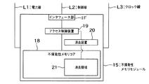
図1は、本発明の第1の実施の形態に従った不揮発性メモリモジュールの構成を概略的に示す図である。 FIG. 1 schematically shows a configuration of a nonvolatile memory module according to a first embodiment of the present invention.
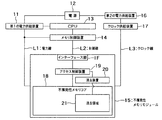
図2は、図1の不揮発性メモリモジュールを適用した不揮発性メモリシステムの構成を示す図である。 FIG. 2 is a diagram showing a configuration of a nonvolatile memory system to which the nonvolatile memory module of FIG. 1 is applied.
図2に示すように、第1の電力供給装置11は、電源12から供給される電力を用いて、CPU13、メモリ制御装置14及び不揮発性メモリモジュール15に供給する動作電圧(電力)を生成する。生成された電力は、電力線L1を介して、CPU13、メモリ制御装置14及び不揮発性メモリモジュール15に供給される。
As shown in FIG. 2, the first
第2の電力供給装置16は、電源12から供給される電力を用いて、クロック供給装置17への動作電圧(電力)を生成する。クロック供給装置17は、第2の電力供給装置16から供給された電力を用いて所定の周波数によるクロックを生成し、生成したクロックを、クロック線L3を介して、不揮発性メモリモジュール15に供給する。CPU13、メモリ制御装置14へのクロックは、クロック供給装置17から供給されるか、あるいは、図示しない別のクロック供給装置から供給される。
The second power supply device 16 generates an operating voltage (power) to the
CPU13は、与えられた各種命令を実行し、メモリ制御装置14は、CPU13による指示を受けて、制御線L2を介して、不揮発性メモリモジュール15における不揮発性メモリコア18にアクセスする。不揮発性メモリコア18は、例えばFeRAM、MRAM等の不揮発性RAMの他、種々の不揮発性のメモリを含み得る。メモリ制御装置14と不揮発性メモリモジュール15とはインターフェース部IFを介して接続される。
The
通常動作時においては、不揮発性メモリモジュール15におけるアクセス制御装置19は、メモリ制御装置14による不揮発性メモリコア18へのアクセスを許容する。即ち、データ書き込み時は、メモリ制御装置14は、CPU13によって指定されたアドレスに、指定のデータを書き込む。データ読み出し時は、メモリ制御装置14は、CPU13によって指定されたアドレスからデータを読み出してCPU13に渡す。
During normal operation, the
ここで、通常動作時は、不揮発性メモリモジュール15、CPU13及びメモリ制御装置14に電力及びクロックが供給された状態の時を示す。
Here, during normal operation, power and a clock are supplied to the nonvolatile memory module 15, the
これに対し、不揮発性メモリモジュール15に電力及びクロックが供給されていない状態から、電力及びクロックが供給された状態に遷移する時を、即ち、不揮発性メモリモジュール15が起動した時を、動作開始時(起動時)と称する。例えば、ユーザによる電源投入時がこの起動時に該当する。 In contrast, when the nonvolatile memory module 15 is not supplied with power and clock, the operation starts when the transition from the state where power and clock are supplied, that is, when the nonvolatile memory module 15 is activated. This is referred to as time (at startup). For example, the time when the user turns on the power corresponds to this start-up.
この起動時における動作について以下詳細に説明する。 The operation at the time of starting will be described in detail below.
起動時においては、不揮発性メモリモジュール15における消去装置20が、不揮発性メモリコア18における所定の消去領域21内のデータを消去する。即ち、消去装置20は、不揮発性メモリコア18に対する電力及びクロックの供給が停止状態から供給状態に遷移したことを検知した場合は、消去領域21内のデータを消去する。消去領域を特定する情報は、あらかじめアクセス制御装置19あるいは消去装置20内に格納されている。消去領域には、例えば個人情報、パスワード、著作権データ等が格納される。不揮発性メモリアコアの全領域を消去領域としても良い。消去領域を特定する情報は、上述の通常動作時において、例えばCPU13により変更可能であることが好ましい。
At startup, the
消去装置20によるデータ消去の間、アクセス制御装置19は、メモリ制御装置14から不揮発性メモリコア18へのアクセスを阻止する。例えば、データ消去の間に、メモリ制御装置14から不揮発性メモリコア18へのアクセス(書き込み、読み出し等)が発生した場合は、そのアクセス内容を、アクセス制御装置19が一時的に記憶する。
During the data erasure by the
消去装置20によるデータの消去が終了すると、消去装置20は、完了信号をアクセス制御装置19に出力し、アクセス制御装置19は、メモリ制御装置14から不揮発性メモリコア18へのアクセスを許容する(有効にする)。アクセス制御装置19が、消去装置20によるデータ消去の間に、メモリ制御装置14からのアクセス内容を記憶した場合は、そのアクセス内容を不揮発性メモリコア18に出力する。不揮発性メモリコア18は、そのアクセス内容に応じた処理を実行する。
When the
上述した不揮発性モジュール15は、アクセス制御装置19、消去装置20及び不揮発性メモリコア18が同一の半導体基板上に形成されることにより構成されてもよいし、それぞれあるいは任意の組み合わせが別個の半導体基板上に形成されてこれらが同一のパッケージに含まれる場合も含む。
The non-volatile module 15 described above may be configured by forming the
また、不揮発性メモリシステムは、例えば、不揮発性メモリモジュール15、第1の電力供給装置11及びクロック供給装置17がそれぞれ別個のチップとして構成される場合や、アクセス制御装置19、消去装置20、不揮発性メモリコア18、第1の電力供給装置及びクロック供給装置17の任意の組み合わせがそれぞれ別個のチップとして構成される場合、これらが同一のチップ上に形成される場合も含む。
In addition, the nonvolatile memory system includes, for example, a case where the nonvolatile memory module 15, the first
以上のように、本実施の形態によれば、不揮発性メモリモジュールの起動時、即ち、不揮発性メモリコアの起動時に、不揮発性メモリコアへのアクセスを不可としつつ、不揮発性メモリコア内のデータを消去するようにしたので、不揮発性メモリコア内のデータを第3者から有効に保護できる。例えば、不揮発性メモリモジュールが第3者によって不正にシステムから取り出された場合でも、電源投入時に、不揮発性メモリコア内のデータが自動的に消去されるので、第3者によって機密情報や著作権データ等が読み出されることを有効に防止できる。 As described above, according to the present embodiment, when the nonvolatile memory module is activated, that is, when the nonvolatile memory core is activated, data in the nonvolatile memory core is disabled while disabling access to the nonvolatile memory core. Since data is erased, data in the nonvolatile memory core can be effectively protected from a third party. For example, even if a non-volatile memory module is illegally removed from the system by a third party, the data in the non-volatile memory core is automatically deleted when the power is turned on. Reading data and the like can be effectively prevented.
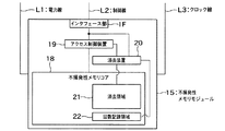
図3は、本発明の第2の実施の形態に従った不揮発性メモリモジュールの構成を示す図である。 FIG. 3 is a diagram showing a configuration of a nonvolatile memory module according to the second embodiment of the present invention.
上述した第1の実施の形態では、不揮発性メモリモジュール15が起動する度に、消去装置20によるデータの消去が実行されたが、本実施の形態では、不揮発性メモリモジュール15の起動が所定回数生じた時点で、データの消去が実行される。以下、本実施の形態について詳しく説明する。
In the first embodiment described above, data erasure is performed by the
図3に示すように、不揮発性メモリコア18内には、「残り起動回数」を示す数値を格納する回数記録領域22が配置される。不揮発性メモリモジュール15が起動する度に、消去装置20によってこの値が「1」減算される。そして、この値が「0」になると、消去装置20は、データの消去を実行する。
As shown in FIG. 3, in the
消去装置20は、データの消去を実行すると、回数記録領域22内に、所定の数値(使用回数制限値)を格納する。従って、例えば、データの消去の後、所定の数値として、「10」が格納された場合、この後、さらに起動が10回発生した時点で、再びデータの消去が実行される。
When erasing the data, the erasing
回数記録領域22内への数値の格納は、消去装置20が、通常動作時にCPU13から設定指示を受け、この設定指示に基づいて行うことも可能である。消去装置20は、CPU13からの設定指示を受けると、回数記録領域22内の数値を確認し、「0」であれば、設定指示に基づいて回数記録領域22内に数値を入力し、「0」でなければ、前回の設定を優先し、設定指示を実行しない。
The numerical value can be stored in the number-of-
以上のように、本実施の形態によれば、不揮発性メモリモジュールが所定の回数だけ起動したら、不揮発性メモリコア内のデータを消去するようにしたので、種々の事情を考慮したデータ消去機能の使用が可能になる。例えば、本不揮発性メモリモジュールを搭載した端末をあるサーバに接続する際にパスワードの入力を必要とする場合に、通常はメモリコアに記憶されたパスワードを用いて自動接続すると共に、定期的にメモリコア内のパスワードを消去することで、ユーザに定期的にパスワードの入力を求めることが可能となる。また、この端末をあるサーバに接続する回数を制限する場合では、その実装として、接続に必要な情報を消去対象とすることで、所定の回数起動後に接続できなくすることも考えられる。 As described above, according to this embodiment, when the nonvolatile memory module is activated a predetermined number of times, the data in the nonvolatile memory core is erased. Can be used. For example, when connecting a terminal equipped with the nonvolatile memory module to a server and entering a password, it is usually connected automatically using a password stored in the memory core and periodically By erasing the password in the core, it becomes possible to prompt the user to input the password periodically. Further, when limiting the number of times this terminal is connected to a certain server, as an implementation, it is conceivable that information necessary for connection can be erased so that connection cannot be made after a predetermined number of times of activation.
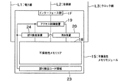
図4は、本発明の第3の実施の形態に従った不揮発性メモリモジュールの構成を示すブロック図である。 FIG. 4 is a block diagram showing a configuration of a nonvolatile memory module according to the third embodiment of the present invention.
図4に示すように、メモリ制御装置14(図2参照)は、不揮発性メモリコア18にデータを書き込む際、誤り検出コード領域23に誤り検出コードを格納する。この誤り検出コードは、後に不揮発性メモリコア18からデータを読み出した際、このデータに誤りが無いかどうか、即ち、書き込んだデータと読み出したデータとが一致しているか否かを検査するために用いるものである。誤り検出コードとしては、例えば書き込みデータから算出されるチェックサム等がある。このような誤り検出の手法は周知であるので、ここでは詳細な説明は省略する。
As shown in FIG. 4, the memory control device 14 (see FIG. 2) stores an error detection code in the error
誤り検査装置24は、不揮発性メモリモジュール15の起動時に、不揮発性メモリコア18内のデータに誤りが無いかを、誤り検出コード領域23内の誤り検出コードを用いて検査する。検査対象となるメモリ領域は、不揮発性メモリコア18内の全領域でもよいし、あらかじめ指定された領域でもよい。誤り検査装置24がこの検出処理を行っている間は、アクセス制御装置19は、メモリ制御回路14(図2参照)による不揮発性メモリコア18へのアクセスを阻止する。
The
誤り検査装置24は、データに誤りが無い場合は、その旨をアクセス制御装置19に送出し、アクセス制御装置19は、メモリ制御回路14(図2参照)から不揮発性メモリコア18へのアクセスを有効にする。
If there is no error in the data, the
一方、誤り検査装置24は、データ誤りが存在した場合は、誤りデータの格納されたメモリ領域を消去装置20に通知し、消去装置20は、そのメモリ領域内のデータを消去する。誤り検査装置24は、検査を終えると、その旨を消去装置20に通知し、消去装置20は、誤り検査装置24によって指定された全てのメモリ領域内のデータを消去したら、終了通知をアクセス制御装置19に送出する。アクセス制御装置19は、メモリ制御装置14(図2参照)による不揮発性メモリコア18へのアクセスを有効にする。
On the other hand, when there is a data error, the
以上のように、本実施の形態によれば、不揮発性メモリモジュールの起動時に不揮発性メモリコア内のデータに誤りがあるか否かを検査し、データに誤りがある場合は、少なくともそのデータを消去するようにしたので、不揮発性メモリコア内に誤ったデータを保持することによる問題を未然に防止できる。 As described above, according to the present embodiment, it is checked whether or not there is an error in the data in the nonvolatile memory core when the nonvolatile memory module is started up. Since the data is erased, problems caused by holding erroneous data in the nonvolatile memory core can be prevented.
例えば、ユーザを識別するコードが不揮発性メモリコアに格納されおり、ハードエラー等で、そのコードが、例えば他人の識別コードに変わったとする。もし、ユーザが、その状態で、そのコードに基づいて、認証を要するサーバにアクセスすると、そのユーザは不正アクセスであると判断される恐れがある。しかし、本実施の形態では、このようにデータが変わってしまった場合は、自動時にデータが消去されるので、このような問題を未然に防止できる。 For example, it is assumed that a code for identifying a user is stored in the nonvolatile memory core, and the code is changed to, for example, another person's identification code due to a hardware error or the like. If the user accesses a server that requires authentication based on the code in that state, the user may be determined to be unauthorized access. However, in this embodiment, when the data changes in this way, the data is erased at the time of automatic operation, so that such a problem can be prevented beforehand.
11 第1の電力供給装置
12 電源
13 CPU
14 メモリ制御装置
15 不揮発性メモリモジュール
16 第2の電力供給装置
17 クロック供給装置
18 不揮発性メモリコア
19 アクセス制御装置
20 消去装置
21 消去領域
22 回数記録領域
23 誤り検出コード領域
24 誤り検査装置
L1 電力線
L2 制御線
L3 クロック線
IF インターフェース部
11 First
14 Memory control device 15 Non-volatile memory module 16 Second
Claims (5)
前記不揮発性メモリに対する前記電力及び前記クロックの供給が停止状態から供給状態に遷移した場合は、前記不揮発性メモリ内のデータを消去する消去部と、
を備えた不揮発性メモリモジュール。 A non-volatile memory that operates using the supplied power and the supplied clock;
When the supply of the power and the clock to the nonvolatile memory transitions from a stopped state to a supply state, an erasing unit that erases data in the nonvolatile memory;
A non-volatile memory module.
前記不揮発性メモリ内のデータに誤りがあるか否かを検査するための誤り検出コードを格納したコード格納部と、
前記不揮発性メモリに対する前記電力及び前記クロックの供給が停止状態から供給状態に遷移した場合は、前記誤り検出コードを用いて、前記不揮発性メモリ内のデータに誤りがあるか否かを検査する検査部と、
検査の結果、前記不揮発性メモリ内のデータに誤りがある場合は、誤りのある前記データを消去する消去部と、
を備えた不揮発性メモリモジュール。 A non-volatile memory that operates using the supplied power and the supplied clock;
A code storage unit storing an error detection code for checking whether or not there is an error in the data in the nonvolatile memory;
When the supply of the power and the clock to the nonvolatile memory transits from a stopped state to a supply state, an inspection is performed to check whether there is an error in the data in the nonvolatile memory using the error detection code And
As a result of the inspection, if there is an error in the data in the nonvolatile memory, an erasing unit for erasing the erroneous data,
A non-volatile memory module.
前記不揮発性メモリに電力を供給する電力供給部と、
前記不揮発性メモリにクロックを供給するクロック供給部と、
前記不揮発性メモリに対する前記電力及び前記クロックの供給が停止状態から供給状態に遷移した場合は、前記不揮発性メモリ内のデータを消去する消去部と、
前記消去部による前記データの消去が行われている間は、前記不揮発性メモリへのアクセスを阻止するアクセス制御部と、
を備えた不揮発性メモリシステム。 Non-volatile memory;
A power supply unit for supplying power to the nonvolatile memory;
A clock supply unit for supplying a clock to the nonvolatile memory;
When the supply of the power and the clock to the nonvolatile memory transitions from a stopped state to a supply state, an erasing unit that erases data in the nonvolatile memory;
While the data is being erased by the erasing unit, an access control unit that blocks access to the nonvolatile memory;
A non-volatile memory system.
Priority Applications (1)
| Application Number | Priority Date | Filing Date | Title |
|---|---|---|---|
| JP2004103871A JP2005292959A (en) | 2004-03-31 | 2004-03-31 | Nonvolatile memory module and nonvolatile memory system |
Applications Claiming Priority (1)
| Application Number | Priority Date | Filing Date | Title |
|---|---|---|---|
| JP2004103871A JP2005292959A (en) | 2004-03-31 | 2004-03-31 | Nonvolatile memory module and nonvolatile memory system |
Publications (1)
| Publication Number | Publication Date |
|---|---|
| JP2005292959A true JP2005292959A (en) | 2005-10-20 |
Family
ID=35325857
Family Applications (1)
| Application Number | Title | Priority Date | Filing Date |
|---|---|---|---|
| JP2004103871A Pending JP2005292959A (en) | 2004-03-31 | 2004-03-31 | Nonvolatile memory module and nonvolatile memory system |
Country Status (1)
| Country | Link |
|---|---|
| JP (1) | JP2005292959A (en) |
Cited By (8)
| Publication number | Priority date | Publication date | Assignee | Title |
|---|---|---|---|---|
| JP2006235887A (en) * | 2005-02-24 | 2006-09-07 | Sanyo Electric Co Ltd | Content processing device |
| JP2007265096A (en) * | 2006-03-29 | 2007-10-11 | Hitachi Software Eng Co Ltd | Information leakage prevention method and removable media |
| JP2008040585A (en) * | 2006-08-02 | 2008-02-21 | Renesas Technology Corp | Microcomputer |
| WO2009087970A1 (en) * | 2008-01-11 | 2009-07-16 | Nidec Sankyo Corporation | Memory monitoring method |
| JP2011141888A (en) * | 2011-03-11 | 2011-07-21 | Renesas Electronics Corp | Single chip microcomputer |
| JP2012531687A (en) * | 2009-06-29 | 2012-12-10 | トムソン ライセンシング | Data security in solid state memory |
| JP2021520021A (en) * | 2018-04-23 | 2021-08-12 | マイクロン テクノロジー,インク. | Non-volatile memory devices and systems with non-volatile memory mechanisms and methods for operating them |
| US11769561B2 (en) | 2018-04-23 | 2023-09-26 | Micron Technology, Inc. | Non-volatile memory devices and systems with read-only memory features and methods for operating the same |
-
2004
- 2004-03-31 JP JP2004103871A patent/JP2005292959A/en active Pending
Cited By (11)
| Publication number | Priority date | Publication date | Assignee | Title |
|---|---|---|---|---|
| JP2006235887A (en) * | 2005-02-24 | 2006-09-07 | Sanyo Electric Co Ltd | Content processing device |
| US7669247B2 (en) | 2005-02-24 | 2010-02-23 | Sanyo Electric Co., Ltd. | Content processing apparatus |
| JP2007265096A (en) * | 2006-03-29 | 2007-10-11 | Hitachi Software Eng Co Ltd | Information leakage prevention method and removable media |
| JP2008040585A (en) * | 2006-08-02 | 2008-02-21 | Renesas Technology Corp | Microcomputer |
| WO2009087970A1 (en) * | 2008-01-11 | 2009-07-16 | Nidec Sankyo Corporation | Memory monitoring method |
| JP2009169550A (en) * | 2008-01-11 | 2009-07-30 | Nidec Sankyo Corp | Memory monitoring method |
| JP2012531687A (en) * | 2009-06-29 | 2012-12-10 | トムソン ライセンシング | Data security in solid state memory |
| JP2011141888A (en) * | 2011-03-11 | 2011-07-21 | Renesas Electronics Corp | Single chip microcomputer |
| JP2021520021A (en) * | 2018-04-23 | 2021-08-12 | マイクロン テクノロジー,インク. | Non-volatile memory devices and systems with non-volatile memory mechanisms and methods for operating them |
| US11495299B2 (en) | 2018-04-23 | 2022-11-08 | Micron Technology, Inc. | Non-volatile memory devices and systems with volatile memory features and methods for operating the same |
| US11769561B2 (en) | 2018-04-23 | 2023-09-26 | Micron Technology, Inc. | Non-volatile memory devices and systems with read-only memory features and methods for operating the same |
Similar Documents
| Publication | Publication Date | Title |
|---|---|---|
| US7761717B2 (en) | Memory device with data security in a processor | |
| USRE47621E1 (en) | Secure transaction microcontroller with secure boot loader | |
| JP4000654B2 (en) | Semiconductor device and electronic equipment | |
| US10509568B2 (en) | Efficient secure boot carried out in information processing apparatus | |
| CN100380348C (en) | Semiconductor device having encryption portion or external interface | |
| CN110020561B (en) | Semiconductor device and method of operating semiconductor device | |
| TW200832427A (en) | Virtual secure on-chip one time programming | |
| TWI405211B (en) | Flash memory storage system, controller and data protecting method thereof | |
| KR20010034283A (en) | Storage device, encrypting/decrypting device, and method for accessing nonvolatile memory | |
| US20030212871A1 (en) | Memory device and method of controlling the same | |
| JP2001005729A (en) | Non-volatile memory that prevents unauthorized reading | |
| JP5462453B2 (en) | Semiconductor device | |
| JP2005292959A (en) | Nonvolatile memory module and nonvolatile memory system | |
| US20050259465A1 (en) | Nonvolatile memory apparatus | |
| CN101218609B (en) | Portable data carrier with secure data processing | |
| US20040186947A1 (en) | Access control system for nonvolatile memory | |
| KR100830910B1 (en) | Semiconductor memory device | |
| JP4822231B2 (en) | Fault detection due to long perturbations | |
| JP2006146358A (en) | Usb peripheral equipment control system and usb peripheral equipment control method | |
| JP2007066008A (en) | Electronic device | |
| US7916549B2 (en) | Memory self-test circuit, semiconductor device and IC card including the same, and memory self-test method | |
| US20060289656A1 (en) | Portable electronic apparatus and data output method therefor | |
| JP4053245B2 (en) | Semiconductor memory device that can prevent unauthorized use | |
| JP2003203012A (en) | Microcomputer device | |
| US20260003517A1 (en) | Method for configuring a microcontroller and corresponding microcontroller |