JP2005292851A - Substrate for liquid crystal device, liquid crystal device and electronic apparatus - Google Patents
Substrate for liquid crystal device, liquid crystal device and electronic apparatus Download PDFInfo
- Publication number
- JP2005292851A JP2005292851A JP2005156732A JP2005156732A JP2005292851A JP 2005292851 A JP2005292851 A JP 2005292851A JP 2005156732 A JP2005156732 A JP 2005156732A JP 2005156732 A JP2005156732 A JP 2005156732A JP 2005292851 A JP2005292851 A JP 2005292851A
- Authority
- JP
- Japan
- Prior art keywords
- liquid crystal
- light
- crystal device
- substrate
- base material
- Prior art date
- Legal status (The legal status is an assumption and is not a legal conclusion. Google has not performed a legal analysis and makes no representation as to the accuracy of the status listed.)
- Granted
Links
Images


Landscapes
- Liquid Crystal (AREA)
Abstract
【課題】 反射光が不要な視野角方向へ進行することを防止して、希望する視野角方向へ向かう反射光の光量を増大させることにより、希望の方向から見たときの表示の明るさを増大させることのできる液晶装置用基板を提供する。
【解決手段】 液晶を挟持する一対の基板のうち観察側と反対側に位置する液晶装置用基板2aである。基材6aの表面に光反射膜としての画素電極9が形成される。光反射膜9の表面には複数の山部10cを並べて成るパターンが形成され、これらの山部10cは、自らを通る直交2軸線X,Yの一方の軸線に沿った立体形状と、他方の軸線に沿った立体形状とが互いに異なるように、長円形状のドーム形状に形成される。光反射膜9は光指向性及び光散乱性の両方の特性を実現する。
【選択図】 図2
PROBLEM TO BE SOLVED: To reduce the brightness of display when viewed from a desired direction by preventing the reflected light from traveling in an unnecessary viewing angle direction and increasing the amount of reflected light toward the desired viewing angle direction. Provided is a liquid crystal device substrate which can be increased.
A substrate 2a for a liquid crystal device located on the opposite side to an observation side of a pair of substrates sandwiching a liquid crystal. A pixel electrode 9 as a light reflecting film is formed on the surface of the substrate 6a. A pattern is formed on the surface of the light reflecting film 9 by arranging a plurality of crests 10c. The crests 10c have a three-dimensional shape along one of the two orthogonal axes X and Y passing through the crest 10c and the other crest 10c. It is formed in an oval dome shape so that the three-dimensional shape along the axis is different from each other. The light reflecting film 9 realizes both light directivity and light scattering characteristics.
[Selection] Figure 2
Description
本発明は、液晶装置の構成要素である液晶装置用基板に関する。また、本発明は、液晶装置用基板を用いて構成される液晶装置に関する。また、本発明は、液晶装置を用いて構成される電子機器に関する。 The present invention relates to a substrate for a liquid crystal device which is a component of the liquid crystal device. The present invention also relates to a liquid crystal device configured using a substrate for a liquid crystal device. The present invention also relates to an electronic apparatus configured using a liquid crystal device.
近年、携帯電話機、携帯型パーソナルコンピュータ等といった電子機器に液晶装置が広く用いられるようになってきている。この液晶装置の1つとして、反射型表示が可能な液晶装置が知られている。この液晶装置では、自然光や室内光等といった外部光が該液晶装置の内部へ取り込まれ、この光が該液晶装置の内部に設けた光反射膜で反射して再び外部へ出射することにより表示が行われる。 In recent years, liquid crystal devices have been widely used in electronic devices such as mobile phones and portable personal computers. As one of such liquid crystal devices, a liquid crystal device capable of reflective display is known. In this liquid crystal device, external light such as natural light or room light is taken into the liquid crystal device, and this light is reflected by a light reflecting film provided inside the liquid crystal device and emitted again to the outside. Done.
この構成によれば、バックライトすなわち照明装置を用いなくても表示が出来るので、消費電力を低く抑えることができる。また、バックライトを付設しない場合には薄型化及び軽量化を達成できる。 According to this configuration, since display can be performed without using a backlight, that is, a lighting device, power consumption can be suppressed low. In addition, when a backlight is not provided, a reduction in thickness and weight can be achieved.
この反射型表示が可能な液晶装置においては、光反射膜の表面が鏡面状であると、観察者が視認する像に背景や室内照明が映ってしまい、表示された像が見難くなるという問題が生じる。この問題を解消するため、従来、上記光反射膜の表面に複数の微細な山部を形成して粗面化して、反射光を適度に散乱させるという技術が知られている。 In a liquid crystal device capable of this reflective display, if the surface of the light reflecting film is mirror-like, the background or room illumination is reflected in the image visually recognized by the observer, and the displayed image becomes difficult to see Occurs. In order to solve this problem, conventionally, a technique is known in which a plurality of fine crests are formed on the surface of the light reflecting film to roughen the surface, and the reflected light is appropriately scattered.
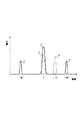
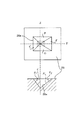
上記従来の液晶装置用基板における光反射面の粗面化によってもたらされる反射光は、光量が上下左右の全領域で均一になるように設定されていた。例えば、図17に示すように、液晶装置用基板91に法線方向から光R0を照射すると共に、ディテクタ例えばフォトマルチメータ92を直交2軸線であるX軸線及びY軸線の各方向へ移動させながら、反射光R1の光量を測定したところ、図18に示すように、X軸線方向における−90°〜+90°の範囲の反射光量プロファイルQX と、Y軸線方向における−90°〜+90°の範囲の反射光量プロファイルQY とは同じプロファイルとなっていた。
The reflected light caused by the roughening of the light reflecting surface in the conventional substrate for a liquid crystal device has been set so that the amount of light is uniform in all the upper, lower, left and right regions. For example, as shown in FIG. 17, the liquid
上記のような方向性の無い反射光は、液晶装置において均一な明るさの像を表示させるという観点から見れば有効であるが、液晶装置の表示面を常に特定の1つの方向から観察するような場合には、不要な視野角方向に光が供給される分だけ、光が無駄に費やされていたと考えられる。 Reflection light having no directivity as described above is effective from the viewpoint of displaying an image with uniform brightness in the liquid crystal device, but the display surface of the liquid crystal device is always observed from one specific direction. In such a case, it is considered that light was wasted as much as the light was supplied in an unnecessary viewing angle direction.
本発明は、上記の問題点に鑑みて成されたものであって、反射光が不要な視野角方向へ進行することを防止して、希望する視野角方向へ向かう反射光の光量を増大させることにより、希望の方向から見たときの表示の明るさを増大させることを目的とする。 The present invention has been made in view of the above problems, and prevents the reflected light from traveling in an unnecessary viewing angle direction and increases the amount of reflected light toward the desired viewing angle direction. Accordingly, it is an object to increase the brightness of the display when viewed from a desired direction.
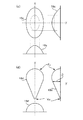
まず、本発明を原理的に説明する。今、図14(a)及び図14(b)に示すように基材81の表面に光反射膜82を形成し、その光反射膜82の表面に正四角錐形状すなわち正ピラミッド形状の複数の山部10をドットマトリクス状に配列した構造の基板80を考える。この場合、山部10は図15(a)に示すように、平面断面Tが正方形状で直交2軸線であるX軸線及びY軸線の両方に関して対称な形状であるとする。また、図15(a)において山部10の4つの側面を“A”、“B”、“C”及び“D”と呼び、また山部10が載っている基材表面を“E”と呼ぶことにする。
First, the principle of the present invention will be described. Now, as shown in FIGS. 14A and 14B, a
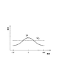
図14(b)に矢印Aで示すように、複数の山部10を形成した光反射膜82に対して光を照射したとき、図15(a)のY軸線方向に関する反射光量の分布を測定すると、図16に示すように、面積の広い平面Eに対応して光量の大きい反射光eが発生し、側面A及び側面Bに対応して適宜の角度、例えば±30°の所にそれらの面積に対応した光量の反射光a及びcが発生する。この光量分布はX軸線方向に関しても全く同じであり、この結果、図14(a)の基板80に光を照射すると、立体空間の全方位に方向性の無い均一な反射光が得られる。
As shown by an arrow A in FIG. 14B, when the
次に、図15(a)における山部10の側面AをY軸線方向の外側へ伸ばした形状の図15(b)に示すような山部10eを考える。すると、この山部10eに関しては側面A'の基材25に対する傾斜角度θ2は側面Cの傾斜角度θ1よりも小さくなり、さらに側面A'の面積は山部10における側面Aの面積よりも大きくなる。従って、この山部10eに光が照射されると、図16において、30°よりも小さい視野角度、例えば15°の視野角度の所に側面Aの場合よりも光量が少し大きい反射光a'が現れ、さらに、平面Eは面積が狭くなるので反射光e'はそれに対応して反射光の光量が少し小さくなる。
Next, let us consider a
つまり、山部10の形状をY軸線方向に変形させてX軸線に関して非対称の形にすると、Y軸線方向に関して特定の不要な視野角方向の反射光量を低減すると同時に、特定の希望する視野角方向の反射光量を意図的に増大させることができる。この結果、例えば本基板80を液晶装置の反射板として用いる場合を考えれば、観察者による視認方向以外の視野角方向の明るさを抑えた上で、観察者が見る視野角方向の明るさだけを意図的に強めることができる。
That is, if the shape of the
(1) 本発明は上記のような原理に基づいて成されたものであって、本発明に係る液晶装置用基板は、液晶を挟持する一対の基板のうち観察側と反対側に位置する液晶装置用基板において、基材と、該基材の表面に形成された光反射膜とを有し、該光反射膜は光指向性及び光散乱性を呈するパターンを有することが望ましい。 (1) The present invention is made on the basis of the principle as described above, and the substrate for a liquid crystal device according to the present invention is a liquid crystal positioned on the opposite side to the observation side of a pair of substrates holding the liquid crystal. The apparatus substrate preferably includes a base material and a light reflecting film formed on the surface of the base material, and the light reflecting film has a pattern exhibiting light directivity and light scattering properties.
今、一般的な光の反射を考えると、図19に示すように反射面Hに角度θ0で入射した光R0は、等しい角度θ0で反射する。この場合には、反射面Hは、光指向性を呈することも無く、光散乱性を呈することも無い。上記構成における「光指向性」とは、図19において、反射光の主たる成分R1が入射角度θ0とは異なる角度θ1で反射するという特性である。また、「光散乱性」とは、角度θ2から角度θ3の範囲で散乱光が発生するという特性である。 Considering general reflection of light, as shown in FIG. 19, light R0 incident on the reflecting surface H at an angle θ0 is reflected at an equal angle θ0. In this case, the reflecting surface H does not exhibit light directivity and does not exhibit light scattering. The “light directivity” in the above configuration is a characteristic that the main component R1 of the reflected light is reflected at an angle θ1 different from the incident angle θ0 in FIG. The “light scattering property” is a characteristic that scattered light is generated in the range of the angle θ2 to the angle θ3.
主反射光の角度θ1は、散乱角度であるθ2からθ3の範囲内に入る場合もあるし、入らない場合もある。しかしながら、多くの場合、主反射角度θ1は散乱角度範囲であるθ2からθ3の内部に入るように設定され、さらに、望ましくは主反射角度θ1は散乱角度θ2からθ3の中心になるように設定される。液晶装置の場合には、θ2からθ3の角度差を約30°に設定し、全反射光量の60%以上がこの角度範囲内に存在するように設定することが望ましい。 The angle θ1 of the main reflected light may or may not fall within the range of the scattering angle θ2 to θ3. However, in many cases, the main reflection angle θ1 is set to be within the scattering angle range θ2 to θ3, and more preferably, the main reflection angle θ1 is set to be the center of the scattering angles θ2 to θ3. The In the case of a liquid crystal device, it is desirable to set the angle difference between θ2 and θ3 to about 30 °, and to set so that 60% or more of the total reflected light amount exists within this angle range.
上記構成の液晶装置用基板によれば、反射光R1の反射角度θ1が入射角度θ0以外の角度値に設定されるので、希望する視野角方向へ向かう反射光の光量を増大させることができ、これにより、希望の方向から見たときの表示の明るさを増大させることができる。 According to the liquid crystal device substrate having the above configuration, since the reflection angle θ1 of the reflected light R1 is set to an angle value other than the incident angle θ0, it is possible to increase the amount of reflected light toward the desired viewing angle direction, Thereby, the brightness of the display when viewed from a desired direction can be increased.
上記構成の液晶装置において、前記パターンは複数の山部及び/又は複数の谷部を並べて形成できる。また、それらの山部及び/又は谷部は、自らを通る直交2軸線の一方の軸線に沿った立体形状と、他方の軸線に沿った立体形状とが互いに異なるように形成できる。 In the liquid crystal device having the above configuration, the pattern can be formed by arranging a plurality of peaks and / or a plurality of valleys. Moreover, these peak parts and / or trough parts can be formed so that the three-dimensional shape along one axis of two orthogonal axes passing through itself and the three-dimensional shape along the other axis line are different from each other.
本発明に関わる液晶装置用基板は、液晶を挟持する一対の基板のうち観察側と反対側に位置する液晶装置用基板において、基材と、該基材上に形成された光反射膜とを有し、該光反射膜は光指向性及び光散乱性を呈するパターンを有し、前記パターンは、尖った一端と緩やかに曲がる他端とを結んだ平面形状を有する液滴形状の複数の山部を並べて設けられてなり、前記山部は、前記基材に直交する面であって、且つそれぞれが前記液滴形状の頂点に接するとともに、互いに直交する2つの面の断面形状が互いに異なることを特徴とする。 A substrate for a liquid crystal device according to the present invention is a substrate for a liquid crystal device located on the opposite side to the observation side of a pair of substrates sandwiching liquid crystal, and includes a base material and a light reflecting film formed on the base material. The light reflecting film has a pattern exhibiting light directivity and light scattering, and the pattern has a plurality of droplet-shaped peaks having a planar shape connecting one sharp end and the other gently curved end. The crests are surfaces that are orthogonal to the base material, and are in contact with the top of the droplet shape, and the cross-sectional shapes of the two surfaces that are orthogonal to each other are different from each other. It is characterized by.
本発明に関わる液晶装置用基板は、液晶を挟持する一対の基板のうち観察側と反対側に位置する液晶装置用基板において、基材と、該基材上に形成された光反射膜とを有し、該光反射膜は光指向性及び光散乱性を呈するパターンを有し、前記パターンは液滴形状の複数の谷部を並べて設けられてなり、前記谷部は、前記基材に直交する面であって、且つそれぞれが前記液滴形状の最深部に接するとともに、互いに直交する2つの面の断面形状が互いに異なることを特徴とする。 A substrate for a liquid crystal device according to the present invention is a substrate for a liquid crystal device located on the opposite side to the observation side of a pair of substrates sandwiching liquid crystal, and includes a base material and a light reflecting film formed on the base material. The light reflecting film has a pattern exhibiting light directivity and light scattering, and the pattern is formed by arranging a plurality of droplet-shaped valleys, and the valleys are orthogonal to the substrate. Each of which is in contact with the deepest portion of the droplet shape, and the cross-sectional shapes of two surfaces orthogonal to each other are different from each other.
例えば、光反射膜の表面に多数のドットパターンとして形成する山部は、図11(a)に示すように平面断面が長方形状で例えばX軸線方向に長いドーム型の山部10aや、図11(b)に示すように平面断面が長方形状で例えばX軸線方向に長い四角錐形状すなわちピラミッド形状の山部10bや、図12(c)に示すように平面断面が長円形状で例えばX軸線方向に長いドーム型の山部10c等のように形成できる。
For example, the crest formed as a large number of dot patterns on the surface of the light reflecting film has a rectangular cross section as shown in FIG. 11A and has a
また、山部は、図12(d)に示すように平面形状が液滴形状の山部10dのように形成できる。ここで、液滴形状というのは、尖った一端E0と緩やかに曲がる他端E1とを略直線で結んだ平面形状を有し、且つ尖った先端E0から緩やかに曲がる他端E1にかけて徐々に寸法D、この場合には山の高さD、が大きくなる断面形状を有する形状である。
Further, as shown in FIG. 12D, the peak portion can be formed like a
また、光反射膜の表面に多数のドットパターンとして形成する谷部は、図20(a)に示すように平面断面が長方形状で例えばX軸線方向に長いドーム型の谷部20aや、図20(b)に示すように平面断面が長方形状で例えばX軸線方向に長い四角錐形状すなわちピラミッド形状の谷部20bや、図21(c)に示すように平面断面が長円形状で例えばX軸線方向に長いドーム型の谷部20c等のように形成できる。
In addition, the valley formed as a large number of dot patterns on the surface of the light reflecting film has a rectangular cross section as shown in FIG. 20A, for example, a dome-shaped
また、谷部は、図21(d)に示すように平面形状が液滴形状の谷部20dのように形成できる。ここで、液滴形状というのは、尖った一端E0と緩やかに曲がる他端E1とを略直線で結んだ平面形状を有し、且つ尖った先端E0から緩やかに曲がる他端E1にかけて徐々に寸法D、この場合は谷の深さD、が大きくなる断面形状を有する形状である。
Further, as shown in FIG. 21 (d), the valley portion can be formed like a
上記構成の液晶装置用基板によれば、光反射膜は入射した光を立体空間の全方位へ均一に反射するのではなく、特定の視野方向の光量又は強度が強くなるように反射する。これにより、反射光が不要な視野角方向へ進行することを防止して、希望する視野角方向へ向かう反射光の光量を増大させることができ、希望の方向から見たときの表示の明るさを増大させることができる。 According to the substrate for a liquid crystal device having the above configuration, the light reflecting film does not uniformly reflect the incident light in all directions of the three-dimensional space, but reflects the light amount or intensity in a specific viewing direction. This prevents the reflected light from traveling in an unnecessary viewing angle direction, and can increase the amount of reflected light toward the desired viewing angle direction. The brightness of the display when viewed from the desired direction Can be increased.
次に、上記構成の液晶装置用基板において、前記山部及び/又は前記谷部は、自らを通る直交2軸線のうちの少なくとも一方の軸線によって区分される一方の側の立体形状と他方の側の立体形状とが互いに非対称となるように形成できる。 Next, in the substrate for a liquid crystal device having the above-described configuration, the crest and / or the trough are divided into a three-dimensional shape on one side and the other side separated by at least one of the two orthogonal axes passing through the crest and / or the trough. These three-dimensional shapes can be asymmetric with each other.
本発明に関わる液晶装置用基板は、液晶を挟持する一対の基板のうち観察側と反対側に位置する液晶装置用基板において、基材と、該基材上に形成された光反射膜とを有し、該光反射膜は光指向性及び光散乱性を呈するパターンを有し、前記パターンは、尖った一端と緩やかに曲がる他端とを結んだ平面形状を有する液滴形状の複数の山部を並べて設けられてなり、前記山部は、前記基材に直交する面であって、且つそれぞれが前記液滴形状の頂点に接するとともに、互いに直交する2つの面のうちの少なくとも一方の面によって区分される一方の側の立体形状と他方の側の立体形状とが互いに非対称であることを特徴とする。 A substrate for a liquid crystal device according to the present invention is a substrate for a liquid crystal device located on the opposite side to the observation side of a pair of substrates sandwiching liquid crystal, and includes a base material and a light reflecting film formed on the base material. The light reflecting film has a pattern exhibiting light directivity and light scattering, and the pattern has a plurality of droplet-shaped peaks having a planar shape connecting one sharp end and the other gently curved end. The crests are surfaces that are orthogonal to the base material and that are in contact with the top of the droplet shape and that are at least one of the two surfaces orthogonal to each other. The three-dimensional shape on one side and the three-dimensional shape on the other side which are separated by the above are asymmetric with each other.
本発明に関わる液晶装置用基板は、液晶を挟持する一対の基板のうち観察側と反対側に位置する液晶装置用基板において、基材と、該基材上に形成された光反射膜とを有し、該光反射膜は光指向性及び光散乱性を呈するパターンを有し、前記パターンは液滴形状の複数の谷部を並べて設けられてなり、前記谷部は、前記基材に直交する面であって、且つそれぞれが前記液滴形状の最深部に接するとともに、互いに直交する2つの面のうちの少なくとも一方の面によって区分される一方の側の立体形状と他方の側の立体形状とが互いに非対称であることを特徴とする。 A substrate for a liquid crystal device according to the present invention is a substrate for a liquid crystal device located on the opposite side to the observation side of a pair of substrates sandwiching liquid crystal, and includes a base material and a light reflecting film formed on the base material. The light reflecting film has a pattern exhibiting light directivity and light scattering, and the pattern is formed by arranging a plurality of droplet-shaped valleys, and the valleys are orthogonal to the substrate. A solid shape on one side and a solid shape on the other side, each of which is in contact with the deepest portion of the droplet shape and is divided by at least one of the two surfaces orthogonal to each other Are asymmetric with each other.
例えば、光反射膜の山部は、図15(b)に示すように、1つの側面A'が対向する側面Cよりも面積が広く且つ基材25に対する傾斜角度が側面Cよりも小さい大きさの角錐形状すなわちピラミッド形状10eとすることができる。この形状では、X軸線によって区分される左部の立体形状と右部の立体形状とが互いに非対称になっている。
For example, as shown in FIG. 15B, the peak portion of the light reflecting film has a larger area than the side surface C on which one side surface A ′ faces, and an inclination angle with respect to the
また、光反射膜の山部は、図12(d)に示すように、一方の軸線であるY軸線によって区分される上部の立体形状と下部の立体形状とが互いに非対称となるように形成することもできる。 Further, as shown in FIG. 12 (d), the peak portion of the light reflecting film is formed so that the upper three-dimensional shape and the lower three-dimensional shape, which are separated by one of the Y axes, are asymmetrical to each other. You can also
また、光反射膜の谷部は、図22に示すように、1つの側面A'が対向する側面Cよりも面積が広く且つ基材25に対する傾斜角度が側面Cよりも小さい大きさの角錐形状すなわちピラミッド形状20eとすることができる。この形状では、X軸線によって区分される左部の立体形状と右部の立体形状とが互いに非対称になっている。また、光反射膜の谷部は、図21(d)に示すように、一方の軸線であるY軸線によって区分される上部の立体形状と下部の立体形状とが互いに非対称となるように形成することもできる。
Further, as shown in FIG. 22, the valley portion of the light reflecting film has a pyramid shape having a larger area than the side surface C facing one side surface A ′ and a smaller inclination angle with respect to the
上記構成の液晶装置用基板によれば、光反射膜は入射した光を立体空間の全方位へ均一に反射するのではなく、特定の方向の光量又は強度が強くなるように反射する。これにより、反射光が不要な視野角方向へ進行することを防止して、希望する視野角方向へ向かう反射光の光量を増大させることができ、希望の方向から見たときの表示の明るさを増大させることができる。 According to the substrate for a liquid crystal device having the above-described configuration, the light reflecting film does not uniformly reflect the incident light in all directions of the three-dimensional space, but reflects the light quantity or intensity in a specific direction. This prevents the reflected light from traveling in an unnecessary viewing angle direction, and can increase the amount of reflected light toward the desired viewing angle direction. The brightness of the display when viewed from the desired direction Can be increased.
上記構成の液晶装置用基板において、軸線によって区分される部分の立体形状を該軸線に関して非対称にするという構成要件は、例えば、面積に関して非対称にしたり、基材に対する角度に関して非対称にしたりする等といった具体例が考えられる。面積に関して非対称にすることは、例えば図15(b)の山部10eのようにX軸線の左側面Cの面積と右側面A'の面積とを異ならせることや、例えば図22の谷部20eのようにX軸線の左側面Cの面積と右側面A'の面積とを異ならせることによって実現できる。
In the liquid crystal device substrate having the above configuration, the configuration requirement that the three-dimensional shape of the portion divided by the axis is asymmetric with respect to the axis is, for example, asymmetric with respect to the area or asymmetric with respect to the angle with respect to the substrate. Examples are possible. To make the area asymmetrical, for example, the area of the left side surface C of the X-axis and the area of the right side surface A ′ are different as in the
また、角度に関して非対称にすることは、例えば図15(b)の山部10eのようにX軸線の左側面Cの基材25に対する角度θ1と右側面A'の基板25に対する角度θ2とを異ならせることや、例えば図22の谷部20eのようにX軸線の左側面Cの基材25に対する角度θ1と右側面A'の基板25に対する角度θ2とを異ならせることによって実現できる。
Further, making the angle asymmetric means that the angle θ1 of the left side surface C of the X axis with respect to the
次に、上記構成の液晶装置用基板においては、山部及び/又は谷部の形状を特定するための直交2軸線の少なくとも一方が前記基材の端辺に平行であることが望ましい。これにより、複数の山部及び/又は複数の谷部の配列から成る光散乱パターンの基材に対する配置が一義的に決められ、その結果、基材をどの方向から見れば明るい表示となるかに関する判断が容易にできるようになる。 Next, in the substrate for a liquid crystal device having the above-described configuration, it is desirable that at least one of the two orthogonal axes for specifying the shape of the crest and / or trough is parallel to the edge of the substrate. As a result, the arrangement of the light scattering pattern consisting of an array of a plurality of peaks and / or a plurality of valleys is uniquely determined, and as a result, from which direction the substrate is viewed, a bright display is obtained. Judgment can be made easily.
次に、上記構成の液晶装置用基板において、前記複数の山部及び/又は前記複数の谷部は互いに同じ方向で且つ平面内で無秩序に並べられることが望ましい。また、本発明の基板において反射光に指向性を持たせるためには、複数の山部が互いに同じ方向を向いていることが重要である。また、光の干渉等といった不要な光学現象の発生を防止するためには、複数の山部を平面内で無秩序、すなわちランダムに並べることが望ましい。 Next, in the substrate for a liquid crystal device having the above-described configuration, it is preferable that the plurality of crests and / or the plurality of troughs are arranged in a random manner in the same direction and in a plane. Further, in order to give the reflected light directivity in the substrate of the present invention, it is important that the plurality of peak portions are directed in the same direction. Further, in order to prevent the occurrence of unnecessary optical phenomena such as light interference, it is desirable to arrange a plurality of crests randomly, that is, randomly.
次に、本発明に係る液晶装置用基板は、液晶を挟持する一対の基板のうち観察側と反対側に位置する液晶装置用基板であって、基材と、該基材の表面に形成された光反射膜とを有し、該光反射膜の表面には複数の山部及び/又は谷部を並べて成る光反射パターンが形成され、該光反射パターンで反射する光の光量に関して、前記山部及び/又は谷部を通る直交2軸線の一方に沿った光量プロファイルと、直交2軸線の他方に沿った光量プロファイルとが互いに異なることが望ましい。 Next, the substrate for a liquid crystal device according to the present invention is a substrate for a liquid crystal device located on the side opposite to the observation side of a pair of substrates that sandwich the liquid crystal, and is formed on the base material and the surface of the base material. A light reflection pattern formed by arranging a plurality of peaks and / or valleys on the surface of the light reflection film, and the amount of light reflected by the light reflection pattern It is desirable that the light amount profile along one of the two orthogonal axes passing through the portion and / or the valley is different from the light amount profile along the other of the two orthogonal axes.
本発明に関わる液晶装置用基板は、液晶を挟持する一対の基板のうち観察側と反対側に位置する液晶装置用基板において、基材と、該基材上に形成された光反射膜とを有し、該光反射膜には、尖った一端と緩やかに曲がる他端とを結んだ平面形状を有する液滴形状の複数の山部を並べて成る光反射パターンが形成され、該光反射パターンで反射する光の光量に関して、前記基材に直交する面であって、且つそれぞれが前記液滴形状の頂点に接するとともに、互いに直交する2つの面において、法線方向から入射した光の前記2つの面のうちの一方の面に沿った反射光量の変化と、前記2つの面のうちの他方の面に沿った反射光量の変化とが互いに異なることを特徴とする。
本発明に関わる液晶装置用基板は、液晶を挟持する一対の基板のうち観察側と反対側に位置する液晶装置用基板において、基材と、該基材上に形成された光反射膜とを有し、該光反射膜には液滴形状の複数の谷部を並べて成る光反射パターンが形成され、該光反射パターンで反射する光の光量に関して、前記基材に直交する面であって、且つそれぞれが前記液滴形状の最深部に接するとともに、互いに直交する2つの面において、法線方向から入射した光の前記2つの面のうちの一方の面に沿った反射光量の変化と、前記2つの面のうちの他方の面に沿った反射光量の変化とが互いに異なることを特徴とする。
A substrate for a liquid crystal device according to the present invention is a substrate for a liquid crystal device located on the opposite side to the observation side of a pair of substrates sandwiching liquid crystal, and includes a base material and a light reflecting film formed on the base material. The light reflecting film is formed with a light reflecting pattern formed by arranging a plurality of droplet-shaped crests having a planar shape connecting one sharp end and the other end that bends gently. Regarding the amount of light to be reflected, the two surfaces of the light incident from the normal direction on two surfaces that are orthogonal to the substrate and are in contact with the top of the droplet shape and orthogonal to each other. A change in the amount of reflected light along one of the surfaces is different from a change in the amount of reflected light along the other of the two surfaces.
A substrate for a liquid crystal device according to the present invention is a substrate for a liquid crystal device located on the opposite side to the observation side of a pair of substrates sandwiching liquid crystal, and includes a base material and a light reflecting film formed on the base material. The light reflecting film is formed with a light reflecting pattern in which a plurality of droplet-shaped valleys are arranged, and with respect to the amount of light reflected by the light reflecting pattern, the light reflecting film is a surface orthogonal to the substrate, And the change in the amount of reflected light along one of the two surfaces of the light incident from the normal direction on two surfaces that are in contact with the deepest part of the droplet shape and orthogonal to each other, and The change in the amount of reflected light along the other surface of the two surfaces is different from each other.
この構成の液晶装置用基板によれば、光反射膜は入射した光を立体空間の全方位へ均一に反射するのではなく、特定の方向の光量又は強度が強くなるように反射する。これにより、反射光が不要な視野角方向へ進行することを防止して、希望する視野角方向へ向かう反射光の光量を増大させることができ、希望の方向から見たときの表示の明るさを増大させることができる。 According to the substrate for a liquid crystal device having this configuration, the light reflecting film does not uniformly reflect the incident light in all directions of the three-dimensional space, but reflects the light quantity or intensity in a specific direction. This prevents the reflected light from traveling in an unnecessary viewing angle direction, and can increase the amount of reflected light toward the desired viewing angle direction. The brightness of the display when viewed from the desired direction Can be increased.
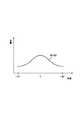
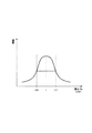
例えば、図17に示す測定系で反射光の光量を測定したとき、得られるプロファイルが図13に示すように、一方の軸線に沿った光量プロファイルQyは山形状であり、前記他方の軸線に沿った光量プロファイルQxは直線状であるといったような特性を有する光反射パターンにより、上記構成の液晶装置用基板を実現できる。 For example, when the amount of reflected light is measured by the measurement system shown in FIG. 17, the obtained profile is as shown in FIG. 13, and the light amount profile Qy along one axis is mountain-shaped, and along the other axis. The liquid crystal device substrate having the above-described configuration can be realized by a light reflection pattern having such a characteristic that the light quantity profile Qx is linear.
本発明の液晶装置用基板は、前記一方の面に沿った反射光量の変化は山形状であり、前記他方の面に沿った反射光量の変化は直線状であることを特徴とする。
図13に示す特性を有する液晶装置用基板を用いれば、Y方向に沿って目を移動させたときには、中央部が明るく両端部が暗い表示が視認できる。一方、X方向に沿って目を移動させたときには、一方の端部から他方の端部にわたって均一な明るさの表示を見ることができる。X方向に沿った見え方とY方向に沿った見え方とを比べれば、X方向に沿った見え方は両端部側、すなわち低角度側から表示面を見たときの明るさが増大する。
前記一方の面に沿った反射光量の変化は山形状であり、前記他方の面に沿った反射光量の変化は直線状であることを特徴とする液晶装置用基板。
The substrate for a liquid crystal device according to the present invention is characterized in that the change in the amount of reflected light along the one surface is mountain-shaped, and the change in the amount of reflected light along the other surface is linear.
When the liquid crystal device substrate having the characteristics shown in FIG. 13 is used, when the eyes are moved along the Y direction, a display in which the central portion is bright and both end portions are dark can be visually recognized. On the other hand, when the eyes are moved along the X direction, a display with uniform brightness can be seen from one end to the other end. If the appearance along the X direction is compared with the appearance along the Y direction, the brightness along the X direction increases the brightness when the display surface is viewed from both ends, that is, from the low angle side.
The change in the amount of reflected light along the one surface has a mountain shape, and the change in the amount of reflected light along the other surface is linear.
また、本発明に関わる液晶装置用基板の液滴形状は、尖った一端と緩やかに曲がる他端とを結んだ平面形状を有することを特徴とする。 In addition, the liquid crystal device substrate according to the present invention is characterized in that the droplet shape has a planar shape connecting a sharp end and a gently bent other end.
本発明に関わる液晶装置用基板の前記山部の頂点は、前記一端よりも前記他端に寄せて配置されてなることを特徴とする。
本発明に関わる液晶装置用基板の前記谷部の最深部は、前記一端よりも前記他端に寄せて配置されてなることを特徴とする。
The peak of the peak portion of the substrate for a liquid crystal device according to the present invention is arranged closer to the other end than the one end.
The deepest part of the valley of the substrate for a liquid crystal device according to the present invention is arranged closer to the other end than the one end.
(2) 次に、本発明に係る液晶装置用基板の製造方法は、液晶を挟持する一対の基板のうち観察側と反対側に位置する液晶装置用基板の製造方法において、基材の表面に光反射膜を形成する工程と、マスクを用いて前記光反射膜の表面に複数の山部及び/又は複数の谷部を形成する工程とを有し、前記複数の山部及び/又は複数の谷部に対応する前記マスクのマスクパターンは、自らを通る直交2軸線の一方の軸線に沿った形状と、他方の軸線に沿った形状とが互いに異なることが望ましい。この構成の液晶装置用基板の製造方法によれば、上記の液晶装置用基板を確実に製造することができる。 (2) Next, a method for manufacturing a substrate for a liquid crystal device according to the present invention is the method for manufacturing a substrate for a liquid crystal device located on the opposite side to the observation side of the pair of substrates holding the liquid crystal. A step of forming a light reflecting film, and a step of forming a plurality of peaks and / or a plurality of valleys on the surface of the light reflecting film using a mask, the plurality of peaks and / or a plurality of peaks It is desirable that the mask pattern of the mask corresponding to the trough is different in shape along one axis of two orthogonal axes passing through itself and the shape along the other axis. According to the method for manufacturing a substrate for a liquid crystal device having this structure, the substrate for a liquid crystal device can be reliably manufactured.
次に、本発明に係る液晶装置用基板の製造方法は、液晶を挟持する一対の基板のうち観察側と反対側に位置する液晶装置用基板の製造方法において、基材の表面に光反射膜を形成する工程と、マスクを用いて前記光反射膜の表面に複数の山部及び/又は複数の谷部を形成する工程とを有し、前記複数の山部及び/又は複数の谷部に対応する前記マスクのマスクパターンは、自らを通る直交2軸線のうちの少なくとも一方の軸線によって区分される一方の側の形状と他方の側の形状とが互いに非対称であることが望ましい。この構成の液晶装置用基板の製造方法によれば、上記の液晶装置用基板を確実に製造することができる。 Next, a method for manufacturing a substrate for a liquid crystal device according to the present invention is the method for manufacturing a substrate for a liquid crystal device located on the opposite side to the observation side of a pair of substrates sandwiching a liquid crystal. And a step of forming a plurality of peaks and / or a plurality of valleys on the surface of the light reflecting film using a mask, the plurality of peaks and / or the valleys In the mask pattern of the corresponding mask, it is desirable that the shape on one side and the shape on the other side which are separated by at least one of the two orthogonal axes passing through the mask are asymmetric with each other. According to the method for manufacturing a substrate for a liquid crystal device having this structure, the substrate for a liquid crystal device can be reliably manufactured.
上記構成の液晶装置用基板の製造方法において、前記複数の山部及び/又は複数の谷部に対応する前記マスクのマスクパターンは平面的な液滴形状とすることができる。ここで、平面的な液滴形状とは、尖った一端と緩やかに曲がる他端とを略直線で結んだ平面形状である。また、上記構成の液晶装置用基板の製造方法において、前記複数の山部及び/又は複数の谷部に対応する前記マスクのマスクパターンは互いに同じ方向で且つ平面内で無秩序に並べることができる。 In the method for manufacturing a substrate for a liquid crystal device having the above-described configuration, the mask pattern of the mask corresponding to the plurality of peak portions and / or the plurality of valley portions may have a planar droplet shape. Here, the planar droplet shape is a planar shape in which one sharp end and the other end that bends gently are connected by a substantially straight line. In the method for manufacturing a substrate for a liquid crystal device having the above-described configuration, the mask patterns of the mask corresponding to the plurality of peaks and / or the plurality of valleys can be randomly arranged in the same direction and in a plane.
(3) 次に、本発明に係る液晶装置は、液晶を挟持する一対の基板を有する液晶装置において、該一対の基板の一方は、以上に説明した各種構成の液晶装置用基板によって構成されることを特徴とする。 (3) Next, the liquid crystal device according to the present invention is a liquid crystal device having a pair of substrates that sandwich the liquid crystal, and one of the pair of substrates is configured by the liquid crystal device substrate having various configurations described above. It is characterized by that.
この構成の液晶装置によれば、内部の反射膜で反射して液晶層に供給される光の反射角度を当該光の液晶装置への入射角度以外の角度値に設定できるので、希望する視野角方向へ向かう反射光の光量を増大させることができ、これにより、液晶装置の表示面を希望の方向から見たときの表示の明るさを増大させることができる。 According to the liquid crystal device of this configuration, the reflection angle of the light reflected by the internal reflection film and supplied to the liquid crystal layer can be set to an angle value other than the incident angle of the light to the liquid crystal device, so that the desired viewing angle The amount of reflected light directed in the direction can be increased, whereby the brightness of the display when the display surface of the liquid crystal device is viewed from a desired direction can be increased.
(4) 次に、本発明に係る液晶装置の製造方法は、液晶を挟持する一対の基板を有する液晶装置の製造方法において、以上に説明した液晶装置用基板の製造方法を用いて前記一対の基板の一方を形成する工程を有することが望ましい。 (4) Next, a method for manufacturing a liquid crystal device according to the present invention is the method for manufacturing a liquid crystal device having a pair of substrates that sandwich a liquid crystal. It is desirable to have a step of forming one of the substrates.
(5) 次に、本発明に係る電子機器は、像を表示する液晶装置と、該液晶装置を収容する筐体と、前記液晶装置を制御する制御回路とを有する電子機器において、前記液晶装置は、以上に記載した構成の液晶装置によって構成されることを特徴とする。この電子機器によれば、液晶装置の表示を見る者にとって、好ましい視野角方向に鮮明な像を形成することができる。 (5) Next, an electronic apparatus according to the present invention is an electronic apparatus including a liquid crystal device that displays an image, a casing that houses the liquid crystal device, and a control circuit that controls the liquid crystal device. Is constituted by the liquid crystal device having the above-described configuration. According to this electronic apparatus, a clear image can be formed in a viewing angle direction preferable for a person who views the display of the liquid crystal device.
以下、本発明を実施形態に基づいて、より具体的に説明する。 Hereinafter, the present invention will be described more specifically based on embodiments.
(液晶装置用基板及び液晶装置の第1実施形態)
図1及び図2は、本発明に係る液晶装置用基板を用いた本発明に係る液晶装置の一実施形態の主要部、特に1つの表示ドット部分を拡大して示している。この液晶装置の全体構造は例えば図3に示すように設定できる。なお、例えば、R(赤)、G(緑)、B(青)の3原色によってフルカラー表示を行う場合を考えれば、上記の1つの表示ドットはそれら3色の個々に対応するドットであり、これらの表示ドットが3個集まることによって1つの画素が形成される。また、白黒表示を行う場合を考えれば、上記の1つの表示ドットがそのまま1つの画素に相当する。
(First Embodiment of Substrate for Liquid Crystal Device and Liquid Crystal Device)
1 and 2 show an enlarged view of a main part, in particular, one display dot portion, of an embodiment of a liquid crystal device according to the present invention using the substrate for a liquid crystal device according to the present invention. The overall structure of the liquid crystal device can be set as shown in FIG. 3, for example. For example, considering a case where full color display is performed with three primary colors of R (red), G (green), and B (blue), the one display dot is a dot corresponding to each of the three colors, One pixel is formed by collecting these three display dots. Considering the case of performing black and white display, the one display dot corresponds to one pixel as it is.
本実施形態に係る液晶装置は、アクティブ素子として3端子型の能動素子であるTFT(Thin Film Transistor)を用いたアクティブマトリクス方式の液晶装置であり、自然光等といった外部光を用いて表示を行う方式の反射型液晶装置であり、そして液晶駆動用ICを基板上に直接に実装する方式のCOG(Chip On Glass)方式の液晶装置である。 The liquid crystal device according to the present embodiment is an active matrix type liquid crystal device using a TFT (Thin Film Transistor) which is a three-terminal type active element as an active element, and performs a display using external light such as natural light. And a COG (Chip On Glass) liquid crystal device in which a liquid crystal driving IC is directly mounted on a substrate.
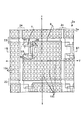
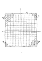
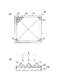
図3において、液晶装置1は第1基板2aと第2基板2bとをそれらの周辺部において環状のシール材3によって貼り合わせ、さらに、第1基板2a、第2基板2b及びシール材3によって囲まれる間隙すなわちセルギャップ内に液晶を封入することによって形成される。また、本実施形態では、一方の基板2aの表面に液晶駆動用IC4a及び4bが直接に実装されている。
In FIG. 3, the liquid crystal device 1 includes a
第1基板2aのシール材3によって囲まれる内部領域には、複数の画素電極が行方向XX及び列方向YYに関してドットマトリクス状の配列で形成される。また、第2基板2bのシール材3によって囲まれる内部領域には、無パターンの面状電極が形成され、その面状電極が第1基板2a側の複数の画素電極に対向して配置される。
In the inner region surrounded by the sealing material 3 of the
第1基板2a上の1つの画素電極と第2基板2b上の面状電極によって液晶を挟んだ部分が1つの表示ドットを形成し、この表示ドットの複数個がシール材3によって囲まれる内部領域内でドットマトリクス状に配列することによって表示領域Vが形成される。液晶駆動用IC4a及び4bは複数の表示ドットを形成している対向電極間に選択的に走査信号及びデータ信号を印加することにより、液晶の配向を表示ドット毎に制御する。この液晶の配向制御により該液晶を通過する光が変調されて、表示領域V内に文字、数字等といった像が表示される。
An internal region in which a liquid crystal is sandwiched between one pixel electrode on the
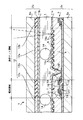
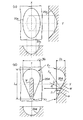
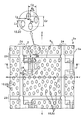
図1は、液晶装置1において表示領域Vを構成する複数の表示ドットのうちの1つの断面構造を拡大して示している。また、図2は、その表示ドットの平面構造を示している。なお、図1は図2におけるI−I線に従った断面構造を示している。 FIG. 1 shows an enlarged cross-sectional structure of one of a plurality of display dots constituting the display region V in the liquid crystal device 1. FIG. 2 shows the planar structure of the display dots. FIG. 1 shows a cross-sectional structure according to the line II in FIG.
図1において、第1基板2aは、ガラス、プラスチック等によって形成された基材6aと、その基材6a上に形成されたスイッチング素子として機能するアクティブ素子としてのTFT(Thin Film Transistor)7と、有機絶縁膜8を挟んでTFT7の上層に形成された画素電極9とを有する。画素電極9の上には配向膜11aが形成され、この配向膜11aに対して配向処理としてのラビング処理が施される。画素電極9は、例えばAl(アルミニウム)、Ag(銀)等といった光反射性の導電材料によって形成される。
In FIG. 1, a
第1基板2aに対向する第2基板2bは、ガラス、プラスチック等によって形成された基材6bと、その基材6b上に形成されたカラーフィルタ12と、そのカラーフィルタ12の上に形成された透明な電極13と、その電極13の上に形成された配向膜11bとを有する。電極13は、ITO(Indium Tin Oxide)等によって基材6bの表面全域に形成された面電極である。
The
カラーフィルタ12は、第1基板2a側の画素電極9に対向する位置にR(赤),G(緑),B(青)又はC(シアン),M(マゼンタ),Y(イエロー)等といった各色のいずれかの色フィルタエレメント12aを有し、画素電極9に対向しない位置にブラックマスク12bを有する。
The
図1において、第1基板2aと第2基板2bとの間の間隔、すなわちセルギャップはいずれか一方の基板の表面に分散された球状のスペーサ14によって寸法が維持され、そのセルギャップ内に液晶Lが封入される。
In FIG. 1, the distance between the
TFT7は、基材6a上に形成されたゲート電極16と、このゲート電極16の上で基材6aの全域に形成されたゲート絶縁膜17と、このゲート絶縁膜17を挟んでゲート電極16の上方位置に形成された半導体層18と、その半導体層18の一方の側にコンタクト電極19を介して形成されたソース電極21と、さらに半導体層18の他方の側にコンタクト電極19を介して形成されたドレイン電極22とを有する。
The
図2に示すように、ゲート電極16はゲートバス配線23から延びている。また、ソース電極21はソースバス配線24から延びている。ゲートバス配線23は基材6aの横方向に延びていて縦方向へ等間隔で平行に複数本形成される。また、ソースバス配線24はゲート絶縁膜17(図1参照)を挟んでゲートバス配線23と交差するように縦方向へ延びていて横方向へ等間隔で平行に複数本形成される。
As shown in FIG. 2, the
ゲートバス配線23は図3の液晶駆動用IC4a及び4bの一方に接続されて例えば走査線として作用し、他方、ソースバス配線24は液晶駆動用IC4a及び4bの他方に接続されて例えば信号線として作用する。また、画素電極9は、図2に示すように、互いに交差するゲートバス配線23とソースバス配線24とによって区画される方形領域のうちTFT7に対応する部分を除いた領域を覆うように形成される。
The
ゲートバス配線23及びゲート電極16は、例えばクロム、タンタル等によって形成される。ゲート絶縁膜17は、例えば窒化シリコン(SiNX)、酸化シリコン(SiOX)等によって形成される。半導体層18は、例えばa−Si、多結晶シリコン、CdSe等によって形成される。コンタクト電極19は、例えばa−Si等によって形成される。ソース電極21及びそれと一体なソースバス配線24並びにドレイン電極22は、例えばチタン、モリブデン、アルミニウム等によって形成される。
The
図1に示す有機絶縁膜8は、ゲートバス配線23、ソースバス配線24及びTFT7を覆って基材6a上の全域に形成されている。但し、有機絶縁膜8のドレイン電極22に対応する部分にはコンタクトホール26が形成され、このコンタクトホール26の所で画素電極9とTFT7のドレイン電極22との導通がなされている。有機絶縁膜8のうち画素電極9が形成される領域には、例えば、図12(c)に示すような長円形状でドーム形状の山部10cが互いに微小間隔で規則的に、本実施形態では規則的なマトリクス状の配列となるように形成されている。この結果、有機絶縁膜8の上に積層される画素電極9も同様にして複数の山部10cの配列から成る光反射パターンを有することになる。
The organic
上記の山部10cは、図2において、ソースバス配線24の延在方向であるX軸線方向を長軸とし、それと直角なY軸線方向を短軸となるように配列されている。また、山部10cの長軸方向Xは図3において基材6aのXX方向に延びる端辺に対して平行に設定され、短軸方向Yは基材6aのYY方向に延びる端辺に対して平行に設定されている。このように、山部10cを規定するX,Y軸線方向と液晶装置1の基板6a等の端辺方向XX,YYとの間に関連付けをしておけば、どの視野角度方向から液晶装置1の表示領域Vを見たときに明るい表示を見ることができるかを、容易に判断できる。
In FIG. 2, the
本実施形態では、画素電極9を、例えばAl(アルミニウム)、Ag(銀)等といった光反射性の導電材料によって形成することにより、当該画素電極9を光反射膜として機能させている。また、その画素電極9の表面に複数の山部10cから成る反射パターンを設けたので、画素電極9は図19に示すような、光指向性及び光散乱性の両方を呈する反射パターンとして機能する。
In the present embodiment, the
本実施形態の液晶装置1は以上のように構成されているので、図1において、観察者側すなわち第2基板2b側から液晶装置1の内部へ入った外部光は、液晶Lを通過して光反射性材料によって形成された画素電極9に到達し、該電極9で反射して再び液晶Lへ供給される。液晶Lは、走査信号及びデータ信号によって選択される画素電極9と対向電極13との間に印加される電圧によって表示ドット毎にその配向が制御され、これにより、液晶Lに供給された反射光は表示ドット毎に変調され、これにより観察者側に文字、数字等といった像が表示される。
Since the liquid crystal device 1 of the present embodiment is configured as described above, in FIG. 1, external light that enters the liquid crystal device 1 from the viewer side, that is, the
本実施形態では、光反射膜として作用する画素電極9の表面に複数の山部10cを規則的に配列して成る反射パターンが形成されると共に、それら複数の山部10cはX軸線に沿った立体形状とY軸線に沿った立体形状とが互いに異なっているので、一定の視野角方向への反射光量を低く抑えた上で、別の特定の視野角方向への反射光量を増大させることができる。この結果、観察者は、液晶装置1の表示領域V内に表示される像を特定の視野角方向から非常に明るい表示として観察できる。
In the present embodiment, a reflection pattern is formed by regularly arranging a plurality of
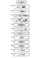
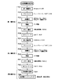
(液晶装置の製造方法の第1実施形態)
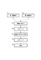
図4は、図1等に示した液晶装置1の製造方法を工程順に示している。この工程図に基づいて液晶装置1の製造方法を説明すれば、まず、工程P1において第1基板2a(図1参照)を作製し、工程P2において第2基板2bを作製する。通常の製造工程では、図3に示す液晶装置1の1個分の第1基板2a及び第2基板2bを1個ずつ作製するのではなく、1つの大面積の基材、いわゆるマザーボードの表面に液晶装置の複数個分の第1基板2aを形成し、他の1つのマザーボードの表面に液晶装置の複数個分の第2基板2bを形成する。
(First Embodiment of Manufacturing Method of Liquid Crystal Device)
FIG. 4 shows a manufacturing method of the liquid crystal device 1 shown in FIG. If the manufacturing method of the liquid crystal device 1 is described based on this process drawing, first, the
その後、複数の第1基板パターンが形成された第1基板マザーボードと、複数の第2基板パターンが形成された第2基板マザーボードとを互いに位置合わせ、すなわちアライメントした状態でシール材3によって貼り合わせて、大面積の空のパネル構造を形成する(工程P3)。次に、各液晶装置1内のシール材3の一部に形成された液晶注入口3a(図3参照)が外部に露出するように、上記大面積のパネル構造をブレイクすなわち切断して、いわゆる短冊状のパネル構造を形成する(工程P4)。
Thereafter, the first substrate motherboard on which the plurality of first substrate patterns are formed and the second substrate motherboard on which the plurality of second substrate patterns are formed are aligned with each other, that is, bonded together with the sealing material 3 in an aligned state. Then, an empty panel structure with a large area is formed (process P3). Next, the large-area panel structure is broken or cut so that a liquid
次に、作製された短冊状のパネル構造の液晶注入口3aからパネル構造の内部に液晶を注入し、さらに注入完了後の液晶注入口3aを樹脂によって封止する(工程P5)。その後、液晶封入後の短冊状のパネル構造を図3に示すような1個の液晶装置1の大きさにブレイクすなわち切断し(工程P6)、さらに液晶駆動用IC4a及び4bを一方の基板の表面に実装する(工程P7)。さらに、第1基板2a及び第2基板2bの外側表面に偏光板を貼着し、さらに必要に応じてその他の光学要素、例えば位相差板等を取り付け、これにより、図3の液晶装置1が完成する。
Next, liquid crystal is injected into the inside of the panel structure from the liquid
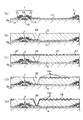
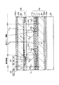
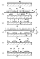
上記のような液晶装置の製造方法において、特に、第1基板形成工程P1は例えば図5に示す製造方法によって実現される。具体的には、工程P11及び図6(a)において、ガラス等から成る基材6aの上に、例えばスパッタリング法によってタンタル金属膜を形成し、この金属膜を例えばフォトリソグラフィー法によってパターニングして、ゲートバス配線23及びそれと一体なゲート電極16を形成する。
In the liquid crystal device manufacturing method as described above, in particular, the first substrate forming step P1 is realized by the manufacturing method shown in FIG. Specifically, in Step P11 and FIG. 6A, a tantalum metal film is formed on the
次に、工程P12及び図6(a)において、例えばプラズマCVD法によって窒化シリコンから成るゲート絶縁膜17を形成する。次に、工程P13及び図6(a)において、半導体層18となるa−Si層と、コンタクト電極19となるn+型a−Si層とをこの順で連続的に形成し、さらに、形成されたn+型a−Si層及びa−Si層のパターニングを行って半導体層18及びコンタクト電極19とを形成する。
Next, in Step P12 and FIG. 6A, a
次に、工程P14及び図6(a)において、基材6aの表面の全域に例えばモリブデン金属をスパッタ法によって形成し、このモリブデン金属層のパターニングを行って、ソース電極21、ドレイン電極22及びソースバス配線24を形成し、これによりTFT7が完成する。次に、工程P15及び図6(b)において、TFT7を形成した基材6a上の全面に例えばポリイミド樹脂をスピンコートして有機絶縁膜8を形成する。
Next, in Step P14 and FIG. 6A, for example, molybdenum metal is formed on the entire surface of the
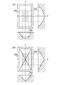
次に、工程16及び図6(b)において、フォトリソグラフィー法を用いて有機絶縁膜8にコンタクトホール26を形成する。次に、工程P17及び図6(c)において、有機絶縁膜8の上にフォトレジスト27を塗布し、図7に示すようなマスク28を用いて画素電極9の形成領域のフォトレジスト27をパターニングする。このときに用いるマスク28には、X軸線方向に長軸を有し、それと直角なY軸線方向に短軸を有する長円形状のマスクパターン29が形成される。
Next, in
次に、工程18及び図6(d)において、フォトレジスト27の無い部分の有機絶縁膜8をエッチングによって除去して規則的に並ぶ山部10cを形成する。このとき、コンタクトホール26及びTFT7の上の有機絶縁膜8はフォトレジスト27によって保護されてエッチングによって除去されない。エッチング処理後、フォトレジスト27は薬品や光照射によって除去される。
Next, in
その後、工程P19及び図6(e)において、有機絶縁膜8の上の全域にアルミニウム層を形成し、さらにパターニングして光反射膜を兼ねる画素電極38を形成する。このとき、画素電極38の下地となる有機絶縁膜8の表面に山部10cのパターンが形成されているので、画素電極38も同様の山部10cを有するパターン、すなわち光反射パターンを有することになる。画素電極38は有機絶縁膜26に形成されたコンタクトホール26を介してTFT7のドレイン電極22に接続される。
Thereafter, in step P19 and FIG. 6E, an aluminum layer is formed over the entire area of the organic insulating
その後、工程P20において基材8の表面の全域にポリイミド樹脂を塗布及び焼成することによって配向膜11a(図1参照)を形成し、それにラビング処理を施し、さらに工程P21においてスクリーン印刷等を用いてシール材3(図3参照)を形成し、さらに工程P22においてスペーサ14(図1参照)を分散し、これにより第1基板2aが完成する。
Thereafter, an
なお、以上の実施形態では図7のマスクパターン29として図12(c)に示す断面長円形ドーム形状の山部10cを形成できるパターンを用いたが、これに代えて、図11(a)に示す断面長方形ドーム形状や、図11(b)に示す断面長方形ピラミッド形状や、図12(d)に示す液滴ドーム形状や、図15(b)に示す断面長方形で偏形のピラミッド形状や、図13に示すように直交2軸線方向で光量分布が異なるような形状を採用することができる。
In the above embodiment, the
(液晶装置用基板及び液晶装置の第2実施形態)
図8は、本発明に係る液晶装置用基板を用いた本発明に係る液晶装置の他の実施形態の主要部、特に数個の表示ドット部分を拡大して示している。この液晶装置の全体構造は例えば図3に示すように設定できる。
(Second Embodiment of Liquid Crystal Device Substrate and Liquid Crystal Device)
FIG. 8 is an enlarged view of a main part of another embodiment of the liquid crystal device according to the present invention using the substrate for a liquid crystal device according to the present invention, particularly several display dot portions. The overall structure of the liquid crystal device can be set as shown in FIG. 3, for example.
本実施形態に係る液晶装置は、アクティブ素子として2端子型の能動素子であるTFD(Thin Film Diode)を用いたアクティブマトリクス方式の液晶装置であり、自然光等といった外部光を用いた反射表示と照明装置を用いた透過表示を選択的に行うことができる方式の半透過反射型液晶装置であり、そして液晶駆動用ICを基板上に直接に実装する方式のCOG(Chip On Glass)方式の液晶装置である。 The liquid crystal device according to the present embodiment is an active matrix type liquid crystal device using a TFD (Thin Film Diode) which is a two-terminal active element as an active element, and includes reflective display and illumination using external light such as natural light. COG (Chip On Glass) type liquid crystal device that is a transflective liquid crystal device that can selectively perform transmissive display using the device, and that has a liquid crystal driving IC mounted directly on a substrate It is.
本実施形態においても液晶装置1は、図3において、第1基板2aと第2基板2bとをシール材3によって貼り合わせ、さらに、第1基板2a、第2基板2b及びシール材3によって囲まれる間隙すなわちセルギャップ内に液晶を封入することによって形成される。また、一方の基板2aの表面に液晶駆動用IC4a及び4bが直接に実装されている。
Also in the present embodiment, the liquid crystal device 1 is bonded to the
第2基板2bのシール材3によって囲まれる内部領域には、複数の画素電極が行方向XX及び列方向YYに関してドットマトリクス状の配列で形成される。また、第1基板2aのシール材3によって囲まれる内部領域にはストライプ状の電極が形成され、そのストライプ状電極が第2基板2b側の複数の画素電極に対向して配置される。
In the inner region surrounded by the sealing material 3 of the
第1基板2a上のストライプ状電極と第2基板2b上の1つの画素電極によって液晶を挟んだ部分が1つの表示ドットを形成し、この表示ドットの複数個がシール材3によって囲まれる内部領域内でドットマトリクス状に配列することによって表示領域Vが形成される。液晶駆動用IC4a及び4bは複数の表示ドット内の対向電極間に選択的に走査信号及びデータ信号を印加することにより、液晶の配向を表示ドット毎に制御する。この液晶の配向制御により該液晶を通過する光が変調されて、表示領域V内に文字、数字等といった像が表示される。
A portion in which the liquid crystal is sandwiched between the striped electrode on the
図8は、液晶装置1において表示領域Vを構成する複数の表示ドットのうちの数個の断面構造を拡大して示している。また、図9は、1つの表示ドット部分の断面構造を示している。 FIG. 8 is an enlarged view of several cross-sectional structures among a plurality of display dots constituting the display region V in the liquid crystal device 1. FIG. 9 shows a cross-sectional structure of one display dot portion.
図8において、第1基板2aは、ガラス、プラスチック等によって形成された基材6aと、その基材6aの内側表面に形成された光反射膜31と、その光反射膜31の上に形成されたカラーフィルタ12と、そのカラーフィルタ12の上に形成された透明なストライプ状電極13とを有する。そのストライプ状電極13の上には図9に示すように配向膜11aが形成される。この配向膜11aに対して配向処理としてのラビング処理が施される。ストライプ状電極13は、例えばITO(Indium Tin Oxide)等といった透明な導電材料によって形成される。
In FIG. 8, the
第1基板2aに対向する第2基板2bは、ガラス、プラスチック等によって形成された基材6bと、その基材6bの内側表面に形成されたスイッチング素子として機能するアクティブ素子としてのTFD(Thin Film Diode)37と、TFD37に接続された画素電極9とを有する。TFD37及び画素電極9の上には図9に示すように配向膜11bが形成され、この配向膜11bに対して配向処理としてのラビング処理が施される。画素電極9は、例えばITO(Indium Tin Oxide)等といった透明な導電材料によって形成される。
The
第1基板2aに属するカラーフィルタ12は、第2基板2b側の画素電極9に対向する位置にR(赤),G(緑),B(青)又はC(シアン),M(マゼンタ),Y(イエロー)等といった各色のいずれかの色フィルタエレメント12aを有し、画素電極9に対向しない位置にブラックマスク12bを有する。
The
図9において、第1基板2aと第2基板2bとの間の間隔、すなわちセルギャップはいずれか一方の基板の表面に分散された球状のスペーサ14によって寸法が維持され、そのセルギャップ内に液晶Lが封入される。
In FIG. 9, the distance between the
TFD37は、図9及び図10に示すように、第1金属層34と、その第1金属層34の表面に形成された絶縁層36と、その絶縁層36の上に形成された第2金属層38とによって構成されている。このようにTFD37は、第1金属層/絶縁層/第2金属層から成る積層構造、いわゆるMIM(Metal Insulator Metal)構造によって構成されている。
As shown in FIGS. 9 and 10, the
第1金属層34は、例えば、タンタル単体、タンタル合金等によって形成される。第1金属層34としてタンタル合金を用いる場合には、主成分のタンタルに、例えば、タングステン、クロム、モリブデン、レニウム、イットリウム、ランタン、ディスプロリウム等といった周期律表において第6〜第8族に属する元素が添加される。
The
第1金属層34はライン配線39の第1層39aと一体に形成される。このライン配線39は画素電極9を間に挟んでストライプ状に形成され、画素電極9へ走査信号を供給するための走査線又は画素電極9へデータ信号を供給するためのデータ線として作用する。
The
絶縁層36は、例えば、陽極酸化法によって第1金属層34の表面を酸化することによって形成された酸化タンタル(Ta2O3)によって構成される。なお、第1金属層34を陽極酸化したときには、ライン配線39の第1層39aの表面も同時に酸化されて、同様に酸化タンタルから成る第2層39bが形成される。
The insulating
第2金属層38は、例えばCr等といった導電材によって形成される。画素電極9は、その一部が第2金属層38の先端に重なるように基材6bの表面に形成される。なお、基材6bの表面には、第1金属層34及びライン配線の第1層39aを形成する前に酸化タンタル等によって下地層を形成することがある。これは、第2金属層38の体積後における熱処理によって第1金属層34が下地から剥離しないようにしたり、第1金属層34に不純物が拡散しないようにしたりするためである。
The
図8において、基材6aの外側表面には位相差板32aが貼着等によって装着され、さらにその位相差板32aの上に偏光板33aが貼着等によって装着される。また、基材6bの外側表面には位相差板32bが貼着等によって装着され、さらにその位相差板32bの上に偏光板33bが貼着等によって装着される。
In FIG. 8, a
例えばSTN(Super Twisted Nematic)液晶等を用いると、該液晶を通過する光に波長分散が発生して表示像に着色が発生することがある。位相差板32a及び32bはそのような着色を除去するために用いられる光学的異方体であり、例えばポリビニルアルコール、ポリエステル、ポリエーテルアミド、ポリエチレン等といった樹脂を一軸延伸処理することによって形成されるフィルムによって構成できる。
For example, when STN (Super Twisted Nematic) liquid crystal or the like is used, wavelength dispersion may occur in the light passing through the liquid crystal, and the display image may be colored. The
偏光板33a及び33bは、自然光の入射に対してある一方向の直線偏光を出射する機能を有するフィルム状光学要素であり、例えば、偏光層をTAC(三酢酸セルロース)の保護層で挟むことによって形成できる。偏光板33a及び3bは、通常は、互いの透過偏光軸を異ならせて配置する。
The
光反射膜31は、例えば、アルミニウム等といった光反射性の金属によって形成され、第2基板2bに属する各画素電極9に対応する位置、すなわち各表示ドットに対応する位置に光透過用の開口41が形成される。また、光反射膜31の液晶側表面には、例えば、図12(c)に示すような長円形状でドーム形状の山部10cが互いに微小間隔で規則的に、本実施形態では規則的なマトリクス状の配列となるように形成されている。
The
上記の山部10cは、ライン配線39の延在方向であるX軸線方向を長軸とし、それと直角なY軸線方向が短軸となるように配列されている。また、山部10cの長軸方向Xは図3において基材6aのXX方向に延びる端辺に対して平行に設定され、短軸方向Yは基材6aのYY方向に延びる端辺に対して平行に設定されている。
The
本実施形態の液晶装置1は以上のように構成されているので、当該液晶装置1が反射型表示を行う場合には、図8において、観察者側すなわち第2基板2b側から液晶装置1の内部へ入った外部光は、液晶Lを通過して光反射膜31に到達し、該反射膜31で反射して再び液晶Lへ供給される(図9の矢印F1参照)。液晶Lは、画素電極9とストライプ状対向電極13との間に印加される電圧、すなわち走査信号及びデータ信号によって表示ドット毎にその配向が制御され、これにより、液晶Lに供給された反射光は表示ドット毎に変調され、これにより観察者側に文字、数字等といった像が表示される。
Since the liquid crystal device 1 of the present embodiment is configured as described above, when the liquid crystal device 1 performs reflective display, the liquid crystal device 1 of the liquid crystal device 1 is viewed from the observer side, that is, the
他方、液晶装置1が透過型表示を行う場合には、第1基板2aの外側に配置された照明装置、いわゆるバックライト42が発光し、この発光が偏光板33a、位相差板32a、基材6a、光反射膜31の開口41、カラーフィルタ12、電極13及び配向膜11aを通過した後に液晶Lに供給される(図9の矢印F2参照)。この後、反射型表示の場合と同様にして表示が行われる。
On the other hand, when the liquid crystal device 1 performs a transmissive display, an illumination device arranged outside the
本実施形態では、光反射膜31の表面に複数の山部10cを規則的に配列して成る反射パターンが形成されると共に、それら複数の山部10cはX軸線に沿った立体形状とY軸線に沿った立体形状とが互いに異なっているので、一定の視野角方向への反射光量を低く抑えた上で、別の特定の視野角方向への反射光量を増大させることができる。この結果、観察者は、光反射膜31を用いて行われる反射型表示の際に、液晶装置1の表示領域V内に表示される像を特定の視野角方向に関して非常に明るい表示として観察できる。
In the present embodiment, a reflection pattern formed by regularly arranging a plurality of
本実施形態の液晶装置1は、既に説明した図4に示す製造方法によって製造することができる。また、第1基板2a及び第2基板2bの形成方法も従来周知の方法を採用できる。なお、図8において第1基板2aの表面に光反射膜31を形成し、さらにその光反射膜に開口41及び反射パターンとしての山部10cを形成する際には、例えば、図7に示すような長円形状のマスクパターン29を縦横のマトリクス状に配列して成るマスク28を用いて行われるフォトリソグラフィー法を採用することができる。
The liquid crystal device 1 of the present embodiment can be manufactured by the manufacturing method shown in FIG. Also, a conventionally known method can be adopted as a method of forming the
なお、上記実施形態では図7のマスクパターン29として図12(c)に示す平面断面が長円形状でドーム形状の山部10cを形成できるパターンを用いたが、これに代えて、図11(a)に示すような平面断面が長方形状でドーム形状の山部10aや、図11(b)に示すような平面断面が長方形状でピラミッド形状の山部10bや、図12(d)に示すような液滴ドーム形状の山部10dや、図15(b)に示すような平面断面が長方形状で偏ったピラミッド形状の山部や、図13に示すように直交2軸線方向で光量分布が異なるような山部等を形成できる各種パターンを採用することができる。
In the above embodiment, the
なお、図1に示す実施形態では、光反射膜として作用する画素電極9の表面状態に関して、隣り合う山部10c同士の間に、図面上、鮮明な平坦部が形成されている。また、図9に示す実施形態では、光反射膜31の表面状態に関して、隣り合う山部10c同士の間に、図面上、鮮明な平坦部が形成されている。しかしながら、実際の山部形成工程においては、そのような鮮明な平坦部が形成されることは稀であり、多くの場合は図25に示すように、山部10c同士の間は平坦でない湾曲形状に形成されると考えられる。本発明のように、光反射膜によって光指向性及び光散乱性を実現しようとする場合、特に光散乱性を達成するためには、山部同士の間が鮮明な平坦面であるよりは、かえって上記のように山部同士の間が湾曲形状になっていた方が好ましいと考えられる。平坦面では鏡面反射が生じるので光散乱の程度が低くなるからである。
In the embodiment shown in FIG. 1, with respect to the surface state of the
(液晶装置用基板及び液晶装置の第3実施形態)
図1に示した液晶装置1では、光反射膜として作用する画素電極9に図12(c)に示した山部10cのような山部を複数個並べて成るパターンを、光指向性及び光散乱性を呈するパターンとして形成した。また、図8に示した液晶装置1では、そのような山部を複数個並べて成るパターンを光指向性及び光散乱性を呈するパターンとして光反射膜31に形成した。
(3rd Embodiment of the board | substrate for liquid crystal devices, and a liquid crystal device)
In the liquid crystal device 1 shown in FIG. 1, the
しかしながら、本発明に係る液晶装置用基板、液晶装置、電子機器及びそれらの製造方法においては、光指向性及び光散乱性を呈するパターンとして、複数の山部を並べて成るパターンに代えて、複数の谷部を並べて成るパターンを光指向性及び光散乱性を呈するパターンとして光反射膜に形成することができる。 However, in the substrate for a liquid crystal device, the liquid crystal device, the electronic device, and the manufacturing method thereof according to the present invention, instead of a pattern formed by arranging a plurality of peaks as a pattern exhibiting light directivity and light scattering, a plurality of A pattern formed by arranging valleys can be formed on the light reflecting film as a pattern exhibiting light directivity and light scattering.
具体的には、例えば、図20(a)に示すような平面断面が長方形状でドーム形状の谷部20aや、図20(b)に示すような平面断面が長方形状でピラミッド形状の谷部20bや、図21(c)に示すような平面断面が長円形状でドーム形状の谷部20cや、図21(d)に示すような液滴形状の谷部20dや、図22に示すような平面断面が長方形状でY軸線方向に偏ったピラミッド形状の谷部20eや、図13に示すように直交2軸線方向で光量分布が異なるような谷部等といった各種の谷部を複数個並べることによって光指向性及び光散乱性を呈するパターンを形成することができる。
Specifically, for example, a
なお、図20、図21及び図22において、X軸線及びY軸線は、図11等に示した山部10a等の場合と同様にして、それぞれが、図3のXX方向及びYY方向に一致していることが望ましい。
20, 21, and 22, the X-axis line and the Y-axis line correspond to the XX direction and the YY direction in FIG. 3 in the same manner as in the case of the
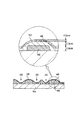
また、図21(d)に示した液滴形状の谷部20dは、尖った一端E0と緩やかに曲がる他端E1とを略直線で結んだ平面形状を有し、且つ尖った先端E0から緩やかに曲がる他端E1にかけて徐々に寸法D、この場合は谷の深さD、が大きくなる断面形状を有する形状である。
Further, the droplet-shaped
この液滴形状の谷部20dに関しては、先端E0から他端E1にかけて存在する領域Wにおいて、光源Sから出た光が角度2θで反射する傾向があり、これが、光反射膜の光指向性を決定する大きな因子となっている。そして、この場合のθは、とりもなおさず、先端E0から他端E1にかけての傾斜角度θということである。
With respect to the droplet-shaped
以上の結果、光源Sを太陽光、室内光等といった外部光と考え、反射角度2θの反射光の先(パネル表示面の法線方向)に観察者の目が位置すると考えれば、液晶装置の表示面を観察者が見たときに外部光によって最も効率良く表示された、明るくて鮮明な像を観察者によって視認できると考えられる。 As a result of the above, if the light source S is considered to be external light such as sunlight or room light, and the viewer's eyes are positioned ahead of the reflected light having a reflection angle 2θ (the normal direction of the panel display surface), the liquid crystal device It is considered that a bright and clear image displayed most efficiently by external light when the viewer looks at the display surface can be visually recognized by the viewer.
今、携帯電話機やその他の電子機器において、外部光と視認角度との間の上記の2θの反射角度を考えると、2θ=15°程度が実用的な角度であると思われる。このような2θ角度を実現するためには、谷部20dにおける先端E0から他端E1にかけての傾斜角度θをθ=15°/2=7.5°に設定すれば良い。
Now, in the cellular phone and other electronic devices, when the above 2θ reflection angle between the external light and the viewing angle is considered, about 2θ = 15 ° seems to be a practical angle. In order to realize such a 2θ angle, the inclination angle θ from the tip E0 to the other end E1 in the
また、発明者の実験によれば、液滴形状の谷部20dに関しては、その深さD0が約1μm、その幅W0が約9μm、そして、その長さL0が約14μmの場合に、好ましい光指向性及び光散乱性が得られた。なお、谷部20d等は一般にはフォトリソグラフィー法等といったパターニング法を用いて形成されるものであり、その深さD0等に関しては、全ての谷部20dについて全く等しい寸法に仕上げることは不可能であり、その寸法にばらつきが生じることは避けられない。
Further, according to the experiment by the inventor, regarding the
発明者がこのことに関して観察を行ったところ、図24に示すように、目標とする1μmの深さD0を得ようとする場合、半値幅における寸法幅が0.8μm〜1.2μmであるような正規分布が得られた。つまり、谷部20dの深さの目標を1μmとした場合でも、60〜80%程度の数の谷部はその深さがD0=0.8μm〜1.2μmに形成され、さらに、20〜40%程度の数の谷部はその深さがD0=0.8μm〜1.2μmを外れる寸法に形成される。このような寸法のばらつきがある場合でも、光反射膜から良好な光指向性及び光散乱性が得られることが確認できた。
When the inventor made observations on this, as shown in FIG. 24, when trying to obtain the target depth D0 of 1 μm, the dimensional width at the half-value width is 0.8 μm to 1.2 μm. A normal distribution was obtained. That is, even when the target of the depth of the
(液晶装置用基板及び液晶装置の第4実施形態)
図23は、本発明に係る液晶装置の他の実施形態の主要部を示しており、先に説明した図2に対応する構造を示している。ここに示す実施形態では、光指向性及び光散乱性を有するパターンである、複数の山部10又は谷部20が平面内で規則的に並べられるのではなく、平面内で無秩序、すなわちランダムに並べられている。なお、各山部10又は谷部20の延在方向は、図2に示した実施形態の場合と同様に、各山部間又は谷部間で互いに同じ方向となっている。
(Liquid Crystal Device Substrate and Liquid Crystal Device Fourth Embodiment)
FIG. 23 shows a main part of another embodiment of the liquid crystal device according to the present invention, and shows a structure corresponding to FIG. 2 described above. In the embodiment shown here, a plurality of
図2に示したように、複数の山部又は谷部を規則的なマトリクス状に並べると、光の干渉等といった不都合な光学現象が発生するおそれがある。これに対し、本実施形態のように、山部又は谷部等といった反射パターンを平面内で無秩序に並べれば、反射パターンの規則性によって誘起される不都合な光学現象を回避することができる。 As shown in FIG. 2, if a plurality of peaks or valleys are arranged in a regular matrix, an undesirable optical phenomenon such as light interference may occur. On the other hand, if the reflection patterns such as peaks or valleys are arranged randomly in a plane as in the present embodiment, an inconvenient optical phenomenon induced by the regularity of the reflection patterns can be avoided.
なお、山部10又は谷部20の互いに隣り合うもの同士のX方向の間隔Gx は、山部10又は谷部20のX方向の長さをLx としたとき、
Lx ≦ Gx ≦ Lx+αx :但しa<αx<b
に設定する。また、山部10又は谷部20の互いに隣り合うもの同士のY方向の間隔Gy は、山部10又は谷部20のY方向の長さをLy としたとき、
Ly ≦ Gy ≦ Ly+αy :但しa<αy<b
に設定する。
In addition, the gap Gx in the X direction between the adjacent ones of the peak 10 or the
Lx ≦ Gx ≦ Lx + αx: a <αx <b
Set to. In addition, the interval Gy in the Y direction between the adjacent ones of the peak 10 or the
Ly ≦ Gy ≦ Ly + αy: where a <αy <b
Set to.
ここで、“a”はパターン同志がパターン形状を維持して最も近接できる距離であり、2μm程度である。これ以下になると隣り合う山部10又は谷部20同士の間隔が狭くなり過ぎて谷部等の形が崩れて、光指向性及び光散乱性を実現する上で不十分になる。一方、“b”はパターン同志が隔離される最大距離を示すものであり、10μm程度である。これ以上になると、隣り合う山部10又は谷部20同士の間隔が広くなり過ぎて平坦な部分が多くなるので、光指向性及び光散乱性を実現する上で不十分になる。これに対し、Gx 及びGy の寸法を上記のように設定すれば、そのような心配が無くなる。
Here, “a” is a distance at which the patterns can be closest to each other while maintaining the pattern shape, and is about 2 μm. If it is less than this, the distance between
(液晶装置用基板の製造方法の第2実施形態)
図26は、本発明に係る液晶装置用基板の製造方法の他の実施形態の主要工程を示しており、特に、図9に示すようにガラス等から成る基材6a上に谷部を備えた光反射膜を形成する場合の形成方法の一実施形態を示している。
(Second embodiment of manufacturing method of substrate for liquid crystal device)
FIG. 26 shows the main steps of another embodiment of the method for manufacturing a substrate for a liquid crystal device according to the present invention. In particular, as shown in FIG. 9, a trough is provided on a
ここに示す光反射膜の形成工程では、まず、図26の工程P31及び図27(a)において、ガラス等から成る基材6a上に第1層46を一様な厚さで塗布する。例えば、粘度9cpのアクリル樹脂を800rpmで10秒間のスピンコートによって1.6μm程度で塗布した。
In the step of forming the light reflecting film shown here, first, in the process P31 of FIG. 26 and FIG. 27A, the
次に、工程P32においてプリベークを行って第1層を固定した。例えば、ホットプレート上で100℃、2分でプリベークを行った。次に、工程P33及び図27(b)において、目標とする谷部に対応したマスクパターン47が形成されたマスク48を通して第1層46をi線(すなわち、波長365nmの光)で露光した。このとき、マスク48と第1層46との間の距離、すなわちプロキシミティ・ギャップGp はGp =60μmとした。また、i線の露光量は一括露光で80mJ、4秒とした。
Next, prebaking was performed in Step P32 to fix the first layer. For example, prebaking was performed on a hot plate at 100 ° C. for 2 minutes. Next, in Step P33 and FIG. 27B, the
第1層46を形成するアクリル樹脂はポジ型の感光性樹脂であり、上記の露光により、第1層46のうちマスクパターン47に対応する部分が可溶性を呈することになった。次に、工程P34において現像処理を行うことにより、図27(c)に示すように第1層46がパターニングされた。このパターニングによって第1層46が除去された部分Kが後で光反射膜の谷部となる部分である。
The acrylic resin forming the
次に、工程P35においてポスト露光、例えばi線を300mJで短時間全面照射することにより、第1層46を形成するアクリル樹脂の色を消去した。またその後、工程P36においてポストベーク、例えばホットプレートで220℃、50分間の加熱を行うことにより、第1層46を固めた。
Next, in step P35, the color of the acrylic resin forming the
次に、工程P37及び図27(d)において、第1層46の上に第2層49を一様に塗布した。この第2層49は、例えば第1層46と同じアクリル樹脂を、1000rpmで10秒間スピンコートすることによって、厚さ1.3μm程度に形成した。
Next, the
次に、工程P38においてプリベークを行って第2層を固定した。例えば、ホットプレート上で100℃、2分でプリベークを行った。次に、工程P39及び図27(d)において、周辺部分が開口したマスク51を通して第2層49をi線(すなわち、波長365nmの光)で露光した。このとき、マスク49と第2層49との間の距離、すなわちプロキシミティ・ギャップGp はGp =120μmとした。また、i線の露光量は一括露光で100mJ、5秒とした。このときの露光により、駆動用IC等を実装するための周辺領域の第2層49を除去した。
Next, pre-baking was performed in Step P38 to fix the second layer. For example, prebaking was performed on a hot plate at 100 ° C. for 2 minutes. Next, in Step P39 and FIG. 27D, the
第2層形成時のi線露光におけるプロキシミティ・ギャップGp はGp =120μmである。一方、第1層形成時のi線露光におけるプロキシミティ・ギャップGp はGp =60μmである。つまり、谷部を形成するための第1層の露光時におけるプロキシミティ・ギャップGp は、第2層の周辺露光を行う際のプロキシミティ・ギャップGp よりも小さく設定している。 Proximity gap Gp in i-line exposure when forming the second layer is Gp = 120 μm. On the other hand, the proximity gap Gp in i-line exposure when forming the first layer is Gp = 60 μm. In other words, the proximity gap Gp at the time of exposure of the first layer for forming the valley is set smaller than the proximity gap Gp at the time of peripheral exposure of the second layer.
原理的に言えば、プロキシミティ・ギャップGp は、それを小さくすればする程、パターンを精密に形成することができる。ところが、プロキシミティ・ギャップGp を小さくし過ぎると、マスクと露光対象物との間に異物が存在するときにマスク等がその異によって損傷するおそれがあるので、プロキシミティ・ギャップGp を小さくすることについては限界がある。 In principle, the smaller the proximity gap Gp, the more precisely the pattern can be formed. However, if the proximity gap Gp is made too small, the mask or the like may be damaged due to the difference when foreign matter exists between the mask and the object to be exposed. Therefore, the proximity gap Gp should be reduced. There is a limit about.
以上の理由から、本実施形態では、谷部の基礎となる第1層46の露光時におけるプロキシミティ・ギャップGp はできる限り小さく、本実施形態では60μmに設定し、それ程精密さを必要としない第2層の露光時におけるプロキシミティ・ギャップGp はできる限り大きく、本実施形態では120μmに設定してある。
For the above reasons, in this embodiment, the proximity gap Gp at the time of exposure of the
次に、工程P40において現像処理を行って周辺部に存在する第2層49を除去することにより、図27(e)に示すように、谷部に対応する部分が窪んだ状態の第2層49が得られた。次に、工程P41においてポスト露光、例えばi線を300mJで短時間全面照射することにより、第2層49を形成するアクリル樹脂の色を消去した。またその後、工程P42においてポストベーク、例えばクリーンオーブンで220℃、50分間の加熱を行うことにより、第2層49を固めた。
Next, in step P40, development is performed to remove the
その後、工程P43において、反射膜材料、例えばAl(アルミニウム)を例えばスパッタ法によって0.2μm程度の一様な厚さで成膜し、さらに、工程P44においてフォトエッチング処理を行って、図27(f)において所定模様の反射膜52を形成した。このときのパターニングは、液晶装置においてバックライトを用いた透過方式の表示を行うときの光透過用の開口を形成したり、液晶パネルの周辺部に電子部品等を実装するための領域を確保したりする等のために行われるものである。
Thereafter, in step P43, a reflective film material, for example, Al (aluminum) is formed to a uniform thickness of about 0.2 μm, for example, by sputtering, and photoetching is performed in step P44. In f), a
以上により、図28に示すように、谷部20が目標のパターン、例えば無秩序に配列された状態の反射膜52が形成された。本実施形態のように、反射膜52の下地層を第1層46及び第2層49から成る2段の積層構造とすれば、谷部20同士の間の領域を平坦でない湾曲面又は粗面に形成することができ、これにより、反射膜52において鏡面反射が発生することを防止して、希望する光散乱を確実に得ることができる。
As a result, as shown in FIG. 28, the
なお、以上の説明では、図9に示すような半透過反射型の液晶装置において、スイッチング素子が形成された基板と反対側の基板に光反射膜を形成する場合を例示したが、図26に示す反射膜の形成工程は、図1に示すような液晶装置、すなわちスイッチング素子が形成される基板と同じ基板上に光反射膜を形成する場合にも、もちろん、適用できる。但し、図1に示す光反射膜を形成する場合には、コンタクトホール26を形成するための工程等が別途必要になる。
In the above description, in the transflective liquid crystal device as shown in FIG. 9, the case where the light reflecting film is formed on the substrate opposite to the substrate on which the switching element is formed is illustrated. The reflective film forming process shown can also be applied to the case where the light reflective film is formed on the same substrate as the liquid crystal device as shown in FIG. 1, that is, the substrate on which the switching elements are formed. However, when the light reflecting film shown in FIG. 1 is formed, a process for forming the
(電子機器の実施形態)
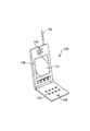
図29は、本発明に係る電子機器の一例である携帯電話機の一実施形態を示している。この携帯電話機100は、表示部としての液晶装置101と、アンテナ102と、スピーカ103と、キースイッチ群104と、マイクロホン105とを有する。
(Embodiment of electronic device)
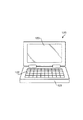
FIG. 29 shows an embodiment of a mobile phone which is an example of an electronic apparatus according to the invention. The
液晶装置101は、筐体としての外装ケースに収納されると共に、外装ケースの内部に設けた制御回路106によって制御されて、電話通信内容やインターネット情報等を表示する。この液晶装置101は、例えば、図3に示した液晶装置1を用いて構成できる。
The
図30は、本発明に係る電子機器の一例である腕時計の一実施形態を示している。この腕時計110は表示部として液晶装置111を有している。この液晶装置111は、筐体としての外装ケースに収納されると共に、外装ケースの内部に設けた制御回路112によって制御されて、時刻、日付等を情報として表示する。この液晶装置111は、例えば、図3に示した液晶装置1を用いて構成できる。
FIG. 30 shows an embodiment of a wrist watch that is an example of an electronic apparatus according to the invention. The
図31は、本発明に係る電子機器の一例である携帯型情報処理装置の一実施形態を示している。この携帯型情報処理装置120は、例えば、ワードプロセッサ、パーソナルコンピュータ等として提供されるものである。ここに示す携帯型情報処理装置120は、本体121の表面に設けられたキーボード等といった入力装置122と、表示部としての液晶装置123とを有する。本体121の内部に配設されたプロセッサの処理により、キーボード122を通して入力された情報や、その情報に基づく何等かの演算処理の結果が液晶装置123に表示される。
FIG. 31 shows an embodiment of a portable information processing apparatus which is an example of an electronic apparatus according to the invention. The portable
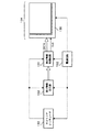
図32は、本発明に係る電子機器の他の実施形態を示している。ここに示す電子機器は、表示情報出力源130、表示情報処理回路131、電源回路132、タイミングジェネレータ133、液晶装置134、及び駆動回路136により構成される。
FIG. 32 shows another embodiment of the electronic apparatus according to the present invention. The electronic apparatus shown here includes a display
このうち、表示情報出力源130は、RAM(Random Access Memory)等といったメモリや、各種ディスク等といったストレージユニットや、ディジタル画像信号を同調出力する同調回路等を備え、タイミングジェネレータ133により生成される各種のクロック信号に基づいて、所定フォーマット画像信号等といった表示情報を表示情報処理回路131に供給する。
Among them, the display
次に、表示情報処理回路131は、増幅・反転回路や、ローテーション回路や、ガンマ補正回路や、クランプ回路等といった周知の回路を多数備え、入力した表示情報の処理を実行して、画像信号をクロック信号CLKと共に駆動回路136へ供給する。ここで、駆動回路136は、走査線駆動回路(図示せず)やデータ線駆動回路(図示せず)と共に、検査回路等を総称したものである。また、電源回路132は、上記の各構成要素に所定の電源電圧を供給する。
Next, the display
(その他の実施形態)
以上、好ましい実施形態を挙げて本発明を説明したが、本発明はその実施形態に限定されるものでなく、請求の範囲に記載した発明の範囲内で種々に改変できる。
(Other embodiments)
The present invention has been described with reference to the preferred embodiments. However, the present invention is not limited to the embodiments, and various modifications can be made within the scope of the invention described in the claims.
例えば、以上に説明した実施形態では反射パターンを構成する山部や谷部を規定する直交2軸を液晶装置1の基板の端辺が延在する方向XX及びYYに平行となるように設定したが、これに代えて、反射パターンに関する直交2軸方向と基板の端辺方向とに適宜の角度を持たせても良い。 For example, in the embodiment described above, the two orthogonal axes that define the crests and troughs constituting the reflection pattern are set to be parallel to the directions XX and YY in which the end sides of the substrate of the liquid crystal device 1 extend. However, instead of this, an appropriate angle may be given to the orthogonal two-axis direction with respect to the reflection pattern and the edge direction of the substrate.
また、図3に示した液晶装置1は単なる例示であり、本発明に係る液晶装置用基板を適用できる液晶装置は図3に示す構造以外の任意の液晶装置とすることができる。
(発明の効果)
3 is merely an example, and the liquid crystal device to which the substrate for a liquid crystal device according to the present invention can be applied can be any liquid crystal device other than the structure shown in FIG.
(The invention's effect)
本発明に係る液晶装置用基板、液晶装置及びそれらの製造方法並びに電子機器によれば、液晶装置の内部に入射した光を光反射膜によって反射させる際に、立体空間の全方位へ均一に反射するのではなく、特定の視野方向の光量又は強度が強くなるように反射できる。これにより、反射光が不要な視野角方向へ進行することを防止して、希望する視野角方向へ向かう反射光の光量を増大させることができ、これにより、希望の方向から見たときの表示の明るさを増大させることができる。 According to the liquid crystal device substrate, the liquid crystal device, the manufacturing method thereof, and the electronic apparatus according to the present invention, when the light incident on the liquid crystal device is reflected by the light reflecting film, it is uniformly reflected in all directions of the three-dimensional space. Instead, it can be reflected so that the amount of light or the intensity in a specific viewing direction is increased. As a result, it is possible to prevent the reflected light from traveling in an unnecessary viewing angle direction, and to increase the amount of reflected light toward the desired viewing angle direction, thereby displaying when viewed from the desired direction. Can increase the brightness.
1 液晶装置
2a,2b 基板
3 シール材
4a,4b 液晶駆動用IC
6a,6b 基板
7 TFT
8 有機絶縁膜
9 画素電極
10,10a,10b,10c,10d,10e 山部
13 電極
20,20a,20b,20c,20d,20e 谷部
28 マスク
29 マスクパターン
31 光反射膜
37 TFD
46 第1層
47 マスクパターン
48 マスク
49 第2層
51 マスク
52 反射膜
100 携帯電話機(電子機器)
110 腕時計(電子機器)
120 携帯型情報処理装置(電子機器)
L 液晶
S 光源
DESCRIPTION OF SYMBOLS 1
6a,
8
46
110 Watch (electronic equipment)
120 Portable information processing equipment (electronic equipment)
L Liquid crystal S Light source
Claims (13)
該光反射膜は光指向性及び光散乱性を呈するパターンを有し、
前記パターンは、尖った一端と緩やかに曲がる他端とを結んだ平面形状を有する液滴形状の複数の山部を並べて設けられてなり、
前記山部は、前記基材に直交する面であって、且つそれぞれが前記液滴形状の頂点に接するとともに、互いに直交する2つの面の断面形状が互いに異なることを特徴とする液晶装置用基板。 In a substrate for a liquid crystal device located on the opposite side to the observation side of the pair of substrates sandwiching the liquid crystal, and having a base material and a light reflecting film formed on the base material,
The light reflecting film has a pattern exhibiting light directivity and light scattering,
The pattern is provided by arranging a plurality of droplet-shaped crests having a planar shape connecting a sharp end and a gently curved other end,
The crest is a surface orthogonal to the base material, and is in contact with the apex of the droplet shape, and the cross-sectional shapes of two surfaces orthogonal to each other are different from each other. .
該光反射膜は光指向性及び光散乱性を呈するパターンを有し、
前記パターンは、尖った一端と緩やかに曲がる他端とを結んだ平面形状を有する液滴形状の複数の山部を並べて設けられてなり、
前記山部は、前記基材に直交する面であって、且つそれぞれが前記液滴形状の頂点に接するとともに、互いに直交する2つの面のうちの少なくとも一方の面によって区分される一方の側の立体形状と他方の側の立体形状とが互いに非対称であることを特徴とする液晶装置用基板。 In a substrate for a liquid crystal device located on the opposite side to the observation side of the pair of substrates sandwiching the liquid crystal, and having a base material and a light reflecting film formed on the base material,
The light reflecting film has a pattern exhibiting light directivity and light scattering,
The pattern is provided by arranging a plurality of droplet-shaped crests having a planar shape connecting a sharp end and a gently curved other end,
The crest is a surface orthogonal to the base material and is in contact with the apex of the droplet shape and is separated by at least one of the two surfaces orthogonal to each other. A substrate for a liquid crystal device, wherein the three-dimensional shape and the three-dimensional shape on the other side are asymmetric with each other.
該光反射膜には、尖った一端と緩やかに曲がる他端とを結んだ平面形状を有する液滴形状の複数の山部を並べて成る光反射パターンが形成され、
該光反射パターンで反射する光の光量に関して、前記基材に直交する面であって、且つそれぞれが前記液滴形状の頂点に接するとともに、互いに直交する2つの面において、法線方向から入射した光の前記2つの面のうちの一方の面に沿った反射光量の変化と、前記2つの面のうちの他方の面に沿った反射光量の変化とが互いに異なることを特徴とする液晶装置用基板。 In a substrate for a liquid crystal device located on the opposite side to the observation side of the pair of substrates sandwiching the liquid crystal, and having a base material and a light reflecting film formed on the base material,
The light reflecting film is formed with a light reflecting pattern in which a plurality of droplet-shaped crests having a planar shape connecting a sharp end and a gently bent other end are arranged,
With respect to the amount of light reflected by the light reflection pattern, the light is incident from the normal direction on two surfaces that are orthogonal to the substrate and that are in contact with the top of the droplet shape and orthogonal to each other. For a liquid crystal device, the change in the amount of reflected light along one of the two surfaces is different from the change in the amount of reflected light along the other of the two surfaces substrate.
該光反射膜は光指向性及び光散乱性を呈するパターンを有し、
前記パターンは液滴形状の複数の谷部を並べて設けられてなり、
前記谷部は、前記基材に直交する面であって、且つそれぞれが前記液滴形状の最深部に接するとともに、互いに直交する2つの面の断面形状が互いに異なることを特徴とする液晶装置用基板。 In a substrate for a liquid crystal device located on the opposite side to the observation side of the pair of substrates sandwiching the liquid crystal, and having a base material and a light reflecting film formed on the base material,
The light reflecting film has a pattern exhibiting light directivity and light scattering,
The pattern is formed by arranging a plurality of droplet-shaped valleys,
The valley portion is a surface orthogonal to the base material, and is in contact with the deepest portion of the droplet shape, and the cross-sectional shapes of two surfaces orthogonal to each other are different from each other. substrate.
基材と、該基材上に形成された光反射膜とを有し、
該光反射膜は光指向性及び光散乱性を呈するパターンを有し、
前記パターンは液滴形状の複数の谷部を並べて設けられてなり、
前記谷部は、前記基材に直交する面であって、且つそれぞれが前記液滴形状の最深部に接するとともに、互いに直交する2つの面のうちの少なくとも一方の面によって区分される一方の側の立体形状と他方の側の立体形状とが互いに非対称であることを特徴とする液晶装置用基板。 In the substrate for the liquid crystal device located on the opposite side to the observation side among the pair of substrates sandwiching the liquid crystal,
A base material, and a light reflecting film formed on the base material,
The light reflecting film has a pattern exhibiting light directivity and light scattering,
The pattern is formed by arranging a plurality of droplet-shaped valleys,
The valley portion is a surface orthogonal to the base material and is in contact with the deepest portion of the droplet shape and is separated by at least one surface of two surfaces orthogonal to each other A substrate for a liquid crystal device, wherein the three-dimensional shape and the three-dimensional shape on the other side are asymmetric with each other.
該光反射膜には液滴形状の複数の谷部を並べて成る光反射パターンが形成され、
該光反射パターンで反射する光の光量に関して、前記基材に直交する面であって、且つそれぞれが前記液滴形状の最深部に接するとともに、互いに直交する2つの面において、法線方向から入射した光の前記2つの面のうちの一方の面に沿った反射光量の変化と、前記2つの面のうちの他方の面に沿った反射光量の変化とが互いに異なることを特徴とする液晶装置用基板。 In a substrate for a liquid crystal device located on the opposite side to the observation side of the pair of substrates sandwiching the liquid crystal, and having a base material and a light reflecting film formed on the base material,
The light reflecting film is formed with a light reflecting pattern in which a plurality of droplet-shaped valleys are arranged,
With respect to the amount of light reflected by the light reflection pattern, the light is incident on the two surfaces perpendicular to the base material and in contact with the deepest part of the droplet shape from the normal direction. A change in the amount of reflected light along one of the two surfaces of the light and a change in the amount of reflected light along the other of the two surfaces are different from each other. Substrate.
An electronic apparatus having a liquid crystal device for displaying an image, a housing for housing the liquid crystal device, and a control circuit for controlling the liquid crystal device, wherein the liquid crystal device is configured by the liquid crystal device according to claim 12. An electronic device characterized by that.
Priority Applications (1)
| Application Number | Priority Date | Filing Date | Title |
|---|---|---|---|
| JP2005156732A JP4155282B2 (en) | 2000-12-25 | 2005-05-30 | Substrate for liquid crystal device, liquid crystal device and electronic apparatus |
Applications Claiming Priority (2)
| Application Number | Priority Date | Filing Date | Title |
|---|---|---|---|
| JP2000392828 | 2000-12-25 | ||
| JP2005156732A JP4155282B2 (en) | 2000-12-25 | 2005-05-30 | Substrate for liquid crystal device, liquid crystal device and electronic apparatus |
Related Parent Applications (1)
| Application Number | Title | Priority Date | Filing Date |
|---|---|---|---|
| JP2001347606A Division JP3711913B2 (en) | 2000-12-25 | 2001-11-13 | Substrate for liquid crystal device, liquid crystal device and electronic apparatus |
Publications (2)
| Publication Number | Publication Date |
|---|---|
| JP2005292851A true JP2005292851A (en) | 2005-10-20 |
| JP4155282B2 JP4155282B2 (en) | 2008-09-24 |
Family
ID=35325762
Family Applications (1)
| Application Number | Title | Priority Date | Filing Date |
|---|---|---|---|
| JP2005156732A Expired - Lifetime JP4155282B2 (en) | 2000-12-25 | 2005-05-30 | Substrate for liquid crystal device, liquid crystal device and electronic apparatus |
Country Status (1)
| Country | Link |
|---|---|
| JP (1) | JP4155282B2 (en) |
-
2005
- 2005-05-30 JP JP2005156732A patent/JP4155282B2/en not_active Expired - Lifetime
Also Published As
| Publication number | Publication date |
|---|---|
| JP4155282B2 (en) | 2008-09-24 |
Similar Documents
| Publication | Publication Date | Title |
|---|---|---|
| JP4223094B2 (en) | Electro-optic display | |
| US7352420B2 (en) | Liquid crystal display and electronic appliance | |
| KR100416173B1 (en) | Display device substrate, method for manufacturing the display device substrate, liquid-crystal display device, and electronic equipment | |
| KR100332519B1 (en) | Liquid crystal display device | |
| TW594220B (en) | Liquid crystal display device | |
| JP2000002872A (en) | Liquid crystal display device and its manufacture | |
| JP3711913B2 (en) | Substrate for liquid crystal device, liquid crystal device and electronic apparatus | |
| JP2007212969A (en) | REFLECTOR, LIQUID CRYSTAL DISPLAY DEVICE PROVIDED WITH THE REFLECTOR AND MANUFACTURING METHOD THEREOF | |
| JP2008145525A (en) | Liquid crystal device and electronic device | |
| JP2009139853A (en) | Liquid crystal display device | |
| KR20050068872A (en) | Device and fabrication method for liquid crystal display of transflective type | |
| KR100979385B1 (en) | Semi-transmissive liquid crystal display device and manufacturing method thereof | |
| CN101059612B (en) | Method for manufacturing semi-transmissive and semi-reflective liquid crystal panel and active element array substrate | |
| JP4001009B2 (en) | Liquid crystal display device and electronic device | |
| JP3888329B2 (en) | Substrate for liquid crystal device, method for manufacturing substrate for liquid crystal device, liquid crystal device, method for manufacturing liquid crystal device, and electronic apparatus | |
| JP4155282B2 (en) | Substrate for liquid crystal device, liquid crystal device and electronic apparatus | |
| JP3931599B2 (en) | Reflector manufacturing method and liquid crystal display device manufacturing method | |
| JP5121488B2 (en) | Liquid crystal device and electronic device | |
| KR101006798B1 (en) | Semi-transmissive liquid crystal display device and manufacturing method thereof | |
| KR101000442B1 (en) | Reflective-transmissive polysilicon liquid crystal display and manufacturing method thereof | |
| JP4511248B2 (en) | Liquid crystal display | |
| JP2001305996A (en) | Display device substrate and method of manufacturing the same, liquid crystal device and electronic apparatus | |
| JP2004004938A (en) | Liquid crystal display and electronic equipment | |
| JP3575764B2 (en) | Manufacturing method of liquid crystal display device | |
| JP2008107524A (en) | Electro-optical device and manufacturing method thereof |
Legal Events
| Date | Code | Title | Description |
|---|---|---|---|
| RD04 | Notification of resignation of power of attorney |
Free format text: JAPANESE INTERMEDIATE CODE: A7424 Effective date: 20070403 |
|
| A977 | Report on retrieval |
Free format text: JAPANESE INTERMEDIATE CODE: A971007 Effective date: 20080104 |
|
| A131 | Notification of reasons for refusal |
Free format text: JAPANESE INTERMEDIATE CODE: A131 Effective date: 20080115 |
|
| A521 | Written amendment |
Free format text: JAPANESE INTERMEDIATE CODE: A523 Effective date: 20080307 |
|
| TRDD | Decision of grant or rejection written | ||
| A01 | Written decision to grant a patent or to grant a registration (utility model) |
Free format text: JAPANESE INTERMEDIATE CODE: A01 Effective date: 20080617 |
|
| A01 | Written decision to grant a patent or to grant a registration (utility model) |
Free format text: JAPANESE INTERMEDIATE CODE: A01 |
|
| A61 | First payment of annual fees (during grant procedure) |
Free format text: JAPANESE INTERMEDIATE CODE: A61 Effective date: 20080630 |
|
| FPAY | Renewal fee payment (event date is renewal date of database) |
Free format text: PAYMENT UNTIL: 20110718 Year of fee payment: 3 |
|
| R150 | Certificate of patent or registration of utility model |
Free format text: JAPANESE INTERMEDIATE CODE: R150 Ref document number: 4155282 Country of ref document: JP Free format text: JAPANESE INTERMEDIATE CODE: R150 |
|
| FPAY | Renewal fee payment (event date is renewal date of database) |
Free format text: PAYMENT UNTIL: 20110718 Year of fee payment: 3 |
|
| FPAY | Renewal fee payment (event date is renewal date of database) |
Free format text: PAYMENT UNTIL: 20120718 Year of fee payment: 4 |
|
| FPAY | Renewal fee payment (event date is renewal date of database) |
Free format text: PAYMENT UNTIL: 20120718 Year of fee payment: 4 |
|
| FPAY | Renewal fee payment (event date is renewal date of database) |
Free format text: PAYMENT UNTIL: 20130718 Year of fee payment: 5 |
|
| R250 | Receipt of annual fees |
Free format text: JAPANESE INTERMEDIATE CODE: R250 |
|
| S111 | Request for change of ownership or part of ownership |
Free format text: JAPANESE INTERMEDIATE CODE: R313113 |
|
| S111 | Request for change of ownership or part of ownership |
Free format text: JAPANESE INTERMEDIATE CODE: R313113 |
|
| R371 | Transfer withdrawn |
Free format text: JAPANESE INTERMEDIATE CODE: R371 |
|
| S111 | Request for change of ownership or part of ownership |
Free format text: JAPANESE INTERMEDIATE CODE: R313113 |
|
| R350 | Written notification of registration of transfer |
Free format text: JAPANESE INTERMEDIATE CODE: R350 |
|
| R250 | Receipt of annual fees |
Free format text: JAPANESE INTERMEDIATE CODE: R250 |
|
| R250 | Receipt of annual fees |
Free format text: JAPANESE INTERMEDIATE CODE: R250 |
|
| R250 | Receipt of annual fees |
Free format text: JAPANESE INTERMEDIATE CODE: R250 |
|
| R250 | Receipt of annual fees |
Free format text: JAPANESE INTERMEDIATE CODE: R250 |
|
| R250 | Receipt of annual fees |
Free format text: JAPANESE INTERMEDIATE CODE: R250 |
|
| R250 | Receipt of annual fees |
Free format text: JAPANESE INTERMEDIATE CODE: R250 |
|
| EXPY | Cancellation because of completion of term |