JP2005292566A - Electro-optical device and electronic apparatus - Google Patents
Electro-optical device and electronic apparatus Download PDFInfo
- Publication number
- JP2005292566A JP2005292566A JP2004109084A JP2004109084A JP2005292566A JP 2005292566 A JP2005292566 A JP 2005292566A JP 2004109084 A JP2004109084 A JP 2004109084A JP 2004109084 A JP2004109084 A JP 2004109084A JP 2005292566 A JP2005292566 A JP 2005292566A
- Authority
- JP
- Japan
- Prior art keywords
- circuit chip
- electro
- pixels
- basic
- optical device
- Prior art date
- Legal status (The legal status is an assumption and is not a legal conclusion. Google has not performed a legal analysis and makes no representation as to the accuracy of the status listed.)
- Pending
Links
Images


Landscapes
- Devices For Indicating Variable Information By Combining Individual Elements (AREA)
- Electroluminescent Light Sources (AREA)
Abstract
【課題】 電気光学装置の製造コストの削減を可能とする技術を提供すること。
【解決手段】 複数の色画素を含んでなる基本画素をマトリクス状に複数配列した表示領域を備え、当該表示領域が線順次走査方式で駆動される電気光学装置であって、複数の色画素を構成する複数の電気光学素子と、複数の基本画素のうち垂直走査方向に隣接配置される2つの基本画素ごとに1つ設けられて当該2つの基本画素を制御するための回路チップ(16)と、複数の配線(走査線51,524、データ線41R等、電源線53R等)と、これら配線と回路チップとの相互間に設けられる複数の接続端子(63)と、を含み、回路チップとデータ線との電気的接続を担う接続端子が、回路チップ内の各駆動回路のうちで隣接配置される2つの基本画素内の同色の色画素のそれぞれに対応する2つの駆動回路ごとに共用されて設けられているものである。
【選択図】 図2
PROBLEM TO BE SOLVED: To provide a technique capable of reducing the manufacturing cost of an electro-optical device.
An electro-optical device includes a display area in which a plurality of basic pixels including a plurality of color pixels are arranged in a matrix, and the display area is driven by a line-sequential scanning method. A plurality of electro-optic elements to be configured, and a circuit chip (16) for controlling two basic pixels, one provided for each of two basic pixels arranged adjacent to each other in the vertical scanning direction among the plurality of basic pixels A plurality of wirings (scanning lines 51, 524, data lines 41R, etc., power supply lines 53R, etc.) and a plurality of connection terminals (63) provided between these wirings and the circuit chip. Are connected to each of the two drive circuits corresponding to each of the same color pixels in the two basic pixels arranged adjacent to each other among the drive circuits in the circuit chip. It is what has been.
[Selection] Figure 2
Description
本発明は、薄膜トランジスタ等の素子を用いて画素駆動を行う表示装置(電気光学装置)及びその製造方法に関する。 The present invention relates to a display device (electro-optical device) that performs pixel driving using an element such as a thin film transistor and a method for manufacturing the same.
薄膜トランジスタを画素駆動に用いる表示装置(電気光学装置)、例えば、薄膜トランジスタ駆動液晶表示装置、薄膜トランジスタ駆動有機エレクトロルミネッセンス表示装置、薄膜トランジスタ駆動発光ダイオード表示装置、薄膜トランジスタ駆動電気泳動表示装置などでは、薄膜トランジスタは装置全体の一部分をなすものであり、それ以外の大部分は配線や支持基板などからなる場合が少なくない。このような表示装置(薄膜トランジスタ駆動表示装置)を、薄膜トランジスタと配線や支持基板を一体として同一の製造プロセスを経て製造する場合には、薄膜トランジスタを作成するための高度で複雑な製造プロセスが必要とされるため、一般的に、製造コストが高額になる。しかしながら、配線や支持基板だけのためには、高度で複雑な製造プロセスは必要とされず、製造コストは安価である。もし、薄膜トランジスタと配線や支持基板を別個に作成し、必要とされる部分にだけ薄膜トランジスタを配置することができれば、薄膜トランジスタ駆動表示装置の製造コストを低減することが可能である。 In a display device (electro-optical device) using a thin film transistor for pixel driving, for example, a thin film transistor driving liquid crystal display device, a thin film transistor driving organic electroluminescence display device, a thin film transistor driving light emitting diode display device, a thin film transistor driving electrophoretic display device, etc. Most of the other parts are often made of wiring or a supporting substrate. When such a display device (thin film transistor drive display device) is manufactured through the same manufacturing process by integrating the thin film transistor, the wiring, and the support substrate, a sophisticated and complicated manufacturing process for forming the thin film transistor is required. Therefore, in general, the manufacturing cost becomes high. However, an advanced and complicated manufacturing process is not required only for the wiring and the supporting substrate, and the manufacturing cost is low. If the thin film transistor, the wiring, and the support substrate are separately formed and the thin film transistor can be disposed only in a necessary portion, the manufacturing cost of the thin film transistor drive display device can be reduced.
このような要望に対して、転写元基材上に剥離層を介して、薄膜トランジスタ等の素子からなる被転写層を形成し、これを総て転写先基材に接合してから剥離層に光を照射し剥離を生じさせ、転写元基材を剥離層から離脱させることにより、転写先基材上の所望の位置に素子を形成する転写方法が開発されている。このような転写方法は、例えば、特開平10−125931号公報に開示されている(特許文献1)。上述した転写方法を用いることにより、必要とされる部分にだけ薄膜トランジスタを配置することができるので、全体として平均すれば、この薄膜トランジスタ駆動表示装置の製造コストを低減することが可能となる。 In response to such a demand, a transfer layer composed of an element such as a thin film transistor is formed on the transfer source substrate via a release layer, and all of the layers are bonded to the transfer destination substrate, and then light is applied to the release layer. A transfer method has been developed in which an element is formed at a desired position on a transfer destination base material by irradiating the film to cause peeling and separating the transfer source base material from the release layer. Such a transfer method is disclosed, for example, in JP-A-10-125931 (Patent Document 1). By using the transfer method described above, thin film transistors can be arranged only in necessary portions. Therefore, if averaged as a whole, the manufacturing cost of the thin film transistor drive display device can be reduced.
上述した転写方法を用いて電気光学装置(表示装置)を製造する場合に、被転写体と転写先基材との相互間に接続端子(電極パッド)を介在させて両者間を電気的に接続するフリップチップ接続を採用することが検討されている。現状では、接続信頼性を確保するために、比較的大きな接続端子を設ける必要がある。このため、回路チップ全体の面積は、集積される電気回路の占める面積よりも接続端子を配置するための面積が支配的である。このような理由により回路チップの面積の削減が難しいことから、単位面積当たりに形成可能な回路チップの数が少なくなり、1チップ当たりのコストの削減が難しかった。また、表示装置は通常、多数の画素を有することから、これらの画素のそれぞれに上記転写技術などを用いて薄膜回路を形成する場合には、回路チップの実装回数が非常に多くなり製造コストの削減の妨げとなる。 When an electro-optical device (display device) is manufactured using the transfer method described above, a connection terminal (electrode pad) is interposed between the transfer target and the transfer destination base material to electrically connect the two. It has been considered to employ flip chip connection. At present, it is necessary to provide relatively large connection terminals in order to ensure connection reliability. For this reason, the area for arranging the connection terminals is more dominant than the area occupied by the integrated electric circuit. For this reason, it is difficult to reduce the area of the circuit chip. Therefore, the number of circuit chips that can be formed per unit area is reduced, and it is difficult to reduce the cost per chip. In addition, since a display device usually has a large number of pixels, when a thin film circuit is formed on each of these pixels by using the transfer technique or the like, the number of circuit chip mountings is very large, resulting in a low manufacturing cost. This hinders reduction.
そこで、本発明は、有機EL表示装置等の電気光学装置の製造コストの削減を可能とする技術を提供することを目的とする。 SUMMARY An advantage of some aspects of the invention is that it provides a technique capable of reducing the manufacturing cost of an electro-optical device such as an organic EL display device.
第1の態様の本発明は、複数の色画素を含んでなる基本画素をマトリクス状に複数配列した表示領域を備え、当該表示領域が線順次走査方式で駆動される電気光学装置であって、複数の上記色画素を構成する複数の電気光学素子と、複数の上記基本画素のうち、垂直走査方向に隣接配置される2つの基本画素ごとに1つ設けられ、当該2つの基本画素に含まれる各色画素に対応する電気光学素子のそれぞれを制御するための複数の駆動回路を含む回路チップと、上記電気光学素子の駆動に用いる走査信号を上記回路チップに供給するための複数の走査線と、上記電気光学素子の駆動に用いるデータ信号を上記回路チップに供給するための複数のデータ線と、上記電気光学素子を発光させるための電力を上記回路チップに供給するための複数の電源線と、上記回路チップと、上記走査線、上記データ線及び上記電源線との相互間に設けられて電気的接続を担う複数の接続端子と、を含み、上記回路チップと上記データ線との電気的接続を担う上記接続端子は、上記回路チップ内の各駆動回路のうちで上記隣接配置される2つの基本画素内の同色の色画素のそれぞれに対応する2つの駆動回路ごとに共用されて設けられている電気光学装置である。 The first aspect of the present invention is an electro-optical device that includes a display region in which a plurality of basic pixels including a plurality of color pixels are arranged in a matrix, and the display region is driven by a line-sequential scanning method. Among the plurality of electro-optic elements constituting the plurality of color pixels and the plurality of basic pixels, one is provided for every two basic pixels arranged adjacent to each other in the vertical scanning direction, and is included in the two basic pixels. A circuit chip including a plurality of drive circuits for controlling each of the electro-optic elements corresponding to each color pixel; a plurality of scan lines for supplying a scan signal used for driving the electro-optic elements to the circuit chip; A plurality of data lines for supplying data signals used for driving the electro-optical element to the circuit chip, and a plurality of data lines for supplying power for causing the electro-optical element to emit light to the circuit chip. Including a source line, the circuit chip, and a plurality of connection terminals provided between the scanning line, the data line, and the power supply line for electrical connection, and the circuit chip and the data line. The connection terminal responsible for the electrical connection is shared by two drive circuits corresponding to the same color pixels in the two adjacently arranged basic pixels among the drive circuits in the circuit chip. The electro-optical device is provided.
隣接する2画素に着目し、これらに含まれる各電気光学素子のそれぞれに対する駆動回路(画素駆動回路)を1つの回路チップに集約することにより、転写技術やその他の実装技術を用いて回路チップを形成する際の実装回数(転写回数)が削減される。また、駆動回路の集約に伴い、回路チップに含まれる画素駆動回路のうち共通化が可能なものについては適宜共通配線とすることにより、当該回路チップと外部との電気的接続を担う電極パッドの数を削減してチップ面積の縮小を図ることができる。これらにより、単位面積当たりに製造可能なチップ数が増加し、かつチップの実装回数が削減されるので、有機EL表示装置等の電気光学装置の製造コストを削減することが可能となる。 Focusing on two adjacent pixels, and consolidating the drive circuits (pixel drive circuits) for each of the electro-optical elements included in these into one circuit chip, the circuit chip is transferred using transfer technology or other mounting technology. The number of mountings (transfer times) during formation is reduced. In addition, with the consolidation of the drive circuits, the pixel drive circuits included in the circuit chip that can be shared are appropriately set as a common wiring so that the electrode pads that are responsible for the electrical connection between the circuit chip and the outside are appropriately used. The chip area can be reduced by reducing the number. As a result, the number of chips that can be manufactured per unit area is increased and the number of chip mountings is reduced, so that the manufacturing cost of an electro-optical device such as an organic EL display device can be reduced.
また、上記回路チップと上記電源線との電気的接続を担う上記接続端子は、上記回路チップ内の各駆動回路のうちで、隣接配置される上記2つの基本画素内の同色の色画素のそれぞれに対応する2つの駆動回路ごとに共用されて設けられていることが好ましい。 Further, the connection terminal responsible for electrical connection between the circuit chip and the power line is each of the same color pixels in the two basic pixels arranged adjacent to each other among the drive circuits in the circuit chip. It is preferable that each of the two drive circuits corresponding to is provided in common.
これにより、接続端子の数を更に削減し、チップ面積の縮小化を図ることが可能となる。 As a result, the number of connection terminals can be further reduced, and the chip area can be reduced.
また、上記回路チップと上記走査線との電気的接続を担う上記接続端子は、上記回路チップ内の各駆動回路のうちで上記基本画素のそれぞれに対応する3つの駆動回路ごとに共用されて設けられていることが好ましい。 In addition, the connection terminal responsible for electrical connection between the circuit chip and the scanning line is provided for each of the three drive circuits corresponding to the basic pixels among the drive circuits in the circuit chip. It is preferable that
これにより、接続端子の数を更に削減し、チップ面積の縮小化を図ることが可能となる。 As a result, the number of connection terminals can be further reduced, and the chip area can be reduced.
また、上記回路チップは、隣接配置される上記2つの基本画素の境界付近に配置されることが好ましい。 The circuit chip is preferably arranged in the vicinity of a boundary between the two basic pixels arranged adjacent to each other.
これにより、各基本画素と回路チップとの距離がほぼ均等になり、両者間を接続する補助配線の引き回しなどのレイアウト設計が容易となる。 As a result, the distance between each basic pixel and the circuit chip becomes almost equal, and layout design such as routing of auxiliary wiring connecting the two becomes easy.
また、上記回路チップ内の各駆動回路は、上記電気光学素子に流れる電流を制御する第1のトランジスタと、当該第1のトランジスタを上記データ信号に応じて動作させる第2のトランジスタと、を含んで構成されることが好ましい。 Each drive circuit in the circuit chip includes a first transistor that controls a current flowing through the electro-optic element, and a second transistor that operates the first transistor in accordance with the data signal. It is preferable that it is comprised.
また、上記電気光学素子が有機エレクトロルミネセンス(EL)素子であることが好ましい。 The electro-optical element is preferably an organic electroluminescence (EL) element.
これにより、低コストな有機EL表示装置が得られる。 Thereby, a low-cost organic EL display device is obtained.
第2の態様の本発明は、複数の色画素を含んでなる基本画素をマトリクス状に複数配列した表示領域を備え、当該表示領域が線順次走査方式で駆動される電気光学装置であって、複数の上記色画素を構成する複数の電気光学素子と、複数の上記基本画素のうち、走査タイミングが同じであり、かつ相互に隣接配置される2つの基本画素ごとに1つ設けられ、当該2つの基本画素に含まれる各色画素に対応する電気光学素子のそれぞれを制御するための複数の駆動回路を含む回路チップと、上記電気光学素子の駆動に用いる走査信号を上記回路チップに供給するための複数の走査線と、上記電気光学素子の駆動に用いるデータ信号を上記回路チップに供給するための複数のデータ線と、上記電気光学素子を発光させるための電力を上記回路チップに供給するための複数の電源線と、上記回路チップと、上記走査線、上記データ線及び上記電源線との相互間に設けられて電気的接続を担う複数の接続端子と、を含み、上記回路チップと上記走査線との電気的接続を担う上記接続端子は、上記回路チップ内の各駆動回路に共用されて設けられている電気光学装置である。 The second aspect of the present invention is an electro-optical device that includes a display region in which a plurality of basic pixels including a plurality of color pixels are arranged in a matrix, and the display region is driven by a line-sequential scanning method. Among the plurality of electro-optical elements constituting the plurality of color pixels and the plurality of basic pixels, one is provided for each of two basic pixels having the same scanning timing and arranged adjacent to each other. A circuit chip including a plurality of drive circuits for controlling each of the electro-optical elements corresponding to each color pixel included in one basic pixel, and a scanning signal used to drive the electro-optical elements A plurality of scanning lines, a plurality of data lines for supplying a data signal used for driving the electro-optical element to the circuit chip, and a power for causing the electro-optical element to emit light are supplied to the circuit chip. Including a plurality of power supply lines for supplying to the circuit chip, a plurality of connection terminals provided between the scanning lines, the data lines, and the power supply lines for electrical connection. The connection terminal responsible for electrical connection between the circuit chip and the scanning line is an electro-optical device provided to be shared by each drive circuit in the circuit chip.
隣接する2画素に着目し、これらに含まれる各電気光学素子のそれぞれに対する駆動回路(画素駆動回路)を1つの回路チップに集約することにより、転写技術やその他の実装技術を用いて回路チップを形成する際の実装回数(転写回数)を削減している。また、駆動回路の集約に伴い、回路チップに含まれる画素駆動回路のうち共通化が可能なものについては適宜共通配線とすることにより、当該回路チップと外部との電気的接続を担う電極パッドの数を削減し、チップ面積の縮小を図ることができる。これらにより、単位面積当たりに製造可能なチップ数が増加し、かつチップの実装回数が削減されるので、有機EL表示装置等の電気光学装置の製造コストを削減することが可能となる。 Focusing on two adjacent pixels, and consolidating the drive circuits (pixel drive circuits) for each of the electro-optical elements included in these into one circuit chip, the circuit chip is transferred using transfer technology or other mounting technology. The number of times of mounting (number of times of transfer) when forming is reduced. In addition, with the consolidation of the drive circuits, the pixel drive circuits included in the circuit chip that can be shared are appropriately set as a common wiring so that the electrode pads that are responsible for the electrical connection between the circuit chip and the outside are appropriately used. The number can be reduced and the chip area can be reduced. As a result, the number of chips that can be manufactured per unit area is increased and the number of chip mountings is reduced, so that the manufacturing cost of an electro-optical device such as an organic EL display device can be reduced.
また、上記回路チップと上記電源線との電気的接続を担う上記接続端子は、上記回路チップ内の各駆動回路のうちで上記隣接配置される2つの基本画素内の同色の色画素のそれぞれに対応する2つの駆動回路ごとに共用されて設けられていることが好ましい。 Further, the connection terminal responsible for electrical connection between the circuit chip and the power supply line is connected to each of the same color pixels in the two basic pixels arranged adjacent to each other among the drive circuits in the circuit chip. It is preferable that the two corresponding driving circuits are provided in common.
これにより、接続端子の数を更に削減し、チップ面積の縮小化を図ることが可能となる。 As a result, the number of connection terminals can be further reduced, and the chip area can be reduced.
また、上記回路チップは、隣接配置される上記2つの基本画素の境界付近に配置されることが好ましい。 The circuit chip is preferably arranged in the vicinity of a boundary between the two basic pixels arranged adjacent to each other.
これにより、各基本画素と回路チップとの距離がほぼ均等になり、両者間を接続する補助配線の引き回しなどのレイアウト設計が容易となる。 As a result, the distance between each basic pixel and the circuit chip becomes almost equal, and layout design such as routing of auxiliary wiring connecting the two becomes easy.
また、上記回路チップ内の各駆動回路は、上記電気光学素子に流れる電流を制御する第1のトランジスタと、当該第1のトランジスタを上記データ信号に応じて動作させる第2のトランジスタと、を含んで構成されることが好ましい。 Each drive circuit in the circuit chip includes a first transistor that controls a current flowing through the electro-optic element, and a second transistor that operates the first transistor in accordance with the data signal. It is preferable that it is comprised.
また、上記電気光学素子が有機エレクトロルミネセンス(EL)素子であることが好ましい。 The electro-optical element is preferably an organic electroluminescence (EL) element.
これにより、低コストな有機EL表示装置が得られる。 Thereby, a low-cost organic EL display device is obtained.
第3の態様の本発明は、複数の色画素を含んでなる基本画素をマトリクス状に複数配列した表示領域を備え、当該表示領域が線順次走査方式で駆動される電気光学装置であって、複数の上記色画素を構成する複数の電気光学素子と、複数の上記基本画素のうち、走査タイミングが同じであり隣接配置される2つの基本画素と、当該2つの基本画素のそれぞれと垂直走査方向に隣接配置される2つの基本画素とを合わせた4つの基本画素ごとに1つ設けられ、当該4つの基本画素に含まれる各色画素に対応する電気光学素子のそれぞれを制御するための複数の駆動回路を含む回路チップと、上記電気光学素子の駆動に用いる走査信号を上記回路チップに供給するための複数の走査線と、上記電気光学素子の駆動に用いるデータ信号を上記回路チップに供給するための複数のデータ線と、上記電気光学素子を発光させるための電力を上記回路チップに供給するための複数の電源線と、上記回路チップと、上記走査線、上記データ線及び上記電源線との相互間に設けられて電気的接続を担う複数の接続端子と、を含み、上記回路チップと上記走査線との電気的接続を担う上記接続端子は、上記回路チップ内の各駆動回路のうちで、上記走査タイミングが同じであり隣接配置される2つの基本画素内の各駆動回路に共用されて設けられ、上記回路チップと上記データ線との電気的接続を担う上記接続端子は、上記回路チップ内の各駆動回路のうちで上記垂直走査方向に隣接配置される2つの基本画素内の同色の色画素のそれぞれに対応する2つの駆動回路ごとに共用されて設けられている電気光学装置である。 The third aspect of the present invention is an electro-optical device that includes a display region in which a plurality of basic pixels including a plurality of color pixels are arranged in a matrix, and the display region is driven by a line-sequential scanning method. The plurality of electro-optic elements constituting the plurality of color pixels, the two basic pixels having the same scanning timing among the plurality of basic pixels, and the vertical scanning direction of each of the two basic pixels A plurality of drives for controlling each of the electro-optic elements corresponding to the color pixels included in the four basic pixels, provided for each of the four basic pixels including two basic pixels arranged adjacent to each other A circuit chip including a circuit, a plurality of scanning lines for supplying a scanning signal used for driving the electro-optical element to the circuit chip, and a data signal used for driving the electro-optical element. A plurality of data lines for supplying the circuit chip, a plurality of power lines for supplying power for causing the electro-optic element to emit light to the circuit chip, the circuit chip, the scanning line, the data line, and A plurality of connection terminals provided between the power supply lines and responsible for electrical connection, and the connection terminals responsible for electrical connection between the circuit chip and the scanning line are each included in the circuit chip. Among the drive circuits, the connection terminals that share the same scanning timing and are shared by the drive circuits in two adjacent basic pixels and are responsible for electrical connection between the circuit chip and the data line Is shared by two drive circuits corresponding to each of the same color pixels in the two basic pixels arranged adjacent to each other in the vertical scanning direction among the drive circuits in the circuit chip. Electric It is an optical device.
隣接する4画素に着目し、これらに含まれる各電気光学素子のそれぞれに対する駆動回路(画素駆動回路)を1つの回路チップに集約することにより、転写技術やその他の実装技術を用いて回路チップを形成する際の実装回数(転写回数)が削減される。また、駆動回路の集約に伴い、回路チップに含まれる画素駆動回路のうち共通化が可能なものについては適宜共通配線とすることにより、当該回路チップと外部との電気的接続を担う電極パッドの数を削減し、チップ面積の縮小を図ることができる。これらにより、単位面積当たりに製造可能なチップ数が増加し、かつチップの実装回数が削減されるので、有機EL表示装置等の電気光学装置の製造コストを削減することが可能となる。 Focusing on the adjacent four pixels, the drive circuit (pixel drive circuit) for each of the electro-optic elements included in these pixels is integrated into one circuit chip, so that the circuit chip is transferred using transfer technology or other mounting technology. The number of mountings (transfer times) during formation is reduced. In addition, with the consolidation of the drive circuits, the pixel drive circuits included in the circuit chip that can be shared are appropriately set as a common wiring so that the electrode pads that are responsible for the electrical connection between the circuit chip and the outside are appropriately used. The number can be reduced and the chip area can be reduced. As a result, the number of chips that can be manufactured per unit area is increased and the number of chip mountings is reduced, so that the manufacturing cost of an electro-optical device such as an organic EL display device can be reduced.
また、上記回路チップと上記電源線との電気的接続を担う上記接続端子は、上記回路チップ内の各駆動回路のうちで上記基本画素内の同色の色画素のそれぞれに対応する4つの駆動回路ごとに共用されて設けられていることが好ましい。 The connection terminals responsible for electrical connection between the circuit chip and the power line are four drive circuits corresponding to the same color pixels in the basic pixel among the drive circuits in the circuit chip. It is preferable that each is provided in common.
これにより、接続端子の数を更に削減し、チップ面積の縮小化を図ることが可能となる。 As a result, the number of connection terminals can be further reduced, and the chip area can be reduced.
また、上記回路チップは、隣接配置される上記4つの基本画素の相互の境界付近に配置されることが好ましい。 The circuit chip is preferably arranged in the vicinity of the boundary between the four basic pixels arranged adjacent to each other.
これにより、各基本画素と回路チップとの距離がほぼ均等になり、両者間を接続する補助配線の引き回しなどのレイアウト設計が容易となる。 As a result, the distance between each basic pixel and the circuit chip becomes almost equal, and layout design such as routing of auxiliary wiring connecting the two becomes easy.
また、上記回路チップ内の各駆動回路は、上記電気光学素子に流れる電流を制御する第1のトランジスタと、当該第1のトランジスタを上記データ信号に応じて動作させる第2のトランジスタと、を含んで構成されることが好ましい。 Each drive circuit in the circuit chip includes a first transistor that controls a current flowing through the electro-optic element, and a second transistor that operates the first transistor in accordance with the data signal. It is preferable that it is comprised.
また、上記電気光学素子が有機エレクトロルミネセンス(EL)素子であることが好ましい。 The electro-optical element is preferably an organic electroluminescence (EL) element.
これにより、低コストな有機EL表示装置が得られる。 Thereby, a low-cost organic EL display device is obtained.
第4の態様の本発明は、上記第1〜第3の態様の本発明のいずれかにかかる電気光学装置を用いて構成される電子機器である。 A fourth aspect of the present invention is an electronic apparatus configured using the electro-optical device according to any one of the first to third aspects of the present invention.
これにより、表示機能を備える電子機器を低コストに提供し得る。 Thereby, an electronic device having a display function can be provided at low cost.
以下、本発明を適用した一実施形態の有機EL(エレクトロルミネセンス)表示装置について説明する。 Hereinafter, an organic EL (electroluminescence) display device according to an embodiment to which the present invention is applied will be described.
<第1の実施形態>
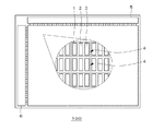
図1は、第1の実施形態の有機EL表示装置の構成について概略的に示す図である。同図に示す有機EL表示装置100は、3つの色画素1、2、3を含んで構成される基本画素4をマトリクス状に多数配列した表示領域を備え、当該表示領域が、データ線駆動回路5及び走査線駆動回路6によって線順次走査方式で駆動されて画像表示を行うものである。各色画素は、例えば、色画素1が赤色、色画素2が緑色、色画素3が青色に対応している。各画素4は、複数の薄膜トランジスタ(TFT)を含んで構成される駆動回路を内蔵した回路チップを用いて駆動される。
<First Embodiment>
FIG. 1 is a diagram schematically showing the configuration of the organic EL display device according to the first embodiment. The organic
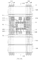
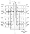
図2は、第1の実施形態における基本画素4の構造について説明する平面図であり、垂直走査方向に隣接配置される2つの基本画素4についての図を示している。なお、図2では説明の便宜上、構成要素の一部を省略して示している。図3は、基本画素4の構造について説明する断面図であり、図2におけるIII−III断面に対応している。
FIG. 2 is a plan view for explaining the structure of the
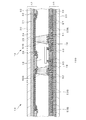
図3に示すように、本実施形態の有機EL表示装置100は、走査線やデータ線等の配線を備えるとともに上面に薄膜状の回路チップ(以下「薄膜回路チップ」という。)16が実装された配線基板10と、色画素を構成する有機EL素子14を備える表示素子基板12とを対向配置し、両者間を銀ペースト等の導電性部材18によって電気的に接続して構成されている。配線基板10と表示素子基板12との相互間にはアクリル樹脂等が適宜充填される。この有機EL表示装置100では、配線基板10側の薄膜回路チップ16によって、表示素子基板12側の各有機EL素子14を駆動している。図示の有機EL素子14が3つ1組となって1つの画素(基本画素4)を構成しており、垂直走査方向に隣接配置される2つの基本画素4に対応する画素駆動回路が1つの薄膜回路チップ16に含まれている。そして、薄膜回路チップ16は、隣接配置される2つの基本画素4の境界付近に配置されている。なお、図2では、表示素子基板12等が省略され、配線基板10の平面図(薄膜回路チップを除く)が示されている。配線基板10上への薄膜回路チップ16の形成は、例えば上述した特許文献1「特開平10−125931号公報」等に開示されるデバイス転写技術を用いて行われる。
As shown in FIG. 3, the organic
配線基板10は、ガラス基板或いはフレキシブル基板等からなる基材20と、当該基材20上に形成された酸化硅素膜等の絶縁膜21、22と、絶縁膜21、22の内部に設けられたアルミニウム膜等の配線(詳細は後述する)とを含んで構成される。上述した薄膜回路チップ16は、ニッケル等からなる接続端子63を介して配線基板10側の配線と電気的に接続される。
The
表示素子基板12は、ガラス基板或いはフレキシブル基板等の透明基材30と、ITO等の透明導電膜からなり透明基材30上に設けられる透明電極(アノード)31と、当該透明電極31上にポリイミド等の絶縁物を用いて形成されており、所定位置に開口を有するバンク(隔壁)32、33と、当該バンク32、33の開口内に形成された正孔注入層34及び発光層35と、アルミニウム等からなり発光層35の上面に形成される電極(カソード)36と、を含んで構成されている。アノード31、正孔注入層34、発光層35及びカソード36を含んで有機EL素子14が構成されており、発光層35に電流を供給することにより当該発光層35から光が放出され、アノード31及び透明基材30を介して外部に放出される。すなわち、本例の有機EL表示装置100はいわゆるトップエミッション構造を採用している。上述した正孔輸送層34は、例えばポリエチレンジオキシチオフェンとポリスチレンスルフォン酸の混合体(PEDOT/PSS)を用いて形成され、発光層35は例えばポリジアルキルフルオレン誘導体を用いて形成される。
The
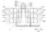
次に、主に図2を参照しながら配線基板10について更に詳細に説明する。図示のように、配線基板10上には、上述したデータ線駆動回路5と接続される複数のデータ線41R、41G、41Bと、電源引き込み用に用いられる引込配線43R、43G、43Bと、上述した走査線駆動回路6と接続される複数の走査線51、52と、図示しない電源と接続される電源線53R、53G、53Bと、各有機EL素子14と配線基板10との電気的接続を担う電極パッド(接続端子)61R、61G、61B、62R、62G、62Bと、薄膜回路チップ16と配線基板10との電気的接続を担う14個の電極パッド(接続端子)63と、を含んで構成されている。データ線41R等及び引込配線43Rを含んで第1配線層が構成され、基材20上に配置されている。また、走査線51等及び電源線53R等を含んで第2配線層が構成され、上記第1配線層の上側に配置されている。上述した薄膜回路チップ16は、図中、点線で示すように電極パッド63の上側に配置される。
Next, the
データ線41R等は、有機EL素子14の駆動に用いるデータ信号を薄膜回路チップ16に供給するためのものであり、アルミニウム等の導電体膜からなる。これらのデータ線41R等は、第2配線層に含まれる補助配線と接続されており、当該補助配線を介して所定の電極パッド63と接続されている。これらのデータ線41R等は、垂直走査方向(線順次走査の進行方向)に沿って隣接配置される各基本画素4によって共用される。データ線41Rが色画素1(赤色)に対応し、データ線41Gが色画素2(緑色)に対応し、データ線41Bが色画素3(青色)に対応している。
The data lines 41R and the like are for supplying a data signal used for driving the
引込配線43R等は、電源線53R等を介して供給される電力を薄膜回路チップ16に伝達するために便宜上用いられるものであり、アルミニウム等の導電体膜からなる。これらの引込配線43R等は、第2配線層に含まれる補助配線と接続されており、当該補助配線を介して所定の電極パッド63と接続されている。これらの引込配線43R等は、垂直走査方向(線順次走査の進行方向)に沿って隣接配置される各基本画素4によって共用される。引込配線43Rが色画素1(赤色)に対応し、引込配線43Gが色画素2(緑色)に対応し、引込配線43Bが色画素3(青色)に対応している。
The lead-in
走査線51等は、有機EL素子14の駆動に用いる走査信号を薄膜回路チップ16に供給するためのものであり、アルミニウム等の導電体膜からなる。これらの走査線51等は、第1配線層に含まれる補助配線と接続されており、当該補助配線を介して所定の電極パッド63と接続されている。走査線51、52のそれぞれは、水平走査方向に沿って隣接配置される一列分の各基本画素4によって共用される。
The
電源線53R等は、図示しない電源と接続され、有機EL素子14を発光させるための電力を薄膜回路チップ16に供給するためのものであり、アルミニウム等の導電体膜からなる。これらの電源線53R等は、第1配線層に含まれる引込配線42R等及び第2配線層に含まれる補助配線を介して所定の電極パッド63と接続されている。そして、これらの電源線53R等のそれぞれは、水平走査方向に沿って隣接配置される二列分の各基本画素4によって共用される。電源線53Rが色画素1(赤色)に対応し、電源線53Gが色画素2(緑色)に対応し、電源線53Bが色画素3(青色)に対応している。
The
図4は、薄膜回路チップ16に含まれる回路の例を説明する図である。また、図5は、図4に示す薄膜回路チップ16のより具体的な構成例(薄膜回路のレイアウト例)を示す図である。図6は、図5に示す薄膜回路の部分的な拡大図である。これらの図に示す駆動回路は、スイッチングトランジスタ、ドライビングトランジスタ及び保持容量を各1つずつ含んで一の有機EL素子14に対応する画素駆動回路が構成されており、当該有機EL素子14に流す電流を制御する機能を有する。ドライビングトランジスタ(第1のトランジスタ)は有機EL素子14に流れる電流を制御するものであり、スイッチングトランジスタ(第2のトランジスタ)はドライビングトランジスタをデータ信号に応じて動作させるものである。
FIG. 4 is a diagram for explaining an example of a circuit included in the thin
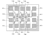
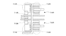
具体的には、スイッチングトランジスタ71R、ドライビングトランジスタ72R及び保持容量73Rを組み合わせて色画素1に対応する有機EL素子14の画素駆動回路74Rが構成され、スイッチングトランジスタ71G、ドライビングトランジスタ72G及び保持容量73Gを組み合わせて色画素2に対応する有機EL素子14の画素駆動回路74Gが構成され、スイッチングトランジスタ71B、ドライビングトランジスタ72B及び保持容量73Bを組み合わせて色画素3に対応する有機EL素子14の画素駆動回路74Bが構成されている。これら3つの画素駆動回路を含んで一の基本画素4の画素駆動回路が構成されている。そして、当該回路において各スイッチングトランジスタ71R、71G、71Bのゲートが共通化されており、外部接続端子としての電極パッド80aが設けられている。この電極パッド80aは、配線基板10側に対向配置される一の電極パッド63と当接することにより薄膜回路チップ16と走査線51との電気的接続を担うものであり、一の基本画素に対応する3つの画素駆動回路74R、74G、74Bごとに共用されて1つ設けられている。
Specifically, the
同様に、スイッチングトランジスタ75R、ドライビングトランジスタ76R及び保持容量77Rを組み合わせて色画素1に対応する有機EL素子14の画素駆動回路78Rが構成され、スイッチングトランジスタ75G、ドライビングトランジスタ76G及び保持容量77Gを組み合わせて色画素2に対応する有機EL素子14の画素駆動回路78Gが構成され、スイッチングトランジスタ75B、ドライビングトランジスタ76B及び保持容量77Bを組み合わせて色画素3に対応する有機EL素子14の画素駆動回路78Bが構成されている。これら3つの画素駆動回路を含んで一の基本画素4の画素駆動回路が構成されている。そして、当該回路において各スイッチングトランジスタのゲートが共通化されており、当該回路において各スイッチングトランジスタ75R、75G、75Bのゲートが共通化されており、外部接続端子としての電極パッド80bが設けられている。この電極パッド80bは、配線基板10側に対向配置される一の電極パッド63と当接することにより薄膜回路チップ16と走査線52との電気的接続を担うものであり、一の基本画素に対応する3つの画素駆動回路78R、78G、78Bごとに共用されて1つ設けられている。
Similarly, the
また、隣接する2つの基本画素4に対応する2つの画素駆動回路において、スイッチングトランジスタ71Rと75R、スイッチングトランジスタ71Gと75G、スイッチングトランジスタ71Bと75Bのそれぞれについてソースが共通化されており、外部接続端子としての電極パッド80c、80d、80eがそれぞれ設けられている。これらの電極パッド80c等は、配線基板10側に対向配置される各電極パッド63とそれぞれ当接することにより薄膜回路チップ16と各データ線41R、41G、41Bのそれぞれとの電気的接続を担うものであり、薄膜回路チップ16内の各駆動回路のうちで隣接配置される2つの基本画素内の同色の色画素のそれぞれに対応する2つの駆動回路ごとに共用されて設けられている。詳細には、画素駆動回路74R及び78Rにより電極パッド80cが共用され、画素駆動回路74G及び78Gにより電極パッド80dが共用され、画素駆動回路74B及び78Bにより電極パッド80eが共用されている。
Further, in two pixel driving circuits corresponding to two adjacent
また、隣接する2つの基本画素4に対応する2つの画素駆動回路において、ドライビングトランジスタ72Rと76R、ドライビングトランジスタ72Gと76G、ドライビングトランジスタ72Bと76B、のそれぞれについてソースが共通化されており、外部接続端子としての電極パッド80f、80g、80hがそれぞれ設けられている。これらの電極パッド80f等は、配線基板10側に対向配置される各電極パッド63のそれぞれと当接することにより、薄膜回路チップ16と各電源線42R、42G、42Bのそれぞれとの電気的接続を担うものであり、薄膜回路チップ16内の各駆動回路のうちで隣接配置される2つの基本画素内の同色の色画素のそれぞれに対応する2つの駆動回路ごとに共用されて設けられている、詳細には、画素駆動回路74R及び78Rにより電極パッド80fが共用され、画素駆動回路74G及び78Gにより電極パッド80gが共用され、画素駆動回路74B及び78Bにより電極パッド80hが共用されている。
Further, in the two pixel driving circuits corresponding to the two adjacent
また、各ドライビングトランジスタ74R、74G、74B、78R、78G、78Bのドレインに対して、各電極パッド80i、80j、80k、80m、80n、80pがそれぞれ設けられている。これらの電極パッド80i等が配線基板10側に対向配置される各電極パッド63と当接することにより、各有機EL素子14に対して電流が供給される。
In addition,
このように、本実施形態では、隣接する2画素に着目し、これらに含まれる各有機EL素子14のそれぞれに対する駆動回路(画素駆動回路)を1つの薄膜回路チップ16に集約することにより、転写技術やその他の実装技術を用いて薄膜回路チップ16を形成する際の実装回数(転写回数)を削減している。また、駆動回路の集約に伴い、薄膜回路チップ16に含まれる画素駆動回路のうち共通化が可能なものについては適宜共通配線とすることにより、当該薄膜回路チップ16と外部との電気的接続を担う電極パッドの数を削減し、チップ面積の縮小を図っている。これらにより、単位面積当たりに製造可能なチップ数が増加し、かつチップの実装回数が削減されるので、有機EL表示装置の製造コストを削減することが可能となる。
As described above, in the present embodiment, attention is paid to two adjacent pixels, and the drive circuit (pixel drive circuit) for each of the
また、本実施形態では、電源線の共用化によって当該電源線を配置可能な面積を増加させることが可能となり、各電源線を広幅化することができる。これにより、電源線を介して電力供給を行う際の電圧降下による影響を低減することが可能となる。 Further, in the present embodiment, by sharing the power supply line, it is possible to increase an area where the power supply line can be arranged, and each power supply line can be widened. Thereby, it becomes possible to reduce the influence by the voltage drop at the time of supplying electric power through the power supply line.
<第2の実施形態>
第2の実施形態として、複数の基本画素のうち水平走査方向に隣接する2つの画素、すなわち走査タイミングが同じであり、かつ相互に隣接配置される2つの基本画素ごとに、当該2つの基本画素に含まれる各色画素に対応する有機EL素子のそれぞれを制御するための複数の駆動回路を含む薄膜回路チップを設けるようにした有機EL表示装置を説明する。なお、上記第1の実施形態の有機EL表示装置と重複する内容については適宜説明を省略する。
<Second Embodiment>
As a second embodiment, two basic pixels that are adjacent to each other in the horizontal scanning direction among a plurality of basic pixels, that is, two basic pixels that have the same scanning timing and are arranged adjacent to each other. An organic EL display device in which a thin film circuit chip including a plurality of drive circuits for controlling each of the organic EL elements corresponding to each color pixel included in the pixel will be described. In addition, about the content which overlaps with the organic electroluminescence display of the said 1st Embodiment, description is abbreviate | omitted suitably.
図7は、第2の実施形態における基本画素4の構造について説明する平面図であり、垂直走査方向に隣接配置される2つの基本画素4についての図を示している。なお、図7では説明の便宜上、構成要素の一部を省略して示している。なお、基本画素4の断面構造については上述した図3に示すものと同様でありここでは説明を省略する。
FIG. 7 is a plan view for explaining the structure of the
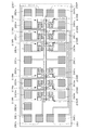
以下、図7を参照しながら、第2の実施形態における配線基板10について詳細に説明する。図示のように、配線基板10上には、上述したデータ線駆動回路5と接続される複数のデータ線141R、141G、141B、143R、143G、143Bと、電源引き込み用に用いられる引込配線142R、142G、142Bと、上述した走査線駆動回路6と接続される走査線151と、図示しない電源と接続される電源線153R、153G、153Bと、各有機EL素子14と配線基板10との電気的接続を担う電極パッド(接続端子)161R、161G、161B、162R、162G、162Bと、薄膜回路チップ116(詳細は後述する)と配線基板10との電気的接続を担う16個の電極パッド(接続端子)163と、を含んで構成されている。データ線141R等及び引込配線142Rを含んで第1配線層が構成され、基材20上に配置されている。また、走査線151等及び電源線153R等を含んで第2配線層が構成され、上記第1配線層の上側に配置されている。上述した薄膜回路チップ116は、電極パッド163の上側に配置される。
Hereinafter, the
データ線141R等は、有機EL素子14の駆動に用いるデータ信号を薄膜回路チップ116に供給するためのものであり、アルミニウム等の導電体膜からなる。これらのデータ線141R等は、第2配線層に含まれる補助配線と接続されており、当該補助配線を介して所定の電極パッド163と接続されている。これらのデータ線141R等は、垂直走査方向(線順次走査の進行方向)に沿って隣接配置される各基本画素4によって共用される。データ線141R、143Rが色画素1(赤色)に対応し、データ線141G、143Gが色画素2(緑色)に対応し、データ線141B、143Bが色画素3(青色)に対応している。
The data lines 141R and the like are for supplying a data signal used for driving the
引込配線142R等は、電源線153R等を介して供給される電力を薄膜回路チップ116に伝達するために便宜上用いられるものであり、アルミニウム等の導電体膜からなる。これらの引込配線142R等は、第2配線層に含まれる補助配線と接続されており、当該補助配線を介して所定の電極パッド163と接続されている。これらの引込配線142R等は、垂直走査方向(線順次走査の進行方向)に沿って隣接配置される各基本画素4によって共用される。引込配線142Rが色画素1(赤色)に対応し、引込配線142Gが色画素2(緑色)に対応し、引込配線142Bが色画素3(青色)に対応している。
The lead-in
走査線151は、有機EL素子14の駆動に用いる走査信号を薄膜回路チップ116に供給するためのものであり、アルミニウム等の導電体膜からなる。なお、同様にして、図示しない走査線が垂直走査方向に沿って複数設けられている。これらの走査線151等は、第1配線層に含まれる補助配線と接続されており、当該補助配線を介して所定の電極パッド163と接続されている。走査線151は、水平走査方向に沿って隣接配置される一列分の各基本画素4によって共用される。本実施形態では、水平走査方向に隣接配置される2つの基本画素4ごとに1つの電極パッド163が割り当てられ、当該電極パッド163を介して走査線151と薄膜回路チップ116とが電気的に接続される。
The
電源線153R等は、有機EL素子14を発光させるための電力を薄膜回路チップ116に供給するためのものであり、アルミニウム等の導電体膜からなる。これらの電源線153R等は、第1配線層に含まれる引込配線142R等及び第2配線層に含まれる補助配線を介して所定の電極パッド163と接続されている。そして、これらの電源線153R等のそれぞれは、水平走査方向に沿って隣接配置される一列分の各基本画素4によって共用される。電源線153Rが色画素1(赤色)に対応し、電源線153Gが色画素2(緑色)に対応し、電源線153Bが色画素3(青色)に対応している。
The
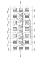
図8は、薄膜回路チップ116に含まれる回路の例を説明する図である。また、図9は、図8に示す薄膜回路チップ116のより具体的な構成例(薄膜回路のレイアウト例)を示す図である。なお、薄膜回路の部分的な拡大図については上記図6に示すものと同様である。これらの図に示す駆動回路は、スイッチングトランジスタ、ドライビングトランジスタ及び保持容量を各1つずつ含んで一の有機EL素子14に対応する画素駆動回路が構成されており、当該有機EL素子14に流す電流を制御する機能を有する。ドライビングトランジスタ(第1のトランジスタ)は有機EL素子14に流れる電流を制御するものであり、スイッチングトランジスタ(第2のトランジスタ)はドライビングトランジスタをデータ信号に応じて動作させるものである。
FIG. 8 is a diagram illustrating an example of a circuit included in the thin
具体的には、図中左側の基本画素4については、色画素1に対応する有機EL素子14の画素駆動回路174Rが構成され、色画素2に対応する有機EL素子14の画素駆動回路174Gが構成され、色画素3に対応する有機EL素子14の画素駆動回路174Bが構成されている。これら3つの画素駆動回路を含んで一の基本画素4の画素駆動回路が構成されている。また、図中右側の基本画素4については、色画素1に対応する有機EL素子14の画素駆動回路178Rが構成され、色画素2に対応する有機EL素子14の画素駆動回路178Gが構成され、色画素3に対応する有機EL素子14の画素駆動回路178Bが構成されている。これら3つの画素駆動回路を含んで一の基本画素4の画素駆動回路が構成されている。各画素駆動回路の詳細内容については上述した第1の実施形態と同様である。そして、当該回路において各スイッチングトランジスタのゲートが共通化されており、外部接続端子としての電極パッド180aが設けられている。この電極パッド180aは、配線基板10側に対向配置される一の電極パッド163と当接することにより薄膜回路チップ116と走査線151との電気的接続を担うものであり、隣接する2つの基本画素4に対応する6つの画素駆動回路ごとに共用されて1つ設けられている。
Specifically, for the
また、隣接する2つの基本画素4に対応する2つの画素駆動回路において、各スイッチングトランジスタのソースに対して外部接続端子としての電極パッド180b、180c、180d、180e、180f、180gがそれぞれ設けられている。これらの電極パッド180b等は、配線基板10側に対向配置される各電極パッド163とそれぞれ当接することにより薄膜回路チップ116と各データ線141R等のそれぞれとの電気的接続を担う。
Further, in two pixel driving circuits corresponding to two adjacent
また、隣接する2つの基本画素4に対応する2つの画素駆動回路における各色画素ごとに各ドライビングトランジスタのソースが共通化されており、外部接続端子としての電極パッド180h、180i、180jがそれぞれ設けられている。これらの電極パッド180h等は、配線基板10側に対向配置される各電極パッド163のそれぞれと当接することにより、薄膜回路チップ116と各電源線142R、142G、142Bのそれぞれとの電気的接続を担うものであり、薄膜回路チップ16内の各駆動回路のうちで隣接配置される2つの基本画素内の同色の色画素のそれぞれに対応する2つの駆動回路ごとに共用されて設けられている、詳細には、画素駆動回路174R及び178Rにより電極パッド180hが共用され、画素駆動回路174G及び178Gにより電極パッド180iが共用され、画素駆動回路174B及び178Bにより電極パッド180jが共用されている。
Further, the source of each driving transistor is made common for each color pixel in two pixel drive circuits corresponding to two adjacent
また、各ドライビングトランジスタのドレインに対して、各電極パッド180k、180m、180n、180p、180q、180rがそれぞれ設けられている。これらの電極パッド180k等が配線基板10側に対向配置される各電極パッド163と当接することにより、各有機EL素子14に対して電流が供給される。
In addition,
このように、本実施形態では、隣接する2画素に着目し、これらに含まれる各有機EL素子14のそれぞれに対する駆動回路(画素駆動回路)を1つの薄膜回路チップ16に集約することにより、転写技術やその他の実装技術を用いて薄膜回路チップ16を形成する際の実装回数(転写回数)を削減している。また、駆動回路の集約に伴い、薄膜回路チップ16に含まれる画素駆動回路のうち共通化が可能なものについては適宜共通配線とすることにより、当該薄膜回路チップ16と外部との電気的接続を担う電極パッドの数を削減し、チップ面積の縮小を図っている。これらにより、単位面積当たりに製造可能なチップ数が増加し、かつチップの実装回数が削減されるので、有機EL表示装置の製造コストを削減することが可能となる。
As described above, in the present embodiment, attention is paid to two adjacent pixels, and the drive circuit (pixel drive circuit) for each of the
<第3の実施形態>
第3の実施形態として、複数の基本画素のうち隣接する4つの画素、より詳細には走査タイミングが同じであり隣接配置される2つの基本画素と、当該2つの基本画素のそれぞれと垂直走査方向に隣接配置される2つの基本画素とを合わせた4つの基本画素ごとに、当該4つの基本画素に含まれる各色画素に対応する有機EL素子のそれぞれを制御するための複数の駆動回路を含む薄膜回路チップを設けるようにした有機EL表示装置を説明する。なお、上記第1又は第2の実施形態の有機EL表示装置と重複する内容については適宜説明を省略する。
<Third Embodiment>
As a third embodiment, four adjacent pixels among a plurality of basic pixels, more specifically, two basic pixels having the same scanning timing and adjacently arranged, and each of the two basic pixels and a vertical scanning direction A thin film including a plurality of drive circuits for controlling each of the organic EL elements corresponding to each color pixel included in the four basic pixels, for every four basic pixels including two basic pixels arranged adjacent to each other An organic EL display device provided with a circuit chip will be described. In addition, about the content which overlaps with the organic electroluminescent display apparatus of the said 1st or 2nd embodiment, description is abbreviate | omitted suitably.
図10は、第3の実施形態における基本画素4の構造について説明する平面図であり、隣接配置される4つの基本画素4についての図を示している。なお、図10では説明の便宜上、構成要素の一部を省略して示している。なお、基本画素4の断面構造については上述した図3に示すものと同様でありここでは説明を省略する。
FIG. 10 is a plan view for explaining the structure of the
以下、図10を参照しながら、第3の実施形態における配線基板10について詳細に説明する。図示のように、配線基板10上には、上述したデータ線駆動回路5と接続される複数のデータ線241R、241G、241B、243R、243G、243Bと、電源引き込み用に用いられる引込配線242R、242G、242Bと、上述した走査線駆動回路6と接続される走査線251、252と、図示しない電源と接続される電源線253R、253G、253Bと、各有機EL素子14と配線基板10との電気的接続を担う電極パッド(接続端子)261R、261G、261B、262R、262G、262B、265R、265G、265B、266R、266G、266Bと、薄膜回路チップ216(詳細は後述する)と配線基板10との電気的接続を担う23個の電極パッド(接続端子)263と、を含んで構成されている。データ線241R等及び引込配線242Rを含んで第1配線層が構成され、基材20上に配置されている。また、走査線251等及び電源線253R等を含んで第2配線層が構成され、上記第1配線層の上側に配置されている。上述した薄膜回路チップ216は、電極パッド263の上側に配置される。
Hereinafter, the
データ線241R等は、有機EL素子14の駆動に用いるデータ信号を薄膜回路チップ216に供給するためのものであり、アルミニウム等の導電体膜からなる。これらのデータ線241R等は、第2配線層に含まれる補助配線と接続されており、当該補助配線を介して所定の電極パッド263と接続されている。これらのデータ線241R等は、垂直走査方向(線順次走査の進行方向)に沿って隣接配置される各基本画素4によって共用される。データ線241R、243Rが色画素1(赤色)に対応し、データ線241G、243Gが色画素2(緑色)に対応し、データ線241B、243Bが色画素3(青色)に対応している。
The data lines 241R and the like are for supplying a data signal used for driving the
引込配線242R等は、電源線253R等を介して供給される電力を薄膜回路チップ216に伝達するために便宜上用いられるものであり、アルミニウム等の導電体膜からなる。これらの引込配線242R等は、第2配線層に含まれる補助配線と接続されており、当該補助配線を介して所定の電極パッド263と接続されている。これらの引込配線242R等は、垂直走査方向(線順次走査の進行方向)に沿って隣接配置される各基本画素4によって共用される。引込配線242Rが色画素1(赤色)に対応し、引込配線242Gが色画素2(緑色)に対応し、引込配線242Bが色画素3(青色)に対応している。
The lead-in
走査線251等は、有機EL素子14の駆動に用いる走査信号を薄膜回路チップ116に供給するためのものであり、アルミニウム等の導電体膜からなる。これらの走査線251等は、第1配線層に含まれる補助配線と接続されており、当該補助配線を介して所定の電極パッド263と接続されている。走査線251等のそれぞれは、水平走査方向に沿って隣接配置される一列分の各基本画素4によって共用される。本実施形態では、水平走査方向に隣接配置される2つの基本画素4ごとに1つの電極パッド263が割り当てられ、当該電極パッド263を介して走査線251等と薄膜回路チップ216とが電気的に接続される。
The
電源線253R等は、有機EL素子14を発光させるための電力を薄膜回路チップ216に供給するためのものであり、アルミニウム等の導電体膜からなる。これらの電源線253R等は、第1配線層に含まれる引込配線242R等及び第2配線層に含まれる補助配線を介して所定の電極パッド263と接続されている。そして、これらの電源線253R等のそれぞれは、水平走査方向に沿って隣接配置される2列分の各基本画素4によって共用される。電源線253Rが色画素1(赤色)に対応し、電源線253Gが色画素2(緑色)に対応し、電源線253Bが色画素3(青色)に対応している。
The
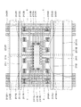
図11は、薄膜回路チップ216に含まれる回路の例を説明する図である。また、図12は、図11に示す薄膜回路チップ216のより具体的な構成例(薄膜回路のレイアウト例)を示す図である。なお、薄膜回路の部分的な拡大図については上記図6に示すものと同様である。これらの図に示す駆動回路は、スイッチングトランジスタ、ドライビングトランジスタ及び保持容量を各1つずつ含んで一の有機EL素子14に対応する画素駆動回路が構成されており、当該有機EL素子14に流す電流を制御する機能を有する。
FIG. 11 is a diagram illustrating an example of a circuit included in the thin
具体的には、図中左上側の基本画素4については、色画素1に対応する有機EL素子14の画素駆動回路274Rが構成され、色画素2に対応する有機EL素子14の画素駆動回路274Gが構成され、色画素3に対応する有機EL素子14の画素駆動回路274Bが構成されている。これら3つの画素駆動回路を含んで一の基本画素4の画素駆動回路が構成されている。また、図中右上側、図中左下側、図中右下側のそれぞれの基本画素4についても、色画素1に対応する有機EL素子14の画素駆動回路278R、294R、298Rがそれぞれが構成され、色画素2に対応する有機EL素子14の画素駆動回路278G、294G、298Gがそれぞれが構成され、色画素3に対応する有機EL素子14の画素駆動回路278B、294B、298Bがそれぞれが構成されている。各画素駆動回路の詳細内容については上述した第1の実施形態と同様である。
Specifically, for the
当該回路において各スイッチングトランジスタのゲートが共通化されており、外部接続端子としての電極パッド280a、280bがそれぞれ設けられている。これらの電極パッド180a等は、配線基板10側に対向配置される一の電極パッド263と当接することにより薄膜回路チップ216と走査線251又は252との電気的接続を担うものであり、隣接する2つの基本画素4に対応する6つの画素駆動回路ごとに共用されて1つ設けられている。
In the circuit, the gates of the switching transistors are shared, and
また、隣接する2つの基本画素4に対応する2つの画素駆動回路において、各スイッチングトランジスタのソースに対して外部接続端子としての電極パッド280c、280d、280e、280f、280g、280hがそれぞれ設けられている。これらの電極パッド280c等は、配線基板10側に対向配置される各電極パッド263とそれぞれ当接することにより薄膜回路チップ216と各データ線241R等のそれぞれとの電気的接続を担う。
Further, in two pixel driving circuits corresponding to two adjacent
また、隣接する2つの基本画素4に対応する2つの画素駆動回路における各色画素ごとに各ドライビングトランジスタのソースが共通化されており、外部接続端子としての電極パッド280i、280j、280kがそれぞれ設けられている。これらの電極パッド280i等は、配線基板10側に対向配置される各電極パッド263のそれぞれと当接することにより、薄膜回路チップ216と各電源線242R、242G、242Bのそれぞれとの電気的接続を担うものであり、薄膜回路チップ216内の各駆動回路のうちで隣接配置される4つの基本画素内の同色の色画素のそれぞれに対応する4つの駆動回路ごとに共用されて設けられている。詳細には、画素駆動回路274R、278R、294R及び298Rにより電極パッド280iが共用され、画素駆動回路274G、278G、294G及び298Gにより電極パッド280jが共用され、画素駆動回路274B、278B、294B及び298Bにより電極パッド280kが共用されている。
Further, the source of each driving transistor is made common for each color pixel in two pixel drive circuits corresponding to two adjacent
また、各ドライビングトランジスタのドレインに対して、各電極パッド280m、280n、280p、280q、280r、280s、280t、280u、280v、280w、280x、280yがそれぞれ設けられている。これらの電極パッド280m等が配線基板10側に対向配置される各電極パッド263と当接することにより、各有機EL素子14に対して電流が供給される。
Also,
このように、本実施形態では、隣接する4画素に着目し、これらに含まれる各有機EL素子14のそれぞれに対する駆動回路(画素駆動回路)を1つの薄膜回路チップ16に集約することにより、転写技術やその他の実装技術を用いて薄膜回路チップ16を形成する際の実装回数(転写回数)を削減している。また、駆動回路の集約に伴い、薄膜回路チップ16に含まれる画素駆動回路のうち共通化が可能なものについては適宜共通配線とすることにより、当該薄膜回路チップ16と外部との電気的接続を担う電極パッドの数を削減し、チップ面積の縮小を図っている。これらにより、単位面積当たりに製造可能なチップ数が増加し、かつチップの実装回数が削減されるので、有機EL表示装置の製造コストを削減することが可能となる。
As described above, in the present embodiment, attention is paid to the four adjacent pixels, and the drive circuit (pixel drive circuit) for each of the
また、本実施形態では、電源線の共用化によって当該電源線を配置可能な面積を増加させることが可能となり、各電源線を広幅化することができる。これにより、電源線を介して電力供給を行う際の電圧降下による影響を低減することが可能となる。 Further, in the present embodiment, by sharing the power supply line, it is possible to increase an area where the power supply line can be arranged, and each power supply line can be widened. Thereby, it becomes possible to reduce the influence by the voltage drop at the time of supplying electric power through the power supply line.
<第4の実施形態>
図13は、上述した各実施形態のいずれかにかかる有機EL表示装置(電気光学装置)を含んで構成される電子機器の具体例を説明する図である。図13(A)は携帯電話への適用例であり、当該携帯電話530はアンテナ部531、音声出力部532、音声入力部533、操作部534、および本発明の電気光学装置100を備えている。このように本発明の電気光学装置は表示部として利用可能である。図13(B)はビデオカメラへの適用例であり、当該ビデオカメラ540は受像部541、操作部542、音声入力部543、および本発明の電気光学装置100を備えている。図13(C)はテレビジョンへの適用例であり、当該テレビジョン550は本発明の電気光学装置100を備えている。なお、パーソナルコンピュータ等に用いられるモニタ装置に対しても同様に本発明に係る電気光学装置を適用し得る。図13(D)はロールアップ式テレビジョンへの適用例であり、当該ロールアップ式テレビジョン560は本発明の電気光学装置100を備えている。また、電子機器はこれらに限定されず、表示機能を有する各種の電子機器に適用可能である。例えばこれらの他に、表示機能付きファックス装置、デジタルカメラのファインダ、携帯型TV、電子手帳、電光掲示盤、宣伝公告用ディスプレイなども含まれる。
<Fourth Embodiment>
FIG. 13 is a diagram for explaining a specific example of an electronic apparatus including the organic EL display device (electro-optical device) according to any of the above-described embodiments. FIG. 13A shows an application example to a mobile phone, and the
<変形実施例>
なお、本発明は上述した各実施形態の内容に限定されるものではなく、本発明の要旨の範囲内において種々の変形実施が可能である。
<Modified Example>
In addition, this invention is not limited to the content of each embodiment mentioned above, A various deformation | transformation implementation is possible within the scope of the summary of this invention.
例えば、上述した実施形態では、電気光学装置の一例として有機EL表示装置を採り上げて説明していたが、本発明を適用可能な電気光学装置はこれに限定されるものではない。複数の色画素を含んでなる基本画素をマトリクス状に複数配列した表示領域を備え、当該表示領域が線順次走査方式で駆動される各種の表示装置(いわゆるアクティブマトリクス型表示装置)に対して本発明を適用することが可能である。 For example, in the above-described embodiment, an organic EL display device has been described as an example of an electro-optical device. However, an electro-optical device to which the present invention can be applied is not limited thereto. The present invention is applied to various display devices (so-called active matrix display devices) having a display region in which a plurality of basic pixels including a plurality of color pixels are arranged in a matrix and the display region is driven by a line-sequential scanning method. The invention can be applied.
また、上述した実施形態では、配線基板と表示素子基板とを貼り合わせた構造の有機EL表示装置を例にして説明していたが、デバイス構造はこれに限定されるものではない。他にも、例えば、一の基板上に、配線を含む層と表示素子を含む層を積層したデバイス構造のもの等に対しても本発明を適用可能である。 In the above-described embodiment, the organic EL display device having a structure in which the wiring substrate and the display element substrate are bonded to each other has been described as an example. However, the device structure is not limited to this. In addition, for example, the present invention can be applied to a device structure in which a layer including wiring and a layer including a display element are stacked on one substrate.
1,2,3…色画素、 4…基本画素、 5…データ線駆動回路、 6…走査線駆動回路、 10…配線基板、 12…表示素子基板、 14…有機EL素子、 16…薄膜回路チップ、 20…基材、 23…接続端子、 41R,41G,41B…データ線、 51,52…走査線、 53R,53G,53B…電源線、 62R,62G,62B…配線基板側の電極パッド(接続端子)、 74R,74G,74B,78R,78G,78B…画素駆動回路、 80a,80b,80c,80d,80e,80f,80g,80h,80i,80j,80k,80m,80n,80p…薄膜回路チップ側の電極パッド(接続端子)
DESCRIPTION OF
Claims (13)
複数の前記色画素を構成する複数の電気光学素子と、
複数の前記基本画素のうち、垂直走査方向に隣接配置される2つの基本画素ごとに1つ設けられ、当該2つの基本画素に含まれる各色画素に対応する電気光学素子のそれぞれを制御するための複数の駆動回路を含む回路チップと、
前記電気光学素子の駆動に用いる走査信号を前記回路チップに供給するための複数の走査線と、
前記電気光学素子の駆動に用いるデータ信号を前記回路チップに供給するための複数のデータ線と、
前記電気光学素子を発光させるための電力を前記回路チップに供給するための複数の電源線と、
前記回路チップと、前記走査線、前記データ線及び前記電源線との相互間に設けられて電気的接続を担う複数の接続端子と、
を含み、
前記回路チップと前記データ線との電気的接続を担う前記接続端子は、前記回路チップ内の各駆動回路のうちで前記隣接配置される2つの基本画素内の同色の色画素のそれぞれに対応する2つの駆動回路ごとに共用されて設けられている、電気光学装置。 An electro-optical device that includes a display area in which a plurality of basic pixels including a plurality of color pixels are arranged in a matrix, and the display area is driven by a line-sequential scanning method.
A plurality of electro-optic elements constituting a plurality of the color pixels;
One of the plurality of basic pixels is provided for every two basic pixels arranged adjacent to each other in the vertical scanning direction, and controls each of the electro-optic elements corresponding to the color pixels included in the two basic pixels. A circuit chip including a plurality of drive circuits;
A plurality of scanning lines for supplying a scanning signal used for driving the electro-optic element to the circuit chip;
A plurality of data lines for supplying a data signal used for driving the electro-optic element to the circuit chip;
A plurality of power supply lines for supplying power for causing the electro-optic element to emit light to the circuit chip;
A plurality of connection terminals that are provided between the circuit chip and the scanning lines, the data lines, and the power supply lines and are in electrical connection;
Including
The connection terminal responsible for electrical connection between the circuit chip and the data line corresponds to each of the same color pixels in the two adjacently arranged basic pixels among the drive circuits in the circuit chip. An electro-optical device provided for each of two driving circuits.
複数の前記色画素を構成する複数の電気光学素子と、
複数の前記基本画素のうち、走査タイミングが同じであり、かつ相互に隣接配置される2つの基本画素ごとに1つ設けられ、当該2つの基本画素に含まれる各色画素に対応する電気光学素子のそれぞれを制御するための複数の駆動回路を含む回路チップと、
前記電気光学素子の駆動に用いる走査信号を前記回路チップに供給するための複数の走査線と、
前記電気光学素子の駆動に用いるデータ信号を前記回路チップに供給するための複数のデータ線と、
前記電気光学素子を発光させるための電力を前記回路チップに供給するための複数の電源線と、
前記回路チップと、前記走査線、前記データ線及び前記電源線との相互間に設けられて電気的接続を担う複数の接続端子と、
を含み、
前記回路チップと前記走査線との電気的接続を担う前記接続端子は、前記回路チップ内の各駆動回路に共用されて設けられている、電気光学装置。 An electro-optical device that includes a display area in which a plurality of basic pixels including a plurality of color pixels are arranged in a matrix, and the display area is driven by a line-sequential scanning method.
A plurality of electro-optic elements constituting a plurality of the color pixels;
Among the plurality of basic pixels, one is provided for each of two basic pixels that have the same scanning timing and are arranged adjacent to each other, and the electro-optic element corresponding to each color pixel included in the two basic pixels A circuit chip including a plurality of drive circuits for controlling each of them;
A plurality of scanning lines for supplying a scanning signal used for driving the electro-optic element to the circuit chip;
A plurality of data lines for supplying a data signal used for driving the electro-optic element to the circuit chip;
A plurality of power supply lines for supplying power for causing the electro-optic element to emit light to the circuit chip;
A plurality of connection terminals that are provided between the circuit chip and the scanning lines, the data lines, and the power supply lines and are in electrical connection;
Including
The electro-optical device, wherein the connection terminal responsible for electrical connection between the circuit chip and the scanning line is provided in common for each drive circuit in the circuit chip.
複数の前記色画素を構成する複数の電気光学素子と、
複数の前記基本画素のうち、走査タイミングが同じであり隣接配置される2つの基本画素と、当該2つの基本画素のそれぞれと垂直走査方向に隣接配置される2つの基本画素とを合わせた4つの基本画素ごとに1つ設けられ、当該4つの基本画素に含まれる各色画素に対応する電気光学素子のそれぞれを制御するための複数の駆動回路を含む回路チップと、
前記電気光学素子の駆動に用いる走査信号を前記回路チップに供給するための複数の走査線と、
前記電気光学素子の駆動に用いるデータ信号を前記回路チップに供給するための複数のデータ線と、
前記電気光学素子を発光させるための電力を前記回路チップに供給するための複数の電源線と、
前記回路チップと、前記走査線、前記データ線及び前記電源線との相互間に設けられて電気的接続を担う複数の接続端子と、
を含み、
前記回路チップと前記走査線との電気的接続を担う前記接続端子は、前記回路チップ内の各駆動回路のうちで、前記走査タイミングが同じであり隣接配置される2つの基本画素内の各駆動回路に共用されて設けられ、
前記回路チップと前記データ線との電気的接続を担う前記接続端子は、前記回路チップ内の各駆動回路のうちで前記垂直走査方向に隣接配置される2つの基本画素内の同色の色画素のそれぞれに対応する2つの駆動回路ごとに共用されて設けられている、電気光学装置。 An electro-optical device that includes a display area in which a plurality of basic pixels including a plurality of color pixels are arranged in a matrix, and the display area is driven by a line-sequential scanning method.
A plurality of electro-optic elements constituting a plurality of the color pixels;
Among the plurality of basic pixels, four basic pixels having the same scanning timing and arranged adjacent to each other, and two basic pixels arranged adjacent to each of the two basic pixels in the vertical scanning direction are combined. A circuit chip including a plurality of drive circuits provided for each basic pixel and controlling each of the electro-optic elements corresponding to the color pixels included in the four basic pixels;
A plurality of scanning lines for supplying a scanning signal used for driving the electro-optic element to the circuit chip;
A plurality of data lines for supplying a data signal used for driving the electro-optic element to the circuit chip;
A plurality of power supply lines for supplying power for causing the electro-optic element to emit light to the circuit chip;
A plurality of connection terminals which are provided between the circuit chip and the scanning lines, the data lines, and the power supply lines and are in electrical connection;
Including
The connection terminal responsible for the electrical connection between the circuit chip and the scanning line is a driving circuit in two basic pixels arranged adjacent to each other in the driving circuit in the circuit chip having the same scanning timing. Provided in common with the circuit,
The connection terminal responsible for electrical connection between the circuit chip and the data line is the same color pixel in two basic pixels arranged adjacent to each other in the vertical scanning direction among the drive circuits in the circuit chip. An electro-optical device provided in common for each of two corresponding drive circuits.
Priority Applications (1)
| Application Number | Priority Date | Filing Date | Title |
|---|---|---|---|
| JP2004109084A JP2005292566A (en) | 2004-04-01 | 2004-04-01 | Electro-optical device and electronic apparatus |
Applications Claiming Priority (1)
| Application Number | Priority Date | Filing Date | Title |
|---|---|---|---|
| JP2004109084A JP2005292566A (en) | 2004-04-01 | 2004-04-01 | Electro-optical device and electronic apparatus |
Publications (1)
| Publication Number | Publication Date |
|---|---|
| JP2005292566A true JP2005292566A (en) | 2005-10-20 |
Family
ID=35325536
Family Applications (1)
| Application Number | Title | Priority Date | Filing Date |
|---|---|---|---|
| JP2004109084A Pending JP2005292566A (en) | 2004-04-01 | 2004-04-01 | Electro-optical device and electronic apparatus |
Country Status (1)
| Country | Link |
|---|---|
| JP (1) | JP2005292566A (en) |
Cited By (4)
| Publication number | Priority date | Publication date | Assignee | Title |
|---|---|---|---|---|
| JP2013502620A (en) * | 2009-08-24 | 2013-01-24 | グローバル・オーエルイーディー・テクノロジー・リミテッド・ライアビリティ・カンパニー | Control of electronic devices using chiplets |
| CN113689796A (en) * | 2020-05-13 | 2021-11-23 | 京东方科技集团股份有限公司 | Array substrate, detection method thereof and spliced display panel |
| CN114566519A (en) * | 2020-11-27 | 2022-05-31 | 京东方科技集团股份有限公司 | Display substrate and display device |
| WO2023184167A1 (en) * | 2022-03-29 | 2023-10-05 | 京东方科技集团股份有限公司 | Display substrate and display apparatus |
-
2004
- 2004-04-01 JP JP2004109084A patent/JP2005292566A/en active Pending
Cited By (7)
| Publication number | Priority date | Publication date | Assignee | Title |
|---|---|---|---|---|
| JP2013502620A (en) * | 2009-08-24 | 2013-01-24 | グローバル・オーエルイーディー・テクノロジー・リミテッド・ライアビリティ・カンパニー | Control of electronic devices using chiplets |
| CN113689796A (en) * | 2020-05-13 | 2021-11-23 | 京东方科技集团股份有限公司 | Array substrate, detection method thereof and spliced display panel |
| US12567357B2 (en) | 2020-05-13 | 2026-03-03 | Boe Technology Group Co., Ltd. | Array substrate and detection method therefor, and tiled display panel |
| CN114566519A (en) * | 2020-11-27 | 2022-05-31 | 京东方科技集团股份有限公司 | Display substrate and display device |
| CN114566519B (en) * | 2020-11-27 | 2026-02-13 | 京东方科技集团股份有限公司 | Display substrate and display device |
| WO2023184167A1 (en) * | 2022-03-29 | 2023-10-05 | 京东方科技集团股份有限公司 | Display substrate and display apparatus |
| US12563939B2 (en) | 2022-03-29 | 2026-02-24 | Chengdu Boe Optoelectronics Technology Co., Ltd. | Display substrate and display device |
Similar Documents
| Publication | Publication Date | Title |
|---|---|---|
| CN110911443B (en) | Tile display device | |
| CN108878444B (en) | Display panel and display device | |
| EP3331019B1 (en) | Display device | |
| CN114784077B (en) | Display panel and display device | |
| KR101383085B1 (en) | Organic light emitting diode display | |
| JP3977299B2 (en) | Electro-optical device, matrix substrate, and electronic apparatus | |
| US20250261529A1 (en) | Display substrate including first reference voltage line being electrically coupled to first reference voltage auxiliary line through via holes penetrating through insulation layer therebetween, and display device having the same | |
| KR20180009441A (en) | Display panel, manufacturing method thereof and display apparatus having the same | |
| US20040061694A1 (en) | Display apparatus where voltage supply region and control circuit therein are stacked | |
| CN111653603A (en) | Display substrate and display device | |
| WO2022007571A1 (en) | Display apparatus and manufacturing method therefor | |
| CN113724592B (en) | A display module and display device | |
| CN114300522A (en) | Display panel, repairing method thereof and display device | |
| CN115377169A (en) | Display substrate and display device | |
| JP2024020328A (en) | Array board and display device | |
| US6573660B2 (en) | Driving emissive displays | |
| US20240096905A1 (en) | Display panel and tiled display screen | |
| CN113764461B (en) | Display panel and display device | |
| JP2005292566A (en) | Electro-optical device and electronic apparatus | |
| US11316002B2 (en) | Unit pixel and organic light emitting display device including the same | |
| CN116917979A (en) | Pixel group, array substrate and display panel | |
| US20240304634A1 (en) | Light emitting display device | |
| US20240258329A1 (en) | Display apparatus | |
| JP2022551619A (en) | Display device and display unit | |
| WO2021024063A1 (en) | Display device |