JP2005292533A - Image forming apparatus - Google Patents
Image forming apparatus Download PDFInfo
- Publication number
- JP2005292533A JP2005292533A JP2004108770A JP2004108770A JP2005292533A JP 2005292533 A JP2005292533 A JP 2005292533A JP 2004108770 A JP2004108770 A JP 2004108770A JP 2004108770 A JP2004108770 A JP 2004108770A JP 2005292533 A JP2005292533 A JP 2005292533A
- Authority
- JP
- Japan
- Prior art keywords
- transfer
- toner
- image
- output
- forming apparatus
- Prior art date
- Legal status (The legal status is an assumption and is not a legal conclusion. Google has not performed a legal analysis and makes no representation as to the accuracy of the status listed.)
- Pending
Links
- 238000012546 transfer Methods 0.000 claims abstract description 189
- 238000000034 method Methods 0.000 claims description 12
- 230000015572 biosynthetic process Effects 0.000 claims description 8
- 238000011161 development Methods 0.000 claims description 8
- 108091008695 photoreceptors Proteins 0.000 claims description 4
- 238000006116 polymerization reaction Methods 0.000 claims description 4
- 239000011347 resin Substances 0.000 claims 1
- 229920005989 resin Polymers 0.000 claims 1
- 239000011362 coarse particle Substances 0.000 abstract description 16
- 239000000126 substance Substances 0.000 abstract 1
- 239000011800 void material Substances 0.000 abstract 1
- 241000519995 Stachys sylvatica Species 0.000 description 15
- 238000004140 cleaning Methods 0.000 description 9
- 238000010438 heat treatment Methods 0.000 description 5
- 239000002245 particle Substances 0.000 description 5
- 239000000463 material Substances 0.000 description 4
- 229910052782 aluminium Inorganic materials 0.000 description 3
- XAGFODPZIPBFFR-UHFFFAOYSA-N aluminium Chemical compound [Al] XAGFODPZIPBFFR-UHFFFAOYSA-N 0.000 description 3
- 238000010586 diagram Methods 0.000 description 3
- 239000000428 dust Substances 0.000 description 3
- 238000002474 experimental method Methods 0.000 description 3
- 230000001360 synchronised effect Effects 0.000 description 3
- 239000004642 Polyimide Substances 0.000 description 2
- 239000000654 additive Substances 0.000 description 2
- 230000000996 additive effect Effects 0.000 description 2
- 230000006870 function Effects 0.000 description 2
- 230000003472 neutralizing effect Effects 0.000 description 2
- 229920001721 polyimide Polymers 0.000 description 2
- 238000003825 pressing Methods 0.000 description 2
- YCKRFDGAMUMZLT-UHFFFAOYSA-N Fluorine atom Chemical compound [F] YCKRFDGAMUMZLT-UHFFFAOYSA-N 0.000 description 1
- 239000004677 Nylon Substances 0.000 description 1
- 239000002033 PVDF binder Substances 0.000 description 1
- 229910045601 alloy Inorganic materials 0.000 description 1
- 239000000956 alloy Substances 0.000 description 1
- 229910021417 amorphous silicon Inorganic materials 0.000 description 1
- 239000011248 coating agent Substances 0.000 description 1
- 238000000576 coating method Methods 0.000 description 1
- 239000004020 conductor Substances 0.000 description 1
- 239000000470 constituent Substances 0.000 description 1
- 230000006866 deterioration Effects 0.000 description 1
- 230000005684 electric field Effects 0.000 description 1
- 230000008030 elimination Effects 0.000 description 1
- 238000003379 elimination reaction Methods 0.000 description 1
- 229920006351 engineering plastic Polymers 0.000 description 1
- 229920000840 ethylene tetrafluoroethylene copolymer Polymers 0.000 description 1
- 229910052731 fluorine Inorganic materials 0.000 description 1
- 239000011737 fluorine Substances 0.000 description 1
- 229910052736 halogen Inorganic materials 0.000 description 1
- 150000002367 halogens Chemical class 0.000 description 1
- 229910052751 metal Inorganic materials 0.000 description 1
- 239000002184 metal Substances 0.000 description 1
- 238000012544 monitoring process Methods 0.000 description 1
- 229920001778 nylon Polymers 0.000 description 1
- 230000003287 optical effect Effects 0.000 description 1
- 230000002093 peripheral effect Effects 0.000 description 1
- 229920002981 polyvinylidene fluoride Polymers 0.000 description 1
- 239000000843 powder Substances 0.000 description 1
- 239000010935 stainless steel Substances 0.000 description 1
- 229910001220 stainless steel Inorganic materials 0.000 description 1
- 230000003068 static effect Effects 0.000 description 1
- 239000000758 substrate Substances 0.000 description 1
- 229920001187 thermosetting polymer Polymers 0.000 description 1
- 239000002699 waste material Substances 0.000 description 1
Images
Landscapes
- Developing For Electrophotography (AREA)
- Electrostatic Charge, Transfer And Separation In Electrography (AREA)
- Color Electrophotography (AREA)
- Developing Agents For Electrophotography (AREA)
Abstract
Description
本発明は、複写機、プリンタ、FAX等の電子写真方式の画像形成装置に関し、特に重合法にて作成したトナーを使用し、ローラ転写方式の画像形成装置に関する。 The present invention relates to an electrophotographic image forming apparatus such as a copying machine, a printer, and a FAX, and more particularly, to a roller transfer type image forming apparatus using toner prepared by a polymerization method.
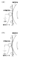
図2は、本発明に係わる転写ローラによる転写領域を示す。 FIG. 2 shows a transfer area by the transfer roller according to the present invention.
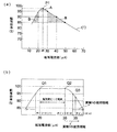
図3は、転写電流と転写効率の関係を示す図である。 FIG. 3 is a diagram showing the relationship between transfer current and transfer efficiency.
中間転写体、像担持体上を転写ローラに電圧を印加することで中間転写体に転写させる手段を有する画像形成装置においては、図3(a)に示す、曲線(1)のような転写効率のピーク値がP1となるような曲線となる。したがって、一般的には転写効率がピークのある領域Aで出力するように選択されている。 In an image forming apparatus having means for transferring a voltage onto an intermediate transfer member by applying a voltage to the transfer roller on the intermediate transfer member and the image carrier, the transfer efficiency as indicated by curve (1) shown in FIG. It becomes a curve that the peak value of becomes P1. Therefore, in general, the output is selected so as to be output in the region A where the transfer efficiency has a peak.
ところが、図2(a)は粒子の大きさが揃ったトナーの転写領域を示しているが、図2(b)で示すように、感光体上に粗大粒子が存在する場合、粗大粒子の周辺部分では画像上に白抜けが発生する場合がある。 However, FIG. 2A shows a toner transfer region having a uniform particle size. As shown in FIG. 2B, when coarse particles are present on the photoreceptor, the periphery of the coarse particles is shown. In some parts, white spots may occur on the image.
重合法によって作られた重合トナーには好ましくない大きさのトナーが混入することがある。通常平均粒径6.5μmとすると10〜100μmの大径トナーが混入する。さらに2成分現像剤の場合には粒径20〜80μm程のキャリアがあり、それが感光体上に付着すると粗大粒子として核となる。さらには、現像器にトナーを補給するトナーボトルやホッパといった部分でトナーを攪拌混合する際に粗大粒子が形成される場合もある。 Undesirably sized toner may be mixed into the polymerized toner produced by the polymerization method. Usually, when the average particle diameter is 6.5 μm, a large diameter toner of 10 to 100 μm is mixed. Further, in the case of a two-component developer, there is a carrier having a particle size of about 20 to 80 μm, and when it is deposited on the photoreceptor, it becomes a nucleus as coarse particles. Furthermore, coarse particles may be formed when the toner is agitated and mixed in a portion such as a toner bottle or a hopper for supplying toner to the developing device.
白抜け現象は、像担持体(感光体/中間転写体)と転写体(中間転写体/記録紙)の間に粗大粒子(キャリア、大径トナー、埃、紙粉等)が存在することで粗大粒子の周辺部分の密着性(像担持体と転写体との)が悪くなりトナーが転写されにくいため発生する。この現象には、粗大粒子の粒径、トナー帯電量、トナー外添剤量、転写電界の大きさ、像担持体および転写体の電気抵抗値、転写体の厚さ、像担持体に対する転写体の押圧力等が関係している。従って、基本的にはこれらの条件を最適化することでこの白抜け現象を軽減できる。一般的には初期トナーの帯電量やトナーの外添剤量、転写体の電気抵抗値等で最適化する。しかし初期的にこれらのパラメータを最適化し、白抜けが発生しない条件に設定できたとしても、プリントの量が進むに従って、耐久的に性能を満足できないことが多い。さらにトナーの帯電量や転写体の電気抵抗値などは白抜け性能だけから最適化できるパラメータではない場合が多い。したがって、粗大粒子を含む現像手段を有する画像形成装置においては、これまでは様々な環境下において白抜けが全く発生しない条件を設定することは不可能である。 The white spot phenomenon is caused by the presence of coarse particles (carrier, large diameter toner, dust, paper dust, etc.) between the image carrier (photosensitive member / intermediate transfer member) and the transfer member (intermediate transfer member / recording paper). This occurs because the adhesion (between the image carrier and the transfer member) of the peripheral portion of the coarse particles is poor and the toner is not easily transferred. This phenomenon includes coarse particle size, toner charge amount, toner external additive amount, transfer electric field strength, image carrier and transfer member electrical resistance, transfer member thickness, transfer member to image carrier. The pressing force is related. Therefore, basically, the white spot phenomenon can be reduced by optimizing these conditions. In general, the initial toner charge amount, the toner external additive amount, the electric resistance value of the transfer member, and the like are optimized. However, even if these parameters are initially optimized and set so that white spots do not occur, the performance cannot often be satisfied as the amount of printing progresses. Furthermore, the charge amount of toner and the electric resistance value of the transfer member are often not parameters that can be optimized only from the whiteout performance. Therefore, in an image forming apparatus having a developing means including coarse particles, it has been impossible to set a condition that no white spots occur under various environments.
そこで、転写体である記録紙等への画像転写開始後の転写部位における転写電圧または転写電流を検出し、その検出値に基づいて転写手段に印加する転写バイアスを補正する方法(例えば、特許文献1参照)や、転写器に供給する電流値を転写効率が最大となるときよりも大きい値に規定する方法(例えば、特許文献2参照)や、転写時におけるトナーの飛び散りや転写不良を減少させるため、特定の粒子形状のトナーを使用して、転写器のコロナ放電ワイヤに流す電流値を、転写効率が最大値になるときよりも大きな値に設定する方法も提案されている(例えば、特許文献3参照)。
しかしながら、上記提案は、コロナ転写方式、転写紙への転写、転写時の電圧や電流をモニタする等に限定し、中間転写体への転写に関しては触れていない。 However, the above proposal is limited to corona transfer system, transfer to transfer paper, monitoring voltage and current during transfer, etc., and does not mention transfer to an intermediate transfer member.
本発明は、像担持体上に形成された、重合トナーによるトナー像を中間転写体に転写する際、粗大粒子を含む重合トナー、キャリア、その他の混入による画像白抜け発生のない、安定した画像を出力する画像形成装置を提供することを目的とする。 The present invention provides a stable image free from the occurrence of white spots caused by mixing of polymerized toner containing coarse particles, a carrier, or the like when transferring a toner image formed of a polymerized toner formed on an image carrier to an intermediate transfer member. An object of the present invention is to provide an image forming apparatus that outputs image data.
上記目的は、以下の構成によって達成することができる。 The above object can be achieved by the following configuration.
(1)像担持体上に形成された、重合トナーによるトナー像を中間転写体に一旦転写し、当該中間転写体から記録紙に一括転写する転写手段を有する画像形成装置において、前記像担持体から前記中間転写体に転写される各色のトナー量が、前記像担持体上に形成されたトナー像の各色のトナー量に対して、85〜95%の転写効率が確保されような領域でそれぞれの転写出力値を決定することを特徴とする画像形成装置(第1の発明)。 (1) In an image forming apparatus having transfer means for temporarily transferring a toner image formed of a polymerized toner formed on an image carrier onto an intermediate transfer member, and transferring the batch from the intermediate transfer member to a recording sheet, the image carrier The toner amount of each color transferred from the toner to the intermediate transfer member is in an area where transfer efficiency of 85 to 95% is ensured with respect to the toner amount of each color of the toner image formed on the image carrier. An image forming apparatus for determining a transfer output value (first invention).
(2)重合トナーを用い、現像バイアスでトナー付着量を調整する方式によって感光体上に形成されたトナー像を一旦中間転写体に転写する画像形成装置において、転写出力に対して転写率がピークに達する点を出力1とし、転写率がピークから降下する点を出力2とすると、画像形成時の転写出力を出力2より大きくしたことを特徴とする画像形成装置(第2の発明)。 (2) In an image forming apparatus in which a toner image formed on a photoconductor is temporarily transferred to an intermediate transfer body by using a polymerized toner and adjusting a toner adhesion amount by a developing bias, the transfer rate peaks with respect to the transfer output. An image forming apparatus characterized in that the transfer output during image formation is larger than output 2 when the point at which the output reaches 1 is output 1 and the point at which the transfer rate drops from the peak is output 2 (second invention).
(3)重合トナーを用い、現像バイアスでトナー付着量を調整する方式によって感光体上に形成されたトナー像を一旦中間転写体に転写する画像形成装置において、転写出力に対して転写率がピークに達する点を出力1、転写率が当該ピークから降下する点を転写出力2とすると、現像材投入直後の最適画像出力時の現像バイアス値V1に対する画像採取時の現像バイアス値V2の値によって転写出力2にプラスする値を決定し、当該転写出力2にプラスする値で画像形成時の転写出力を決定することを特徴とする画像形成装置(第3の発明)。 (3) In an image forming apparatus that uses a polymerized toner and transfers a toner image formed on a photosensitive member to an intermediate transfer member by a method of adjusting the toner adhesion amount with a developing bias, the transfer rate peaks with respect to the transfer output. The point at which the output reaches 1 is the output 1, and the point at which the transfer rate falls from the peak is the transfer output 2. A value that is added to the output 2 is determined, and a transfer output at the time of image formation is determined by a value that is added to the transfer output 2 (third invention).
転写率の最も高い転写出力領域を採用せず、所定の出力領域に限定することによって、画像白抜けの発生を回避することができる。 By not using the transfer output area with the highest transfer rate but limiting to a predetermined output area, it is possible to avoid the occurrence of image blanking.
はじめに、本発明の画像形成装置について説明する。 First, the image forming apparatus of the present invention will be described.
本発明の実施の形態における説明では、本明細書に用いる用語により技術範囲が限定されることはない。 In the description of the embodiment of the present invention, the technical scope is not limited by the terms used in this specification.
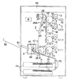
図1は画像形成装置の全体構成の一例を示す模式図である。 FIG. 1 is a schematic diagram illustrating an example of the overall configuration of the image forming apparatus.
図1において、10は像形成体である感光体、11は帯電手段であるスコロトロン帯電器、12はデジタル式像露光手段である書込装置、13は現像手段である現像器、14は感光体10の表面を清掃するためのクリーニング装置、15は感光体10のクリーニング用のブレード、16は現像スリーブ、20は中間転写体である中間転写ベルトを示す。画像形成手段1は感光体10、スコロトロン帯電器11、現像器13、およびクリーニング装置14等からなっており、各色毎の画像形成手段1の機械的な構成は同じであるので、図ではY(イエロー)系列のみの構成について参照符号を付けており、M(マゼンタ)、C(シアン)およびK(黒)の構成要素については参照符号を省略した。
In FIG. 1, 10 is a photoconductor as an image forming body, 11 is a scorotron charger as charging means, 12 is a writing device as digital image exposure means, 13 is a developing device as developing means, and 14 is a photoconductor.
各色毎の画像形成手段1の配置は中間転写ベルト20の走行方向に対して、Y、M、C、Kの順になっており、各感光体10は中間転写ベルト20の張設面に接触し、接触点で中間転写ベルト20の走行方向と同方向、かつ、同線速度で回転する。
The arrangement of the image forming means 1 for each color is in the order of Y, M, C, K with respect to the running direction of the
中間転写ベルト20は駆動ローラ21、アースローラ22、テンションローラ23、除電ローラ27、従動ローラ24に張架され、これらのローラと中間転写ベルト20、転写手段である転写ローラ25、転写補助ローラ25A、クリーニング装置28等でベルトユニット3を構成する。
The
中間転写ベルト20の走行は不図示の駆動モータによる駆動ローラ21の回転によって行われる。
The
感光体10は、例えばアルミ材によって形成される円筒状の金属基体の外周に導電層、a−Si層あるいは有機感光層(OPC)等の感光層を形成したものであり、導電層を接地した状態で図の矢印で示す反時計方向に回転する。
The
読み取り装置80からの画像データに対応する電気信号は、レーザの光信号に変換され、書込装置12によって感光体10上に投光される。
An electrical signal corresponding to the image data from the
現像器13は、感光体10の周面に対し所定の間隔を保ち、感光体10の回転方向と最接近位置において同方向に回転する円筒状の非磁性ステンレスあるいはアルミ材で形成された現像スリーブ16を有し、当該現像器13には不図示のバイアス電源から重合トナーと反対極性のバイアス電圧が印加され、感光体10へのトナーの移行を制御している。
The developing
図1に戻って、中間転写ベルト20は、体積抵抗率106〜1012Ω・cmの樹脂シート状で、強度を有した非弾性素材の無端ベルトであり、例えば変性ポリイミド、熱硬化ポリイミド、エチレンテトラフルオロエチレン共重合体、ポリフッ化ビニリデン、ナイロンアロイ等のエンジニアリングプラスチックに導電材料を分散した、厚さ0.1〜1.0mmの半導電性フィルム基体の外側に、好ましくはトナーフィルミング防止層として厚さ5〜50μmのフッ素コーティングを行った、2層構成のシームレスベルトである。したがって、この素材のベルトは、転写時に中間転写体20と感光体10の間に粗大粒子が存在すると、粒子周辺の中間ベルト20は感光体10に密着しなくなる。
Returning to FIG. 1, the
転写ローラ25には、重合トナーと反対極性の直流が印加され、中間転写ベルト20を感光体10に押圧し、感光体10上に形成されたトナー像を中間転写ベルト20上に転写させる機能を有する。なお、本発明に係わる転写機能については後述する。
A direct current having a polarity opposite to that of the polymerized toner is applied to the
26はアースローラ22から当接および当接解除可能な転写ローラで、中間転写ベルト20上に形成されたトナー像を記録媒体である転写紙Pに再転写する。
28はクリーニング装置で、ベルトクリーニング用のブレード29が中間転写ベルト20を挟んで従動ローラ24に対向して設けられている。
A
トナー像を転写紙Pに転写後、中間転写ベルト20はトナーと同極性または逆極性の直流電圧を重畳した交流電圧が印加された除電ローラ27によって残留トナーの電荷が弱められ、ブレード29によって周面上の残留トナーが清掃される。
After the toner image is transferred onto the transfer paper P, the
40は定着装置で、加熱ローラ41と圧着ローラ42を有している。
A fixing
前記加熱ローラ41は薄手のアルミから形成された円筒状のもので、内側から所定の温度まで加熱するハロゲンヒータ47等を有し、その温度は、前記加熱ローラ41に設置された不図示の接触温度センサにより検出され、制御部Bで温度制御される。
The
次に、図1に基づいて画像形成プロセスを説明する。 Next, the image forming process will be described with reference to FIG.
画像記録のスタートと同時に不図示の感光体駆動モータの始動により色信号Yの感光体10は矢印で示す反時計方向に回転され、同時にスコロトロン帯電器11の帯電作用により感光体10に電位の付与が開始される。
Simultaneously with the start of image recording, the photoconductor drive motor (not shown) starts to rotate the
感光体10は電位を付与されたあと、書込装置12によってYの画像データに対応する画像の書込みが開始され、感光体10の表面に原稿画像のYの画像に対応する静電潜像が形成される。
After the
前記の静電潜像はYの現像器13により非接触の状態で反転現像され、感光体10の回転に応じYのトナー像が感光体10上に形成される。
The electrostatic latent image is reversely developed in a non-contact state by a
当該感光体10上に形成されたYのトナー像は、Yの転写ローラ25の作用により、中間転写ベルト20上に転写される。
The Y toner image formed on the
次いで、書込装置12によってM(マゼンタ)の色信号すなわちMの画像データに対応する画像書き込みが行われ、感光体10の表面に原稿画像のMの画像に対応する静電潜像が形成される。当該静電潜像は、Mの現像器13により感光体10上にMのトナー像となり、Mの転写ローラ25において、中間転写ベルト20上の前記Yのトナー像と同期が取られ、前記Yのトナー像の上に重ね合わされる。
Next, the writing device 12 performs image writing corresponding to an M (magenta) color signal, that is, M image data, and an electrostatic latent image corresponding to the M image of the original image is formed on the surface of the
同様のプロセスにより、Y、Mの重ね合わせトナー像と同期が取られ、C(シアン)のトナー像が、Cの転写ローラ25において、前記のY、Mの重ね合わせトナー像上へ重ね合わされる。次に、すでに形成されているY、M、Cの重ね合わせトナー像と同期が取られ、Kのトナー像が、Kの転写ローラ25において、前記のY、M、Cの重ね合わせトナー像上へ重ね合わされ、Y、M、CおよびKの重ね合わせトナー像が形成される。
By a similar process, the Y and M superimposed toner images are synchronized, and the C (cyan) toner image is superimposed on the Y and M superimposed toner images by the
重ね合わせトナー像が担持されている中間転写ベルト20は矢印W方向に送られ、転写紙Pが紙カセット72より、紙送り出しローラ70によって送り出され、搬送ローラ73を経て、タイミングローラ71へ搬送され、当該タイミングローラ71の駆動によって、中間転写ベルト20上の重ね合わせトナー像と同期がとられて、トナーと反対極性の直流電圧が印加されている転写ローラ26(中間転写ベルト20に当接状態にある)の転写領域Sに給送され、中間転写ベルト20上の重ね合わせトナー像が転写紙Pに転写される。
The
その後、中間転写ベルト20は走行し、除電ローラ27によって残留トナーの電荷が弱められ、クリーニング装置28で当該中間転写ベルト20に当接したブレード29により清掃され、次の画像形成サイクルに入る。
Thereafter, the
掻き落とされたトナーはクリーニング装置28内に溜められ、不図示の搬送スクリューの回転によって軸方向(図において紙表面から紙裏面方向)に搬送し、不図示の廃棄管を介して貯留箱に溜められる。
The toner scraped off is collected in the
重ね合わせトナー像が転写された転写紙Pは、更に定着装置40へと送られ、加熱ローラ41と加圧ローラ42に加熱、加圧され、定着される。トナー像が定着された転写紙Pは、排紙ローラ81によって排紙皿82へ搬送される。
The transfer paper P onto which the superimposed toner image has been transferred is further sent to the fixing
次に、本発明の転写機能について説明する。 Next, the transfer function of the present invention will be described.
重合法によって作られたトナーには、粗大粒子のトナーが混入することがあり、現像器内で当該粗大粒子のトナーおよびキャリア、埃、紙粉等が混合し、現像時にこれらの粗大粒子が感光体上にのトナー像に付着する画像上に白抜けが発生する場合があることは前述した。 The toner produced by the polymerization method may be mixed with toner of coarse particles, and the toner of coarse particles and carrier, dust, paper powder, etc. are mixed in the developing device, and these coarse particles are exposed to light during development. As described above, white spots may occur on the image adhering to the toner image on the body.
本発明では、粗大粒子が存在しても、転写条件によって画像上に白抜けの発生を抑えることができる点を特徴としている。 The present invention is characterized in that even if coarse particles are present, occurrence of white spots on an image can be suppressed depending on transfer conditions.
本発明者は、図3(a)に示す転写出力である転写電流と転写効率を調べる中で、図3(b)に示すように記録紙に転写される直前のトナー量が、像担持体上のから中間転写体への転写効率が最大値なる95%以上の領域A領域を避け、85%以上、95%未満が確保されるの領域Bに対応する転写電流を決定すると、画像上に白抜けの発生を抑えることができることを実験1により確認した。すなわち、転写効率85%以上、95%未満の領域Bに対応する転写電流値で、A領域に対応する転写電流値より大きい転写電流値を決定する(第1の発明)。 While examining the transfer current and transfer efficiency, which are the transfer outputs shown in FIG. 3 (a), the present inventor determines that the amount of toner immediately before being transferred to the recording paper as shown in FIG. When the transfer current corresponding to the region B in which 85% or more and less than 95% are secured is determined while avoiding the region A region of 95% or more where the transfer efficiency to the intermediate transfer member is the maximum value from above, Experiment 1 confirmed that the occurrence of white spots could be suppressed. That is, a transfer current value corresponding to the region B having a transfer efficiency of 85% or more and less than 95% is determined to be larger than the transfer current value corresponding to the A region (first invention).
表1にその実験結果を示す。 Table 1 shows the experimental results.
実験条件として、領域A、領域Bに対応する転写電流が25μA、40μAとして、20万コピーの実写を行った結果、表1のようなデータが得られた。 As experimental conditions, the transfer currents corresponding to the regions A and B were set to 25 μA and 40 μA, and 200,000 copies were actually captured. As a result, data as shown in Table 1 was obtained.

表1において、○:合格レベル、△×:不満足、×:不合格を表す。 In Table 1, ◯: represents a pass level, Δ ×: unsatisfactory, ×: failed.
表からわかるように、転写電流40μAでは、白抜けは合格レベルにあり、25μAでは、合格レベルには達していないことがわかる。 As can be seen from the table, when the transfer current is 40 μA, white spots are at a pass level, and at 25 μA, the pass level is not reached.
したがって、領域Bに対応する転写電流を選択するのが好ましい。 Therefore, it is preferable to select a transfer current corresponding to the region B.
次に、図3(b)において、転写効率がピークに達する点Q1に対応する転写電流をポイント1とし、転写効率がピークから降下する点Q2に対応する転写出電流をポイント2とすると、画像作成時の転写電流をポイント2より大きくすることによって画像白抜けを回避できる(第2の発明)。 Next, in FIG. 3B, when the transfer current corresponding to the point Q1 at which the transfer efficiency reaches a peak is point 1, and the transfer output current corresponding to the point Q2 at which the transfer efficiency drops from the peak is point 2, the image By making the transfer current at the time of creation larger than the point 2, it is possible to avoid white spots in the image (second invention).
ここで、(点Q2における転写電流)+(点Q2における転写電流−Q1における転写電流)/2=Eなる計算式で算出する点Q3をポイント3とすると、ポイント1:20μA、ポイント2:30μA、ポイント3:{30+〔30−20)/2}μA=35μAの転写電流で実験2(コピー数:20万)を行った結果、表2のようなデータが得られた。 Here, assuming that the point Q3 calculated by the formula (transfer current at point Q2) + (transfer current at point Q2−transfer current at Q1) / 2 = E is point 3, point 1:20 μA, point 2:30 μA , Point 3: Experiment 2 (copy number: 200,000) was performed at a transfer current of {30+ [30-20) / 2} μA = 35 μA. As a result, data as shown in Table 2 was obtained.
表2において、○:合格レベル、△○:不満足なるが合格レベル、△×:不満足、×:不合格を表す。 In Table 2, ◯: acceptable level, Δ ◯: unsatisfactory but acceptable level, Δ ×: unsatisfactory, ×: unacceptable.
表2からわかるように、点Q3に対応する転写電流35μAでは白抜けは合格レベルにあり、20〜30μAでは、合格レベルには達していないことがわかる。 As can be seen from Table 2, it is found that the white spot is at a pass level at a transfer current of 35 μA corresponding to the point Q3, and the pass level is not reached at 20 to 30 μA.
したががって、計算式Eで求めた転写電流に対応する転写効率は90%が確保でき、且つ、白抜けも合格レベルとなることがわかる。 Therefore, it can be seen that 90% of the transfer efficiency corresponding to the transfer current obtained by the calculation formula E can be secured, and the white spot is also at a pass level.
次に、本画像形成装置では現像バイアスでトナー付着量を調整する方式によって感光体上に形成されたトナー像のトナー濃度を調整している。 Next, in this image forming apparatus, the toner density of the toner image formed on the photoconductor is adjusted by a method of adjusting the toner adhesion amount by the developing bias.
すなわち、現像材はコピー量が進むに従って劣化するので、トナーの摩擦帯電効率も変化するので、現像バイアスを劣化に応じ変化させるとともに、転写時の
転写電流を変える必要がある。
That is, since the developer deteriorates as the copy amount advances, the triboelectric charging efficiency of the toner also changes. Therefore, it is necessary to change the developing bias according to the deterioration and change the transfer current at the time of transfer.
なお、現像バイアスに対する最適の転写電流についてのプログラムは、制御部Bのメモリ基板に記憶され、当該制御部Bは、現像バイアスに対応した転写電流を出力するように不図示の高圧電源ユニットに指令する方式がとられている。 The program for the optimum transfer current for the developing bias is stored in the memory board of the control unit B, and the control unit B instructs a high-voltage power supply unit (not shown) to output the transfer current corresponding to the developing bias. The method to take is taken.
第3の発明は、転写出力である転写電流に対して転写率がピークに達する点を出力1(I1)、転写率が当該ピークから降下する点を転写出力2(I2)とすると、現像材投入直後の最適画像出力時の現像バイアス値V1に対する画像採取時の現像バイアス値V2の値によって転写出力2(I2)にプラスする値を決定し、当該転写出力2(I2)にプラスした値で画像形成時の転写出力(It)を決定することを特徴とする。 According to a third aspect of the present invention, when a point at which the transfer rate reaches a peak with respect to a transfer current as a transfer output is output 1 (I1) and a point at which the transfer rate falls from the peak is a transfer output 2 (I2), a developer A value to be added to the transfer output 2 (I2) is determined by the value of the development bias value V2 at the time of image acquisition with respect to the development bias value V1 at the time of optimum image output immediately after the input, and a value that is added to the transfer output 2 (I2). The transfer output (It) at the time of image formation is determined.
図3(b)において、点Q1に対応する転写電流をI1、点Q2に対応する転写電流I2、現像材投入直後(攪拌がされていない現像材)に印加される現像バイアス値をVbf、画像形成時の現像バイアス値をVb、最低現像バイアス値をVbminとし、画像形成時の転写電流It=I2+{(Vb−Vbmin)/Vbf−Vbmin)}×(I2−I1)として、実験3(コピー数:20万)を行った結果、表3のようなデータが得られた。 In FIG. 3B, the transfer current corresponding to the point Q1 is I1, the transfer current I2 corresponding to the point Q2, the development bias value applied immediately after supplying the developer (undeveloped developer) is Vbf, and the image The development bias value at the time of formation is Vb, the minimum development bias value is Vbmin, and the transfer current It = I2 + {(Vb−Vbmin) / Vbf−Vbmin)} × (I2−I1) at the time of image formation is experiment 3 (copy) As a result of performing (number: 200,000), data as shown in Table 3 was obtained.
表3において、○:合格レベル、△×:不満足、×:不合格を表す。
表3からわかるように、転写効率のピーク領域に対応する転写電流では、すべて不合格レベルの白抜けが発生しているが、現像バイアス値によりトナー付着量を調整する機械においては、転写効率が85%以上が確保でき、且つ画像白抜けが発生しないことが判明した。
In Table 3, o: pass level, Δx: unsatisfactory, x: fail.
As can be seen from Table 3, in the transfer current corresponding to the peak area of the transfer efficiency, all white spots at the reject level are generated. However, in the machine that adjusts the toner adhesion amount by the developing bias value, the transfer efficiency is low. It was found that 85% or more can be secured, and no white spots occur in the image.
以上、本発明によって、粗大粒子を含むトナー(現像材)を使用する画像形成装置における画像白抜けの発生が回避できることが判明した。 As described above, it has been found that the present invention can avoid the occurrence of image blanking in an image forming apparatus using toner (developer) containing coarse particles.
なお、本実施の形態では、転写出力を電流値で説明したが、電圧値でも同じことがいえる。 In the present embodiment, the transfer output is described as a current value, but the same can be said for a voltage value.
10 感光体
13 現像器
16 現像スリーブ
20 中間転写ベルト
25 転写ローラ
25A 転写補助ローラ
DESCRIPTION OF
Claims (5)
転写出力に対して転写率がピークに達する点を出力1とし、転写率がピークから降下する点を出力2とすると、画像形成時の転写出力を出力2より大きくしたことを特徴とする画像形成装置。 In an image forming apparatus that uses a polymerized toner and temporarily transfers a toner image formed on a photoreceptor by a method of adjusting a toner adhesion amount with a developing bias to an intermediate transfer member,
Image formation characterized in that the transfer output at the time of image formation is larger than output 2 when the point at which the transfer rate reaches the peak with respect to the transfer output is output 1 and the point at which the transfer rate falls from the peak is output 2. apparatus.
Priority Applications (1)
| Application Number | Priority Date | Filing Date | Title |
|---|---|---|---|
| JP2004108770A JP2005292533A (en) | 2004-04-01 | 2004-04-01 | Image forming apparatus |
Applications Claiming Priority (1)
| Application Number | Priority Date | Filing Date | Title |
|---|---|---|---|
| JP2004108770A JP2005292533A (en) | 2004-04-01 | 2004-04-01 | Image forming apparatus |
Publications (1)
| Publication Number | Publication Date |
|---|---|
| JP2005292533A true JP2005292533A (en) | 2005-10-20 |
Family
ID=35325506
Family Applications (1)
| Application Number | Title | Priority Date | Filing Date |
|---|---|---|---|
| JP2004108770A Pending JP2005292533A (en) | 2004-04-01 | 2004-04-01 | Image forming apparatus |
Country Status (1)
| Country | Link |
|---|---|
| JP (1) | JP2005292533A (en) |
-
2004
- 2004-04-01 JP JP2004108770A patent/JP2005292533A/en active Pending
Similar Documents
| Publication | Publication Date | Title |
|---|---|---|
| JP4985146B2 (en) | Image forming apparatus | |
| US20080118272A1 (en) | Image forming apparatus | |
| JP2006259305A (en) | Image forming apparatus | |
| JP2009116096A (en) | Image forming apparatus | |
| US6816697B2 (en) | Image forming apparatus with cleaning unit | |
| JP2005115197A (en) | Image forming apparatus | |
| JP2005292533A (en) | Image forming apparatus | |
| JPH117200A (en) | Image forming device | |
| JP4523354B2 (en) | Image forming apparatus | |
| JP5056202B2 (en) | Image forming apparatus | |
| JP2001265110A (en) | Image forming device | |
| JP2007148165A (en) | Image forming apparatus | |
| JP2007178731A (en) | Cleaning device and image forming apparatus | |
| JP2006259103A (en) | Image forming apparatus | |
| JP2000267530A (en) | Image forming device | |
| JP5151703B2 (en) | Image forming apparatus | |
| JP2007171752A (en) | Image forming apparatus | |
| JP2005114802A (en) | Image forming apparatus and image forming method | |
| US20030231892A1 (en) | Image forming apparatus | |
| JP6187149B2 (en) | Image forming apparatus and program | |
| JP2006227159A (en) | Image forming apparatus | |
| JPH07248672A (en) | Development device | |
| JP2006276681A (en) | Cleaning device for electrophotographic apparatus | |
| JP2008185883A (en) | Image forming apparatus | |
| JP2001290377A (en) | Image forming device |
Legal Events
| Date | Code | Title | Description |
|---|---|---|---|
| A621 | Written request for application examination |
Free format text: JAPANESE INTERMEDIATE CODE: A621 Effective date: 20061114 |
|
| A977 | Report on retrieval |
Free format text: JAPANESE INTERMEDIATE CODE: A971007 Effective date: 20090416 |
|
| A131 | Notification of reasons for refusal |
Free format text: JAPANESE INTERMEDIATE CODE: A131 Effective date: 20090428 |
|
| A02 | Decision of refusal |
Free format text: JAPANESE INTERMEDIATE CODE: A02 Effective date: 20090908 |