JP2005292389A - Electrooptical display device - Google Patents
Electrooptical display device Download PDFInfo
- Publication number
- JP2005292389A JP2005292389A JP2004106019A JP2004106019A JP2005292389A JP 2005292389 A JP2005292389 A JP 2005292389A JP 2004106019 A JP2004106019 A JP 2004106019A JP 2004106019 A JP2004106019 A JP 2004106019A JP 2005292389 A JP2005292389 A JP 2005292389A
- Authority
- JP
- Japan
- Prior art keywords
- wiring board
- trunk
- branch
- terminal
- display device
- Prior art date
- Legal status (The legal status is an assumption and is not a legal conclusion. Google has not performed a legal analysis and makes no representation as to the accuracy of the status listed.)
- Withdrawn
Links
- 239000000758 substrate Substances 0.000 claims abstract description 26
- 239000004973 liquid crystal related substance Substances 0.000 abstract description 36
- 238000000605 extraction Methods 0.000 description 5
- 238000000034 method Methods 0.000 description 2
- 239000004820 Pressure-sensitive adhesive Substances 0.000 description 1
- 238000012986 modification Methods 0.000 description 1
- 230000004048 modification Effects 0.000 description 1
- 230000003287 optical effect Effects 0.000 description 1
Images


Landscapes
- Combinations Of Printed Boards (AREA)
- Devices For Indicating Variable Information By Combining Individual Elements (AREA)
- Liquid Crystal (AREA)
- Structure Of Printed Boards (AREA)
Abstract
Description
本発明は表示パネルの端子部にフレキシブル配線板を接続してなる電気光学表示装置に関し、さらに詳しく言えば、一方の基板側の少なくとも対向する2辺に端子部が設けられている表示パネルに適用されるフレキシブル配線板に関するものである。 The present invention relates to an electro-optical display device in which a flexible wiring board is connected to a terminal portion of a display panel. More specifically, the present invention is applied to a display panel in which terminal portions are provided on at least two opposing sides on one substrate side. The present invention relates to a flexible wiring board.
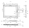
液晶パネルはパネル面内の表示用電極から引き出された引出電極を有する端子部を備えている。その端子部には液晶パネルに駆動信号を与えるためのフレキシブル配線板が接続される。液晶パネルには端子部が1つである1方向取り出し型,端子部を2つ備える2方向取り出し型,端子部を3つ備える3方向取り出し型などがあるが、2方向取り出し型,3方向取り出し型のうちでその各端子部が一方の透明電極基板側のみに設けられる場合がある。その一例を図9に模式的に示す。 The liquid crystal panel includes a terminal portion having an extraction electrode extracted from the display electrode in the panel surface. A flexible wiring board for supplying a drive signal to the liquid crystal panel is connected to the terminal portion. Liquid crystal panels include a one-way extraction type with one terminal part, a two-way extraction type with two terminal parts, and a three-way extraction type with three terminal parts. In the mold, each terminal portion may be provided only on one transparent electrode substrate side. An example thereof is schematically shown in FIG.
この例は特許文献1に記載されている2方向取り出し型についてのもので、図9(a)は平面図,(b)は底面図,(c)は側面図である。液晶パネル10には液晶層を挟んで対向的に配置される2枚の透明電極基板、すなわち観察面側の透明電極基板11と反観察面側(裏面側)の透明電極基板12とが含まれるが、この例では反観察面側の透明電極基板12の対向する2辺に端子部12a,12bが設けられており、その各々に表示データ処理用などのチップ部品(例えばICのベアチップ)CHが実装されている。
This example is for the two-way extraction type described in Patent Document 1, FIG. 9A is a plan view, FIG. 9B is a bottom view, and FIG. 9C is a side view. The
液晶パネル10に駆動信号を与えるため、図9(a)に示すように各端子部12a,12bにフレキシブル配線板20a,20bの各一端が例えば異方性導電フィルム(ACF)などを介して接続されるが、このままでは液晶パネル10をディスプレイ機器に組み込む場合、フレキシブル配線板20a,20bの配線処理を個別的に行うことになり、その作業に手間がかかるばかりでなく配線スペースも必要となる、などの不都合が生ずる。
In order to give a driving signal to the
そこで、この従来例では図9(b)に示すように透明電極基板12の裏面側に液晶駆動回路やバックライト駆動回路などを含む制御回路基板21を配置し、上記フレキシブル配線板20a,20bの各他端側を透明電極基板12の裏面側に折り曲げて制御回路基板21に接続し、これとは別にパネル外に引き出されるコネクタ用のフレキシブル配線板20cを制御回路基板21に接続するようにしている。
Therefore, in this conventional example, as shown in FIG. 9B, a
上記従来例によれば、液晶パネル10をディスプレイ機器に組み込む際にコネクタ用のフレキシブル配線板20cをそのディスプレイ機器側に設けられているソケットなどに差し込めばよく、作業性が改善されるとともに配線スペースも小さくて済む。
According to the above conventional example, when the
しかしながら、パネルメーカ側ではフレキシブル配線板20a,20bについては接続箇所がそれぞれ2箇所,フレキシブル配線板20cについては接続箇所が1箇所で合計5箇所において接続作業を行う必要がある。また、各フレキシブル配線板20a〜20cはそれぞれ個別的に作製されているため部品管理なども煩雑になる。
However, on the panel manufacturer side, it is necessary to perform the connection work at five places in total, with two connection places for the
なお、図10に示すように上記フレキシブル配線板20a〜20cを含む1枚のフレキシブル配線板から打ち抜かれたT字状のフレキシブル配線板20を用いれば、接続箇所は2箇所で済み、また、部品管理も容易となる。
In addition, if the T-shaped
しかしながら、この場合にはフレキシブル配線板20を上記透明電極基板12の裏面側に配置し、フレキシブル配線板20a,20bの各一端を端子部12a,12b側に折り曲げて接続することになるが、実際問題としてその接続しろはわずか(例えば2mm程度)であり、また、折り曲げ部には復元力が発生するため接続作業が困難となり実用的とは言えない。
However, in this case, the
したがって、本発明の課題は、一方の基板側に複数の端子部が設けられている表示パネルに対してフレキシブル配線板を接続してなる電気光学表示装置において、フレキシブル配線板の接続作業性の改善を図ることにある。 Accordingly, an object of the present invention is to improve connection workability of a flexible wiring board in an electro-optic display device in which a flexible wiring board is connected to a display panel having a plurality of terminal portions on one substrate side. Is to plan.
上記課題を解決するため、本願の請求項1に係る発明は、2枚の基板のうちの一方の基板の対向する2辺に端子部を有する表示パネルと、上記端子部の各々に接続されるフレキシブル配線板とを含む電気光学表示装置において、上記フレキシブル配線板は上記一方の基板の裏面側に配置される幹配線板と、上記幹配線板の両端側の2箇所から同一方向に向けて引き出され上記各端子部にそれぞれ接続される第1,第2の枝配線板と、上記幹配線板の所定箇所から上記表示パネルの外側に向けて引き出されるコネクタ用配線板とを含み、上記幹配線板,上記各枝配線板および上記コネクタ用配線板が1枚のフレキシブル配線板により一体に形成され、上記第1,第2の枝配線板に含まれている電極部と所定の帯板部とが上記各端子部上にそれぞれ載置されていることを特徴としている。 In order to solve the above problems, the invention according to claim 1 of the present application is connected to each of the display panel having a terminal portion on two opposite sides of one of the two substrates and the terminal portion. In an electro-optic display device including a flexible wiring board, the flexible wiring board is drawn out in the same direction from two locations on both sides of the trunk wiring board and the trunk wiring board disposed on the back side of the one substrate. Including the first and second branch wiring boards respectively connected to the respective terminal portions, and the connector wiring board drawn out from a predetermined position of the trunk wiring board toward the outside of the display panel. A board, each branch wiring board, and the connector wiring board are integrally formed by a single flexible wiring board, and an electrode portion and a predetermined band plate portion included in the first and second branch wiring boards; On each terminal above It is characterized in that it is placed.
また、本願の請求項2に係る発明は、2枚の基板のうちの一方の基板の3辺に端子部を有する表示パネルと、上記端子部の各々に接続されるフレキシブル配線板とを含む電気光学表示装置において、上記フレキシブル配線板は上記一方の基板の裏面側に配置される幹配線板と、上記幹配線板の両端側の2箇所から同一方向に向けて引き出され対向する2辺に設けられている上記各端子部にそれぞれ接続される第1,第2の枝配線板と、上記幹配線板の両端側の2箇所の間の所定の1箇所から上記同一方向に向けて引き出され残りの1辺に設けられている上記端子部に接続される第3の枝配線板と、上記幹配線板の所定箇所から上記表示パネルの外側に向けて引き出されるコネクタ用配線板とを含み、上記幹配線板,上記各枝配線板および上記コネクタ用配線板が1枚のフレキシブル配線板により一体に形成され、上記第1,第2の枝配線板に含まれている電極部と所定の帯板部とが上記各端子部上にそれぞれ載置されていることを特徴としている。 An invention according to claim 2 of the present application includes an electric panel including a display panel having terminal portions on three sides of one of the two substrates, and a flexible wiring board connected to each of the terminal portions. In the optical display device, the flexible wiring board is provided on two opposite sides that are drawn in the same direction from two locations on both ends of the trunk wiring board and the trunk wiring board disposed on the back side of the one substrate. The first and second branch wiring boards connected to each of the terminal portions and the two ends on both ends of the trunk wiring board are pulled out in the same direction from the predetermined one place and remain. A third branch wiring board connected to the terminal portion provided on one side of the main wiring board, and a connector wiring board drawn out from a predetermined portion of the trunk wiring board toward the outside of the display panel, Trunk wiring board, each branch wiring board, and above The wiring board for the connector is integrally formed by one flexible wiring board, and the electrode part and the predetermined band board part included in the first and second branch wiring boards are mounted on the terminal parts, respectively. It is characterized by being placed.
上記請求項2に係る発明において、請求項3に記載されているように上記幹配線板の所定の1箇所から引き出される上記第3の枝配線板は、上記コネクタ用配線板の一部分に形成された切り起こし片からなることが好ましい。また、請求項3に記載されているように上記帯板部は上記端子部に固着されていることが好ましい。 In the invention according to claim 2, the third branch wiring board drawn out from a predetermined portion of the trunk wiring board as defined in claim 3 is formed on a part of the connector wiring board. It is preferably made of chopped and raised pieces. In addition, as described in claim 3, it is preferable that the band plate portion is fixed to the terminal portion.
本発明によれば、各端子部に対して各枝配線板を折り曲げることなくフラットな状態として接続することができるため、接続作業が容易に行えるとともに信頼性の高い接続が得られる。また、幹配線板および各枝配線板が一体に形成されているため部品管理も容易に行うことができる。 According to the present invention, each branch wiring board can be connected to each terminal portion in a flat state without being bent. Therefore, connection work can be easily performed and highly reliable connection can be obtained. In addition, since the trunk wiring board and the branch wiring boards are integrally formed, component management can be easily performed.
次に、図1ないし図8により本発明の実施形態について説明するが、本発明はこれに限定されるものではない。図1ないし図4が本発明の第1実施形態であり、図5ないし図8が本発明の第2実施形態である。本発明に係る電気光学表示装置には液晶パネルとフレキシブル配線板とが含まれるが、液晶パネルについては先の図9で説明した従来例と実質的に変更を要しないため同じ参照符号を用いる。 Next, an embodiment of the present invention will be described with reference to FIGS. 1 to 8, but the present invention is not limited to this. 1 to 4 show a first embodiment of the present invention, and FIGS. 5 to 8 show a second embodiment of the present invention. The electro-optical display device according to the present invention includes a liquid crystal panel and a flexible wiring board, but the liquid crystal panel is substantially the same as the conventional example described with reference to FIG.
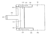
第1実施形態は液晶パネルが2方向取り出し型の場合であり、図1(a)は液晶パネル10にフレキシブル配線板を接続してパネルホルダ30内に収納した状態を示す平面図,図1(b)はその正面図,図1(c)はその右側面図,図1(d)は図1(a)のA−A線断面図で、図2は図1(a)に対応する底面図である。図3は液晶パネル10に接続されるフレキシブル配線板100を示す平面図で、図4は液晶パネル10にフレキシブル配線板100を接続する状態を示す平面図である。
The first embodiment is a case where the liquid crystal panel is a two-way take-out type, and FIG. 1A is a plan view showing a state in which a flexible wiring board is connected to the
図1(a),(d)に示すように、液晶パネル10は図示しない液晶層を挟んで対向的に配置される観察面側の透明電極基板11と反観察面側(裏面側)の透明電極基板12とを備えているが、この場合、裏面側の透明電極基板12側のみにその対向する2辺に端子部12a,12bが設けられている。
As shown in FIGS. 1A and 1D, the
なお、この例においても上記従来例と同じく各端子部12a,12bに表示データ処理用などのチップ部品CHが実装されているが、本発明においてチップ部品CHの有無は任意である。また、図1(d)に示すように液晶パネル10はバックライトに含まれる導光板31とともにパネルホルダ30内に収納されているが、バックライトの有無も任意に選択されてよい。
In this example as well, the chip parts CH for display data processing and the like are mounted on the
図3を参照して、フレキシブル配線板100はマザー的な大判サイズのフレキシブル配線板から打ち抜かれたもので、幹配線板110,第1,第2の枝配線板120,130およびコネクタ用配線板150を一体に備えている。
Referring to FIG. 3,
このうちの幹配線板110は、図2に示すように最終的にパネルホルダ30の底面30a側に配置されることからパネルホルダ30の底面30a内に収まる大きさに形成されている。幹配線板110の例えば点線で仕切られている部分が回路基板部111であり、図示しないが、この回路基板部111に液晶駆動部品やバックライト駆動部品を含む制御回路が設けられる。
Of these, the
第1および第2の枝配線板120,130は各端子部12a,12bに接続される枝配線板で、幹配線板110の両端側から同一方向に引き出されている。枝配線板120,130は左右対称形であるため、その一方の枝配線板120について説明し他方の枝配線板130についてはその参照符号を括弧内に記す。
The first and second
枝配線板120(130)は、図2に示すように幹配線板110とともにパネルホルダ30の底面30aに沿って配置される基端部121(131)と、基端部121(131)から外側に向けてほぼ直角に折り曲げられ図1(c)に示すようにパネルホルダ30の右側面30bに沿って配置される第1屈曲部122(132)と、第1屈曲部122(132)からほぼ直角に折り曲げられ図1(a)に示すように端子部12a(12b)の一部分に沿って配置される第1帯板部123(133)と、第1帯板部123(133)からさらに外側に向けてほぼ直角に折り曲げられ図1(b),図2に示すようにパネルホルダ30の正面側(背面側)の側面30c(30d)から底面30aかけて配置される第2屈曲部124(134)と、第2屈曲部124(134)からほぼ直角に折り曲げられ図2に示すようにパネルホルダ30の底面30aに沿って配置される第2帯板部125(135)と、第2帯板部125(135)から内側に向けてほぼ直角に折り曲げられ図1(a),(b)に示すようにパネルホルダ30の正面側(背面側)の側面30c(30d)から端子部12a(12b)にかけて配置される第3屈曲部126(136)とを備え、第3屈曲部126(136)の先端部に端子部12a(12b)と接続される電極部127(137)が形成されている。
As shown in FIG. 2, the branch wiring board 120 (130) includes a base end part 121 (131) disposed along the
コネクタ用配線板150は幹配線板110のほぼ中央部分から枝配線板120,130と同一方向に引き出されパネルホルダ30の外側にまで延びる長さを備えている。コネクタ用配線板150の先端にはコネクタ電極部151が形成されている。
The
次に、図4を併せて参照して液晶パネル10にフレキシブル配線板100を取り付ける手順の一例について説明する。まず、液晶パネル10をパネルホルダ30に入れる前の段階でフレキシブル配線板100を液晶パネル10に接続する。すなわち、フレキシブル配線板100をフラットな状態として、その枝配線板120,130の各電極部127,137を端子部12a,12bの所定位置に位置決めしたのち、例えば異方性導電フィルムを介して接続する。この接続に伴って第1帯板部123,133が端子部12a,12b上に配置される。
Next, an example of a procedure for attaching the
また、第1帯板部123,133は、端子部12a,12bと電極部127,137との接続を補強するために端子部12a,12b上に固着されていることが好ましい。その固着手段としては、両面粘着テープや異方性導電フィルムでの固着を例示することができる。異方性導電フィルムでの固着は電極部127,137の接続と同じタイミングで行うことができるのでより好ましい。
Moreover, it is preferable that the
接続が完了したら液晶パネル10をパネルホルダ30内に収納し、第2屈曲部124,134および第3屈曲部126,136をパネルホルダ30の側面30c,30dの上端縁に沿って折り曲げ線aのところで山折りし、さらに上記側面30c,30dの下端縁に沿って折り曲げ線bのところで山折りして第2帯板部125,135をパネルホルダ30の底面30aに配置する。
When the connection is completed, the
次に、第1屈曲部122,132をパネルホルダ30の右側面30bの上端縁に沿って折り曲げ線cのところで山折りし、さらに上記右側面30bの下端縁に沿って折り曲げ線dのところで山折りする。これにより、図2に示すように幹配線板110がパネルホルダ30の底面30aに配置されるとともにコネクタ用配線板150がパネルホルダ30の外側に引き出される。なお、上記の各折り曲げ線a〜dは仮想線であるが、あらかじめその部分に折り曲げやすくする加工を施してもよい。
Next, the first
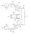
次に、図5ないし図8により本発明の第2実施形態について説明する。この第2実施形態において液晶パネル10は3つの端子部を備える3方向取り出し型である。図5(a)〜(d)は図1(a)〜(d)と、図6は図2と、図7は図3と、図8は図4とそれぞれ対応している。
Next, a second embodiment of the present invention will be described with reference to FIGS. In the second embodiment, the
この第2実施形態で上記第1実施形態と異なる点は、液晶パネル10が3方向取り出し型であり、それに伴ってフレキシブル配線板100に第3の枝配線板140が追加されている点であり、その他の構成については上記第1実施形態と同じであってよいためその説明は省略する。
The second embodiment differs from the first embodiment in that the
図5(a)および図8の平面図に示すように、この第2実施形態において、液晶パネル10は裏面側の透明電極基板12側の3辺の各々に端子部12a,12b,12cを備えている。このうちの端子部12a,12bは上記第1実施形態と同じく対向する2辺に設けられており、端子部12cは残りの2辺のうちのコネクタ用配線板150がパネル外に引き出される側の一方の辺に設けられている。端子部12cにもチップ部品CHが実装されているが、本発明はCOG型に限定されるものでないことは上述したとおりである。
As shown in the plan views of FIGS. 5A and 8, in the second embodiment, the
図7を参照して、この第2実施形態において、フレキシブル配線板100は端子部12a用の第1の枝配線板120,端子部12b用の第2の枝配線板130およびコネクタ用配線板150に加えて端子部12c用の第3の枝配線板140を備えている。
Referring to FIG. 7, in this second embodiment,
第3の枝配線板140は幹配線板110から第1および第2の各枝配線板120,130と同じ方向に引き出され、その先端部には端子部12cと接続される電極部141が形成されている。第3の枝配線板140は第1および第2の枝配線板120,130の間の任意の位置から引き出されてよいが、スペース的には図7に示すようにコネクタ用配線板150と重なる位置に設けられることが好ましい。
The third
すなわち、第3の枝配線板140は端子部12cとの位置関係からして他の枝配線板120,130よりも短くてよいため、コネクタ用配線板150の幹配線板110に対する基端部側にほぼコ字状(門型)の切り込み溝を入れて幹配線板110に連設する切り起こし片を形成し、その切り起こし片に第3の枝配線板140を割り当てることが好ましい。
That is, since the third
図8を参照して、この第2実施形態においても上記第1実施形態と同じくフレキシブル配線板100をフラットな状態として第1ないし第3の枝配線板120,130,140の各電極部127,137,141を端子部12a,12b,12cに接続してパネルホルダ30内に収納する。
Referring to FIG. 8, also in the second embodiment, the
そして、上記第1実施形態で説明したように、第1および第2の枝配線板120,130を上記折り曲げ線a,bに沿って山折りしたのち、上記折り曲げ線c,dに沿って山折りする際に第3の枝配線板140をともに山折りすることにより、図6に示すように幹配線板110がパネルホルダ30の底面30aに配置されるとともにコネクタ用配線板150がパネルホルダ30の外側に引き出される。
Then, as described in the first embodiment, the first and second
上記したように、液晶パネルがその一方の透明電極基板側のみに2つもしくは3つの端子部を備えている2方向取り出し型もしくは3方向取り出し型であるにしても、本発明によれば、それに接続されるフレキシブル配線板は1枚構成でしかもフラットな状態で各端子部に接続することが可能であるため、接続作業を容易に行えるとともに信頼性の高い接続状態を得ることができる。 As described above, even if the liquid crystal panel is a two-way take-out type or a three-way take-out type having only two or three terminal portions on one transparent electrode substrate side, according to the present invention, Since the flexible wiring board to be connected can be connected to each terminal portion in a single-plate configuration and in a flat state, connection work can be easily performed and a highly reliable connection state can be obtained.
なお、本発明は液晶表示装置に限定されるものではなく、有機EL表示装置やプラズマ表示装置などの電気光学表示装置にも適用することができる。 Note that the present invention is not limited to a liquid crystal display device, and can also be applied to an electro-optical display device such as an organic EL display device or a plasma display device.
10 液晶パネル
12a,12b,12c 端子部
30 パネルホルダ
100 フレキシブル配線板
110 幹配線板
120 第1の枝配線板
130 第2の枝配線板
140 第3の枝配線板
150 コネクタ用配線板
DESCRIPTION OF
Claims (4)
上記フレキシブル配線板は上記一方の基板の裏面側に配置される幹配線板と、上記幹配線板の両端側の2箇所から同一方向に向けて引き出され上記各端子部にそれぞれ接続される第1,第2の枝配線板と、上記幹配線板の所定箇所から上記表示パネルの外側に向けて引き出されるコネクタ用配線板とを含み、上記幹配線板,上記各枝配線板および上記コネクタ用配線板が1枚のフレキシブル配線板により一体に形成され、上記第1,第2の枝配線板に含まれている電極部と所定の帯板部とが上記各端子部上にそれぞれ載置されていることを特徴とする電気光学表示装置。 In an electro-optical display device including a display panel having terminal portions on two opposite sides of one of the two substrates, and a flexible wiring board connected to each of the terminal portions,
The flexible wiring board is pulled out in the same direction from a trunk wiring board disposed on the back side of the one substrate and two positions on both ends of the trunk wiring board, and is connected to the terminal portions, respectively. , A second branch wiring board, and a connector wiring board drawn out from a predetermined position of the trunk wiring board toward the outside of the display panel, the trunk wiring board, the branch wiring boards, and the connector wiring The board is integrally formed by one flexible wiring board, and the electrode part and the predetermined strip part included in the first and second branch wiring boards are respectively placed on the terminal parts. An electro-optical display device.
上記フレキシブル配線板は上記一方の基板の裏面側に配置される幹配線板と、上記幹配線板の両端側の2箇所から同一方向に向けて引き出され対向する2辺に設けられている上記各端子部にそれぞれ接続される第1,第2の枝配線板と、上記幹配線板の両端側の2箇所の間の所定の1箇所から上記同一方向に向けて引き出され残りの1辺に設けられている上記端子部に接続される第3の枝配線板と、上記幹配線板の所定箇所から上記表示パネルの外側に向けて引き出されるコネクタ用配線板とを含み、上記幹配線板,上記各枝配線板および上記コネクタ用配線板が1枚のフレキシブル配線板により一体に形成され、上記第1,第2の枝配線板に含まれている電極部と所定の帯板部とが上記各端子部上にそれぞれ載置されていることを特徴とする電気光学表示装置。 In an electro-optic display device including a display panel having terminal portions on three sides of one of the two substrates, and a flexible wiring board connected to each of the terminal portions,
The flexible wiring board is provided on two opposing sides which are drawn out in the same direction from two locations on both ends of the trunk wiring board and the trunk wiring board disposed on the back side of the one substrate. The first and second branch wiring boards respectively connected to the terminal portion and the predetermined one place between the two places on both ends of the trunk wiring board are drawn in the same direction and provided on the remaining one side. A third branch wiring board connected to the terminal portion, and a connector wiring board drawn out from a predetermined portion of the trunk wiring board toward the outside of the display panel, the trunk wiring board, Each branch wiring board and the connector wiring board are integrally formed by a single flexible wiring board, and the electrode portion and the predetermined band plate portion included in the first and second branch wiring boards are each It is characterized by being placed on each terminal part Electro-optical display devices.
Priority Applications (1)
| Application Number | Priority Date | Filing Date | Title |
|---|---|---|---|
| JP2004106019A JP2005292389A (en) | 2004-03-31 | 2004-03-31 | Electrooptical display device |
Applications Claiming Priority (1)
| Application Number | Priority Date | Filing Date | Title |
|---|---|---|---|
| JP2004106019A JP2005292389A (en) | 2004-03-31 | 2004-03-31 | Electrooptical display device |
Publications (1)
| Publication Number | Publication Date |
|---|---|
| JP2005292389A true JP2005292389A (en) | 2005-10-20 |
Family
ID=35325389
Family Applications (1)
| Application Number | Title | Priority Date | Filing Date |
|---|---|---|---|
| JP2004106019A Withdrawn JP2005292389A (en) | 2004-03-31 | 2004-03-31 | Electrooptical display device |
Country Status (1)
| Country | Link |
|---|---|
| JP (1) | JP2005292389A (en) |
Cited By (5)
| Publication number | Priority date | Publication date | Assignee | Title |
|---|---|---|---|---|
| US8269940B2 (en) | 2008-02-04 | 2012-09-18 | Au Optronics Corp. | Sensing structure |
| JP2016014755A (en) * | 2014-07-02 | 2016-01-28 | セイコーエプソン株式会社 | Electro-optic module and electronic equipment |
| WO2016129278A1 (en) * | 2015-02-12 | 2016-08-18 | 古河電気工業株式会社 | Flexible substrate, component with flexible substrate, and method for producing component with flexible substrate |
| CN106163086A (en) * | 2016-06-28 | 2016-11-23 | 广东欧珀移动通信有限公司 | PCB assembly and mobile terminal with same |
| CN106773391A (en) * | 2017-02-14 | 2017-05-31 | 奇纬光电新材料(中国)有限公司 | A kind of wiring construction of light modulation film |
-
2004
- 2004-03-31 JP JP2004106019A patent/JP2005292389A/en not_active Withdrawn
Cited By (8)
| Publication number | Priority date | Publication date | Assignee | Title |
|---|---|---|---|---|
| US8269940B2 (en) | 2008-02-04 | 2012-09-18 | Au Optronics Corp. | Sensing structure |
| JP2016014755A (en) * | 2014-07-02 | 2016-01-28 | セイコーエプソン株式会社 | Electro-optic module and electronic equipment |
| WO2016129278A1 (en) * | 2015-02-12 | 2016-08-18 | 古河電気工業株式会社 | Flexible substrate, component with flexible substrate, and method for producing component with flexible substrate |
| CN107251659A (en) * | 2015-02-12 | 2017-10-13 | 古河电气工业株式会社 | The manufacture method of flexible base board, the part with flexible base board and the part with flexible base board |
| JPWO2016129278A1 (en) * | 2015-02-12 | 2017-11-24 | 古河電気工業株式会社 | Flexible substrate, component with flexible substrate, and method for manufacturing component with flexible substrate |
| US10869395B2 (en) | 2015-02-12 | 2020-12-15 | Furukawa Electric Co., Ltd. | Flexible substrate, flexible substrate-attached component, and manufacturing method of flexible substrate-attached component |
| CN106163086A (en) * | 2016-06-28 | 2016-11-23 | 广东欧珀移动通信有限公司 | PCB assembly and mobile terminal with same |
| CN106773391A (en) * | 2017-02-14 | 2017-05-31 | 奇纬光电新材料(中国)有限公司 | A kind of wiring construction of light modulation film |
Similar Documents
| Publication | Publication Date | Title |
|---|---|---|
| CN103718229B (en) | Display device | |
| CN102007523B (en) | Electronic package, display device, and electronic device | |
| CN101241243B (en) | Device comprising flexible printed circuit and connection auxiliary member and housing on which a circuit board is mounted | |
| CN102809091A (en) | Led backlight and liquid crystal display | |
| KR102600528B1 (en) | Display device | |
| CN102736316A (en) | Liquid crystal display device | |
| US9807880B2 (en) | Circuit board and lighting device having the circuit board | |
| KR102034058B1 (en) | Display device | |
| EP1681910B1 (en) | Connecting device of a flexible printed circuit board | |
| US20140185251A1 (en) | Display device | |
| JP5019604B2 (en) | Liquid crystal display | |
| US20210223622A1 (en) | Display device | |
| CN103732973A (en) | Lighting device and display device provided with same | |
| EP2858465A1 (en) | Circuit board and lighting device having the circuit board | |
| JP2005292389A (en) | Electrooptical display device | |
| JP5170133B2 (en) | Display device | |
| JP2006119321A (en) | Conductive connection structure between electrical circuits | |
| KR20120018677A (en) | Flexible printed circuit board and liquid crystal display panel having flexible printed circuit board | |
| KR20150004173A (en) | Printed circuit board | |
| US9123265B2 (en) | Planer light source device with fixing portion and display device using the same | |
| CN207584390U (en) | Planar illuminating device and substrate | |
| KR102350240B1 (en) | Display device | |
| JP2001091968A (en) | Electro-optical devices and electronic equipment | |
| KR20070036011A (en) | LC module | |
| JP2011186254A (en) | Liquid crystal display device |
Legal Events
| Date | Code | Title | Description |
|---|---|---|---|
| A300 | Withdrawal of application because of no request for examination |
Free format text: JAPANESE INTERMEDIATE CODE: A300 Effective date: 20070605 |