JP2005292380A - Display using coherent light - Google Patents
Display using coherent light Download PDFInfo
- Publication number
- JP2005292380A JP2005292380A JP2004105837A JP2004105837A JP2005292380A JP 2005292380 A JP2005292380 A JP 2005292380A JP 2004105837 A JP2004105837 A JP 2004105837A JP 2004105837 A JP2004105837 A JP 2004105837A JP 2005292380 A JP2005292380 A JP 2005292380A
- Authority
- JP
- Japan
- Prior art keywords
- sub
- scanning
- coherent light
- synchronization signal
- circuit
- Prior art date
- Legal status (The legal status is an assumption and is not a legal conclusion. Google has not performed a legal analysis and makes no representation as to the accuracy of the status listed.)
- Pending
Links
Images
Landscapes
- Mechanical Optical Scanning Systems (AREA)
Abstract
【課題】可動部品を用いることなく、スペックルを低減できるコヒーレント光を用いるディスプレイである。
【解決手段】コヒーレント光を用いるディスプレイは、変調可能なコヒーレント光源105と、コヒーレント光源105から射出されるコヒーレント光を主走査する主走査手段101と、コヒーレント光を主方向とは副走査する副走査手段103と、コヒーレント光源105、主走査手段101、副走査手段103の同期制御を行う同期制御手段107と、同期制御手段107から出力される副走査手段103の副走査同期信号を、副走査手段103の走査周期毎に時間的にシフトさせて、画素での光スポットの副方向の位置を変化させる副走査同期信号シフト手段108を備える。
【選択図】図1A display using coherent light that can reduce speckle without using moving parts.
A display using coherent light includes a coherent light source 105 that can be modulated, main scanning means 101 that performs main scanning of coherent light emitted from the coherent light source 105, and sub scanning that sub-scans the coherent light in the main direction. Means 103, synchronization control means 107 for performing synchronization control of coherent light source 105, main scanning means 101, and sub-scanning means 103; Sub-scanning synchronization signal shifting means 108 is provided for shifting the position of the light spot in the pixel in the sub-direction by shifting it every 103 scanning cycles.
[Selection] Figure 1
Description
本発明はレーザなどのコヒーレント光を用いるディスプレイに関する。 The present invention relates to a display using coherent light such as a laser.
赤、緑、青の3原色のレーザ光を主走査方向(通常は水平方向)、副走査方向(通常は垂直方向)の2つの光偏向器で走査し、画像を形成するレーザディスプレイが知られている。ここで、主走査の方向は走査線の方向であり、通常は水平方向である。そして、副走査の方向は走査線と直交する方向であり、通常は垂直方向である。この2つの走査により2次元の走査領域(すなわち画面)が形成される。レーザ光の持つ指向性と単色性は高解像度・良画質ディスプレイに適している。一方で、レーザ光の干渉性のために画像に微細な光のドットが重畳されているように見える。これはスペックルと呼ばれ、この除去がレーザ走査型ディスプレイの大きな課題である。スペックルは、投影面の各点で散乱されたコヒーレント光が、面の微細な凹凸に起因するランダムな位相関係で干渉しあって生じるものである。 There is known a laser display that forms an image by scanning laser light of three primary colors of red, green, and blue with two optical deflectors in a main scanning direction (usually a horizontal direction) and a sub-scanning direction (usually a vertical direction). ing. Here, the direction of main scanning is the direction of scanning lines, and is usually the horizontal direction. The sub-scanning direction is a direction orthogonal to the scanning line, and is usually the vertical direction. A two-dimensional scanning region (that is, a screen) is formed by these two scans. The directivity and monochromaticity of laser light is suitable for high-resolution and good-quality displays. On the other hand, due to the coherence of the laser light, it appears that fine light dots are superimposed on the image. This is called speckle, and this removal is a major problem for laser scanning displays. Speckle is generated when coherent light scattered at each point on the projection surface interferes with each other in a random phase relationship caused by fine irregularities on the surface.
スペックルの除去方法の一例を説明する。図6は、コヒーレント光を用いる無スペックル・ディスプレイの構成図である(特許文献1参照)。この構成では、赤色レーザ601、青色レーザ602、緑色レーザ603のレーザ光を、ダイクロイック・ビームスプリッタ605〜607で合わせ、集光レンズ609を介して空間光変調器610で変調し、観察面611に投影する。そして、スペックルを無くすために、拡散素子607をコイルまたはモータ608により回転する。これによりスペックルパターンは分裂し、観察面611のスペックルは無くなる。
しかしながら、前記の方式では拡散素子を回転する機構が必須となり、レーザディスプレイの小型化、低消費電力化の点で不利である。 However, the above-described method requires a mechanism for rotating the diffusion element, which is disadvantageous in terms of downsizing the laser display and reducing power consumption.
前述の課題に鑑み、本発明のコヒーレント光を用いるディスプレイは、変調可能なコヒーレント光源と、コヒーレント光源から射出されるコヒーレント光を主走査する主走査手段と、コヒーレント光副走査する副走査手段と、コヒーレント光源、主走査手段、副走査手段の同期制御を行う同期制御手段と、同期制御手段から出力される副走査手段の副走査同期信号を、副走査手段の走査周期毎に時間的にシフトさせて、画素での光スポットの副走査方向の位置を変化させる副走査同期信号シフト手段を備えることを特徴とする。この構成では、投影面などの各点で散乱されるコヒーレント光によるスペックルの模様が人の残像時間内で変化して画素内で平均化され、スペックルを低減することができる。そして、これを、可動機構を用いることなく、副走査同期信号シフト手段という電気的な処理をする手段で行なっている。 In view of the foregoing problems, a display using coherent light according to the present invention includes a coherent light source that can be modulated, a main scanning unit that scans coherent light emitted from the coherent light source, a sub-scanning unit that sub-scans coherent light, The synchronization control means for controlling the synchronization of the coherent light source, the main scanning means, and the sub-scanning means, and the sub-scanning synchronization signal of the sub-scanning means output from the synchronization control means are shifted in time for each scanning period of the sub-scanning means. And a sub-scanning synchronization signal shifting means for changing the position of the light spot in the pixel in the sub-scanning direction. In this configuration, the speckle pattern due to coherent light scattered at each point such as the projection surface changes within the afterimage time of the person and is averaged within the pixel, thereby reducing speckle. This is performed by means of electrical processing called sub-scanning synchronization signal shifting means without using a movable mechanism.
上記構成の本発明により、可動部品を用いることなく、スペックルを低減できる。また、可動部品を用いないので、小型、低消費電力のレーザ走査型ディスプレイなども実現でき、その画質を良くすることができる。 According to the present invention having the above-described configuration, speckle can be reduced without using moving parts. Further, since no moving parts are used, a compact, low power consumption laser scanning display or the like can be realized, and the image quality can be improved.
以下に本発明の一実施形態を説明する。
本実施形態のレーザディスプレイでは、スクリーン上に形成される画素での光スポットの副走査方向の位置をフレーム毎で変えることによりスペックルを低減する。光スポットの位置がフレーム毎に変わることで、スペックルパターンがフレーム毎に変わり、それによりスペックルを低減できる。スクリーン上に形成される画素での光スポットの副走査方向の位置の変更は、副走査の同期信号(副走査同期信号)をフレーム毎にシフトさせることで行う。
An embodiment of the present invention will be described below.
In the laser display of the present embodiment, speckle is reduced by changing the position of the light spot in the sub-scanning direction at each pixel formed on the screen for each frame. By changing the position of the light spot for each frame, the speckle pattern changes for each frame, thereby reducing speckle. The position of the light spot in the pixel formed on the screen is changed by shifting the sub-scanning synchronizing signal (sub-scanning synchronizing signal) for each frame.
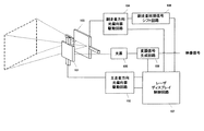
図1は本実施形態のレーザディスプレイの構成図である。このレーザディスプレイは、主走査方向光偏向器101、主走査方向光偏向器駆動回路102、副走査方向光偏向器103、副走査方向光偏向器駆動回路104、レーザ光源105、変調信号生成回路106、レーザディスプレイ制御回路107、副走査同期信号シフト回路108で構成される。図1中には、走査されるレーザ光が点線で示してある。
FIG. 1 is a configuration diagram of a laser display according to the present embodiment. This laser display includes a main scanning direction
この構成において、主走査方向光偏向器101は、レーザ光源105から入射された光ビームを走査し、1次元の走査光を形成する。こうした主走査方向光偏向器101の小型なデバイスとしては、単結晶シリコンを用いた両持ちバネ構造の共振型のものがある。これへの駆動回路102からの駆動波形は正弦波、三角波、矩形波等である。この主走査方向光偏向器101の共振周波数は、レーザディスプレイの走査線数と副走査の非描画期間、画面のフレームレートで決定され、20kHz程度である。主走査方向光偏向器駆動回路102は主走査方向光偏向器101を駆動する。主走査方向光偏向器駆動回路102は、これに入力されるレーザディスプレイ制御回路107からの駆動波形の振幅および同期信号に基づき駆動信号を生成する。
In this configuration, the main scanning direction
副走査方向光偏向器103は、主走査方向光偏向器101から入射される光ビームの走査線を該走査線と垂直方向に副走査し、2次元の走査を行う。この副走査方向光偏向器103には、両持ちバネ構造の共振あるいは非共振型を用いることができる。一般的には非共振で動作され、駆動波形は三角波、鋸波等である。この光偏向器103の駆動周波数はレーザディスプレイのフレームレートで決定される。例えば60Hz程度である。副走査方向光偏向器駆動回路104は副走査方向光偏向器103を駆動する。副走査方向光偏向器駆動回路104は、これに入力される駆動波形の振幅および同期信号に基づき駆動信号を生成する。
The sub-scanning direction
光源105は、半導体レーザ等の直接変調可能な発光素子およびその駆動回路、あるいは固体レーザと外部変調器およびその駆動回路の組み合わせ、およびビーム形成用光学系からなる。例えば、赤、緑、青のレーザを備える。変調信号生成回路106は、レーザディスプレイに外部から入力される映像信号をもとに光源105の変調信号を生成する。変調の同期信号および制御信号はレーザディスプレイ制御回路107から入力される。
The light source 105 includes a light-emitting element that can be directly modulated, such as a semiconductor laser, and its drive circuit, or a combination of a solid-state laser, an external modulator, and its drive circuit, and a beam forming optical system. For example, red, green and blue lasers are provided. The modulation
レーザディスプレイ制御回路107は、主走査方向光偏向器駆動回路102、副走査方向光偏向器駆動回路104、変調信号生成回路106、副走査同期信号シフト回路108と接続される。レーザディスプレイ制御回路107は、主走査方向光偏向器駆動回路102および副走査方向光偏向器駆動回路105の振幅設定入力信号を出力するとともに、主走査方向光偏向器駆動回路102には水平走査の同期信号を出力し、副走査同期信号シフト回路108には副走査の同期信号を出力する。副走査同期信号シフト回路108は、レーザディスプレイ制御回路107から入力される副走査同期信号をシフトした信号を生成し、これを副走査方向光偏向器駆動回路104に出力する。そのシフト量については後述する。
The laser
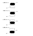
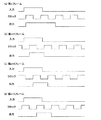
図2は、本実施形態でのレーザディスプレイの画素内での光スポットの位置を示す模式図である。或る画素内での光スポットの位置の変化を、(a)第nフレーム、(b)第n+1フレーム、(c)第n+2フレーム、(d)第n+3フレームの4つのフレームについて示している。図中、画素の符号は201〜204、光スポットの符号は211〜214である。 FIG. 2 is a schematic diagram showing the position of the light spot in the pixel of the laser display in this embodiment. The change of the position of the light spot in a certain pixel is divided into four (a) nth frame, (b) n + 1th frame, (c) n + 2 frame, (d) n + 3 frame. Shows the frame. In the figure, reference numerals of pixels are 201 to 204, and reference numerals of light spots are 211 to 214.
ここで、レーザディスプレイのスクリーンでの画素と走査される光スポットの関係について説明する。レーザディスプレイでは、光スポットは画素時間分、主走査方向に移動する。そのため光スポットは主走査方向に長くなる。スクリーン上での光スポットの大きさは主走査方向光偏向器101のミラーサイズに反比例する。主走査方向光偏向器101のミラーの主走査方向のサイズと副走査方向のサイズが同じ場合、光スポットの主走査方向のサイズと副走査方向のサイズは同じになる。前述の主走査による光スポットの広がりを考慮し、光スポットを画素より小さくすると、副走査方向の光スポットは図2で示すように、画素より小さくなる。本発明ではこのことを利用して、画素の副走査方向での光スポットの位置をフレーム毎に変化させる(部分的に重なっていてもよい)。
Here, the relationship between the pixels on the screen of the laser display and the scanned light spot will be described. In the laser display, the light spot moves in the main scanning direction by the pixel time. Therefore, the light spot becomes longer in the main scanning direction. The size of the light spot on the screen is inversely proportional to the mirror size of the
画素の副走査方向での光スポットの位置を変えるために、副走査同期信号シフト回路108により、副走査同期信号をフレーム単位でシフトさせる。図2では4フレームを1周期として画素の副走査方向での光スポットの位置を変えている。第nフレームと第n+4フレームでは同じ位置に来る。尚、この周期は一例であり、数は別の値でもよい。また、副走査方向での光スポットの位置のシフトが、1画素の範囲内で、人間の目の残像時間以下でほぼ平均的に行われていれば(すなわち、光照射量がほぼ平均的になっていれば)、必ずしも固定の周期性を持つ必要はない(後述の実施例1では固定の周期性を持つが、実施例2では周期性を持たない)。また、周期内でのシフト量の変化は単調である必要はない。例えば、図2で第n+1フレームでの光スポットの位置と第n+3フレームでの光スポットの位置が逆になっていてもよい。
In order to change the position of the light spot in the sub-scanning direction of the pixel, the sub-scanning synchronization
本実施形態により、各画素での光スポットの副走査方向の位置を変化させることで、投影面の各点で散乱されるコヒーレント光によるスペックルの模様が人の残像時間内で変化して、画素内で平均化されスペックルを低減できる。そして、可動部品を用いることなくスペックルを低減している。 According to this embodiment, by changing the position of the light spot in each pixel in the sub-scanning direction, the speckle pattern due to the coherent light scattered at each point on the projection surface changes within the afterimage time of the person, Speckle can be reduced by averaging within the pixel. And speckle is reduced without using movable parts.
以下、より具体的な実施例を挙げて本発明を説明する。
(実施例1)
実施例1では、副走査同期信号シフト手段ないし回路108が、遅延時間が異なる複数の遅延手段と、複数の遅延手段の信号を選択する選択手段と、第2走査同期信号を計数しその値に対応して選択手段による前記信号選択を制御する計数手段とで構成される。本実施例の特徴は、レーザディスプレイの制御系が1つの動作クロックで動いており、画素の副走査方向での光スポットの位置のフレーム毎のシフトを動作クロックに同期して行うことである。以下の例ではシフト量が4フレームで一巡する(図2と同じ)。
Hereinafter, the present invention will be described with reference to more specific examples.
(Example 1)
In the first embodiment, the sub-scanning synchronization signal shifting unit or
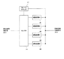
図3は、副走査同期信号シフト回路の実施例1の構成図である。副走査同期信号シフト回路108は、遅延回路A301、遅延回路B302、遅延回路C303、遅延回路D304、フレームカウンタ311、セレクタ312で構成される。
FIG. 3 is a configuration diagram of Embodiment 1 of the sub-scanning synchronization signal shift circuit. The sub-scanning synchronization
遅延回路A301、遅延回路B302、遅延回路C303、遅延回路D304には副走査同期信号がレーザディスプレイ制御回路107から入力される。遅延回路各々に固定の遅延量が設定されており、その遅延分、入力される副走査同期信号を遅延、つまり時間的にシフトさせる。フレームカウンタ311は、入力される副走査同期信号をカウントし、そのカウント数に応じてセレクタ312を制御する。カウンタ311は4でリセットされる。従って、セレクタ312の制御状態は“0”、“1”、“2”、“3”の4つである。セレクタ312は、フレームカウンタ311からの制御信号に応じて、接続する入力(接続する遅延回路)を選択する。セレクタ312の制御状態“0”で遅延回路A301を選択し、セレクタ312の制御状態“1”で遅延回路B302を選択し、セレクタ312の制御状態“2”で遅延回路C303を選択し、セレクタ312の制御状態“3”で遅延回路D304を選択する。これにより、セレクタ312からは、選択した遅延回路の遅延量に対応した副走査同期信号が出力される。
A sub-scanning synchronization signal is input from the laser
ここで、各遅延回路の遅延量について説明する。垂直方向(副走査方向)で隣接する画素の描画時間間隔は主走査の周期である。この周期をThとすると、各遅延回路の遅延量は、
遅延回路A301:0、
遅延回路B302:0.2Th
遅延回路C303:0.4Th
遅延回路D304:0.6Th
となる。尚、遅延量をThに対して4等分ではなく5等分(0.2Thずつ)にしているのは、光スポットを画素内に収めるためである。
Here, the delay amount of each delay circuit will be described. The drawing time interval between adjacent pixels in the vertical direction (sub-scanning direction) is the period of main scanning. When this period is Th, the delay amount of each delay circuit is
Delay circuit A301: 0,
Delay circuit B302: 0.2 Th
Delay circuit C303: 0.4 Th
Delay circuit D304: 0.6 Th
It becomes. The reason for setting the delay amount to 5 equal parts (by 0.2 Th) rather than 4 equal parts to Th is to keep the light spot in the pixel.
本実施例では、レーザディスプレイの制御系の動作クロックを基準に、画素内での光スポットの副走査位置のシフトを周期的(決定した通りに)に制御するため、方式のシステム設計が容易である。 In this embodiment, since the shift of the sub-scanning position of the light spot in the pixel is controlled periodically (as determined) based on the operation clock of the control system of the laser display, the system design of the system is easy. is there.
(実施例2)
実施例2では、副走査同期信号シフト手段ないし回路108が、レーザディスプレイの制御回路107の動作クロックと独立したクロック(副走査方向光偏向器駆動回路104の制御系の動作クロック)を発生するクロック発生手段と、該独立したクロックの入力状態に応じて出力信号を入力信号と一致させその後保持する論理回路手段を備え、論理回路手段に副走査同期信号を該入力信号として入力することを特徴とする。従って、本実施例では、画素内での光スポットの副走査方向の位置のフレーム毎のシフト量が固定でない。
(Example 2)
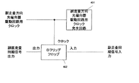
In the second embodiment, the sub-scanning synchronization signal shifting means or
図4は、実施例2の副走査同期信号シフト回路108の構成図である。このシフト回路108は、副走査方向光偏向器駆動回路用クロック発生回路401とDフリップフロップ402で構成される。副走査方向光偏向器駆動回路用クロック発生回路401は、副走査方向光偏向器駆動回路104の動作クロックを生成する。このクロックの周期は、レーザディスプレイの他の制御系の動作クロック(レーザディスプレイ制御回路107の動作クロック)の周期より長く設定されている。Dフリップフロップ402は、レーザディスプレイ制御回路107の動作クロックから生成される副走査同期信号の入力信号をクロック発生回路401からのクロックの立ち上りエッジで出力する。
FIG. 4 is a configuration diagram of the sub-scanning synchronization
図5は、Dフリップフロップ402の信号のタイミングチャートである。入力、クロック、出力の3信号を第nから第n+3フレームについて示している。この図では、シフト量が4フレームで一巡する例を示している。副走査方向光偏向器駆動用クロックは、レーザディスプレイの他の制御系のシステムクロック(レーザディスプレイ制御回路107の動作クロック)と非同期であるため、タイミングがずれていく。図5中では、レーザディスプレイの制御系の動作クロックから生成されている副走査同期信号を基準に記載しているため、副走査光偏向器駆動回路用クロックは各フレームでタイミングがずれている。Dフィリップフロップ402は、副走査光偏向器駆動回路用クロックの立ち上りで出力信号を入力信号に一致させ、その後、次の副走査光偏向器駆動回路用クロックの立ち上りまで保持する。そのため、Dフリップフロップ402からの出力と入力にはズレが生じる。このズレにより、Dフリップフロップ402の入出力間には遅延時間が変化する。この変化により、フレーム毎での副走査同期信号のシフトをランダムで行う。この場合でも、副走査方向での光スポットの位置のシフトが、1画素の範囲内で、人間の目の残像時間以下でほぼ平均的に行われる。
FIG. 5 is a timing chart of signals of the D flip-
本実施例では、シフト数分の遅延回路が不要になる。副走査方向光偏向器駆動回路の動作クロックが装置内の他の駆動/制御系の動作クロックと独立している場合には、本方式を適用するための回路規模を小さくすることができる。 In this embodiment, delay circuits for the number of shifts are not necessary. When the operation clock of the sub-scanning direction optical deflector drive circuit is independent of the operation clocks of other drive / control systems in the apparatus, the circuit scale for applying this method can be reduced.
101:主走査方向光偏向器(第1走査手段)
102:主走査方向光偏向器駆動回路
103:副走査方向光偏向器(第2走査手段)
104:副走査光偏向器駆動回路
105:光源(コヒーレント光源)
107:レーザディスプレイ制御回路(同期制御手段)
108:副走査同期信号シフト回路(第2走査同期信号シフト手段)
101: Main scanning direction optical deflector (first scanning means)
102: Main scanning direction optical deflector drive circuit
103: Sub-scanning direction optical deflector (second scanning means)
104: Sub-scanning light deflector drive circuit
105: Light source (coherent light source)
107: Laser display control circuit (synchronous control means)
108: Sub-scanning synchronization signal shift circuit (second scanning synchronization signal shift means)
Claims (3)
Priority Applications (1)
| Application Number | Priority Date | Filing Date | Title |
|---|---|---|---|
| JP2004105837A JP2005292380A (en) | 2004-03-31 | 2004-03-31 | Display using coherent light |
Applications Claiming Priority (1)
| Application Number | Priority Date | Filing Date | Title |
|---|---|---|---|
| JP2004105837A JP2005292380A (en) | 2004-03-31 | 2004-03-31 | Display using coherent light |
Publications (1)
| Publication Number | Publication Date |
|---|---|
| JP2005292380A true JP2005292380A (en) | 2005-10-20 |
Family
ID=35325383
Family Applications (1)
| Application Number | Title | Priority Date | Filing Date |
|---|---|---|---|
| JP2004105837A Pending JP2005292380A (en) | 2004-03-31 | 2004-03-31 | Display using coherent light |
Country Status (1)
| Country | Link |
|---|---|
| JP (1) | JP2005292380A (en) |
Cited By (4)
| Publication number | Priority date | Publication date | Assignee | Title |
|---|---|---|---|---|
| WO2009116453A1 (en) * | 2008-03-19 | 2009-09-24 | シャープ株式会社 | Camera system, device for driving voice coil motor, and method for driving voice coil motor |
| WO2013100066A1 (en) * | 2011-12-28 | 2013-07-04 | 株式会社Jvcケンウッド | Image display device, control method for image display device, and information output device |
| JP2013530418A (en) * | 2010-04-28 | 2013-07-25 | レモプティックス ソシエテ アノニム | Microprojection device with anti-speckle imaging mode |
| JP2016105176A (en) * | 2015-12-22 | 2016-06-09 | 船井電機株式会社 | Image display device |
-
2004
- 2004-03-31 JP JP2004105837A patent/JP2005292380A/en active Pending
Cited By (5)
| Publication number | Priority date | Publication date | Assignee | Title |
|---|---|---|---|---|
| WO2009116453A1 (en) * | 2008-03-19 | 2009-09-24 | シャープ株式会社 | Camera system, device for driving voice coil motor, and method for driving voice coil motor |
| JP2013530418A (en) * | 2010-04-28 | 2013-07-25 | レモプティックス ソシエテ アノニム | Microprojection device with anti-speckle imaging mode |
| US8998424B2 (en) | 2010-04-28 | 2015-04-07 | Lemoptix Sa | Micro-projection device with anti-speckle imaging mode |
| WO2013100066A1 (en) * | 2011-12-28 | 2013-07-04 | 株式会社Jvcケンウッド | Image display device, control method for image display device, and information output device |
| JP2016105176A (en) * | 2015-12-22 | 2016-06-09 | 船井電機株式会社 | Image display device |
Similar Documents
| Publication | Publication Date | Title |
|---|---|---|
| CN105759443B (en) | Image display device | |
| US8416501B2 (en) | Image display apparatus and method of controlling the same | |
| US20190236762A1 (en) | Device and Method for Projecting an Image | |
| EP3383032B1 (en) | Mems laser scanning projector and method for projecting an image with a mems laser scanning projector | |
| US20100020291A1 (en) | 2-dimensional image display device, illumination light source and exposure illumination device | |
| JP5673544B2 (en) | Laser projection device | |
| US9075246B2 (en) | Image display device having laser light scanning with a variation in scanning speed | |
| US20080204667A1 (en) | Projection display and lighting unit | |
| JP2003279889A (en) | Laser projection display system | |
| EP1720057A1 (en) | Illuminating light source and two-dimensional image display using same | |
| US7986340B2 (en) | Arrangement for and method of projecting a color image by switching scan directions in alternate frames | |
| JP4840175B2 (en) | Image display device | |
| JPWO2012111698A1 (en) | Scanning image display apparatus and image display method thereof | |
| JP2013530418A (en) | Microprojection device with anti-speckle imaging mode | |
| JP6118913B2 (en) | Display device | |
| WO2019044537A1 (en) | Image projection control device, image projection control method, program, and image projection device | |
| JP5609370B2 (en) | Image display device | |
| JP4820025B2 (en) | Optical scanning image display device and image display method thereof | |
| JP2005292380A (en) | Display using coherent light | |
| JP6295967B2 (en) | Drawing apparatus and drawing method | |
| JP2013117575A (en) | Stereoscopic image display device | |
| JP4751545B2 (en) | Optical scanning image display device | |
| JP5863998B2 (en) | Image display device | |
| JP6123877B2 (en) | Image display device | |
| JP2015129784A (en) | Projection type display device |