JP2005292365A - Waveguide type optical multiplexer / demultiplexer - Google Patents
Waveguide type optical multiplexer / demultiplexer Download PDFInfo
- Publication number
- JP2005292365A JP2005292365A JP2004105607A JP2004105607A JP2005292365A JP 2005292365 A JP2005292365 A JP 2005292365A JP 2004105607 A JP2004105607 A JP 2004105607A JP 2004105607 A JP2004105607 A JP 2004105607A JP 2005292365 A JP2005292365 A JP 2005292365A
- Authority
- JP
- Japan
- Prior art keywords
- waveguide
- type optical
- input
- output
- groove
- Prior art date
- Legal status (The legal status is an assumption and is not a legal conclusion. Google has not performed a legal analysis and makes no representation as to the accuracy of the status listed.)
- Pending
Links
- 230000003287 optical effect Effects 0.000 title claims abstract description 150
- 239000000758 substrate Substances 0.000 claims abstract description 15
- 239000011162 core material Substances 0.000 claims description 9
- 229910052751 metal Inorganic materials 0.000 claims description 8
- 239000002184 metal Substances 0.000 claims description 8
- 229920002050 silicone resin Polymers 0.000 claims description 5
- 239000012780 transparent material Substances 0.000 claims description 4
- 230000005540 biological transmission Effects 0.000 description 7
- 238000004519 manufacturing process Methods 0.000 description 3
- 229910052709 silver Inorganic materials 0.000 description 3
- 239000004332 silver Substances 0.000 description 3
- 238000010586 diagram Methods 0.000 description 2
- 230000015572 biosynthetic process Effects 0.000 description 1
- 239000000470 constituent Substances 0.000 description 1
- 230000000694 effects Effects 0.000 description 1
- 239000000463 material Substances 0.000 description 1
Images


Landscapes
- Optical Integrated Circuits (AREA)
Abstract
Description
本発明は、導波路型光合分波器に関するものである。 The present invention relates to a waveguide type optical multiplexer / demultiplexer.
従来光通信に用いられる導波路型光合分波回路は、様々な波長成分を含んだ光を波長成分毎に分け出力する機能を有している(例えば、特許文献1参照)。 2. Description of the Related Art A waveguide-type optical multiplexing / demultiplexing circuit used for conventional optical communication has a function of dividing and outputting light including various wavelength components for each wavelength component (see, for example, Patent Document 1).
図2は、従来の典型的なAWG(Arrayed Waveguide grating)により形成された導波路型光合分波回路を示す。 FIG. 2 shows a waveguide type optical multiplexing / demultiplexing circuit formed by a conventional typical AWG (Arrayed Waveguide Grating).
導波路型光合分波回路10は、光信号を入力するための入力導波路11と、入力導波路11に接続された入力側のスラブ導波路12と、出力導波路15に接続された出力側のスラブ導波路14と、スラブ導波路12、14の間に接続されたアレイ導波路13と、スラブ導波路14からの光信号を出力するためにスラブ導波路14に接続された出力導波路15とによって基板16上に構成されている。
The waveguide type optical multiplexing /
入力導波路11から入射された各波長成分を含んだ光は入力側スラブ導波路12で拡大されてアレイ導波路13へ入射され、アレイ導波路13で位相が調整された後、出力側スラブ導波路14で波長毎にそれぞれ異なる出力導波路15へ集光され、出力導波路15から出力される。
The light including each wavelength component incident from the
従来、導波路型光合分波回路の歩留まりを向上させるため、図3に示すように1つの基板26上に2つの導波路型光合分波回路CA、CBを線対称に配置していた。
Conventionally, in order to improve the yield of the waveguide-type optical multiplexing / demultiplexing circuit, two waveguide-type optical multiplexing / demultiplexing circuits CA and CB are arranged symmetrically on one
これら2つの導波路型光合分波回路CA、CBは、各々が図2に示す導波路型光合分波回路10と同様の構造、構成となっている。
Each of these two waveguide-type optical multiplexing / demultiplexing circuits CA and CB has the same structure and configuration as the waveguide-type optical multiplexing /
すなわち、導波路型光合分波回路CAは、光信号を入力するための入力導波路21aと、入力導波路21aに接続された入力側のスラブ導波路22aと、出力導波路25aに接続された出力側のスラブ導波路24aと、スラブ導波路22a、24aの間に接続されたアレイ導波路23aと、スラブ導波路24aからの光信号を出力するためにスラブ導波路24aに接続された出力導波路25aとによって基板26上に構成されている。
That is, the waveguide type optical multiplexing / demultiplexing circuit CA is connected to an
導波路型光合分波回路CBは、光信号を入力するための入力導波路21bと、入力導波路21bに接続された入力側のスラブ導波路22bと、出力導波路25bに接続された出力側のスラブ導波路24bと、スラブ導波路22b、24bの間に接続されたアレイ導波路23bと、スラブ導波路24bからの光信号を出力するためにスラブ導波路24bに接続された出力導波路25bとによって基板26上に構成されている。
The waveguide type optical multiplexing / demultiplexing circuit CB includes an input waveguide 21b for inputting an optical signal, an input-
このように形成された導波路型光合分波回路10(図2参照)は、例えば1つの導波路型光合分波回路10の歩留まりが50%の場合、図2のように1つの基板16に導波路型光合分波回路10を1回路のみ形成した場合には歩留まりが50%である。これに対して、図3のように1つの基板26に導波路型光合分波回路CA、CBを2回路を形成した場合にはいずれかの回路が使用可能な歩留まりが75%となり、歩留まりを向上させることが可能となっている。
The waveguide type optical multiplexing / demultiplexing circuit 10 (see FIG. 2) formed in this way is formed on one
しかしながら、回路歩留まりが50%を切るような製作の難しい導波路型光合分波回路の場合、1つの基板に2つの回路を収納させる従来の歩留まり改善策では、まだ充分とは言えない。 However, in the case of a waveguide-type optical multiplexing / demultiplexing circuit that is difficult to manufacture such that the circuit yield is less than 50%, the conventional yield improvement measures in which two circuits are accommodated on one substrate are still not sufficient.
導波路型光合分波回路の製造効率を向上させ、製造コストを低減させるために、より高い歩留まり向上策が必要であるという問題がある。 In order to improve the manufacturing efficiency of the waveguide type optical multiplexing / demultiplexing circuit and reduce the manufacturing cost, there is a problem that a higher yield improvement measure is required.
また、従来の導波路型光合分波器は使用する光回路の機能を選択することができないという問題がある。 Further, the conventional waveguide type optical multiplexer / demultiplexer has a problem that the function of the optical circuit to be used cannot be selected.
そこで、本発明の目的は、使用する光回路の機能を選択できる光合分波回路を歩留まり良く形成することのできる導波路型光合分波器を提供することにある。 SUMMARY OF THE INVENTION An object of the present invention is to provide a waveguide type optical multiplexer / demultiplexer capable of forming an optical multiplexing / demultiplexing circuit capable of selecting the function of an optical circuit to be used with high yield.
本発明は上記目的を達成するために創案されたものであり、第1の発明は、同一基板上にスラブ導波路を含んだ2つの光合分波回路が互いに交差して形成され、上記交差部分の少なくとも一箇所に溝が設けられている導波路型光合分波器である。 The present invention was devised to achieve the above object, and the first invention is such that two optical multiplexing / demultiplexing circuits including slab waveguides are formed on the same substrate so as to intersect each other, and This is a waveguide type optical multiplexer / demultiplexer in which a groove is provided in at least one place.
第2の発明は、2つの上記導波路型光合分波回路が線対称に配置されているものである。 In the second invention, the two waveguide-type optical multiplexing / demultiplexing circuits are arranged in line symmetry.
第3の発明は、上記溝には、空気が封入されているものである。 In the third invention, air is sealed in the groove.
第4の発明は、上記溝の内壁面には、光を反射する金属からなる金属層が形成されているものである。 In a fourth aspect of the present invention, a metal layer made of a metal that reflects light is formed on the inner wall surface of the groove.
第5の発明は、上記溝には、上記各導波路を形成するコア材との屈折率差の小さなシリコーン樹脂等の透明材質が封入されているものである。 In a fifth aspect of the present invention, a transparent material such as a silicone resin having a small difference in refractive index from the core material forming each waveguide is enclosed in the groove.
本発明によれば、使用する光回路の機能を選択できる光合分波回路を歩留まり良く形成することのできる導波路型光合分波器を得られる。 According to the present invention, it is possible to obtain a waveguide type optical multiplexer / demultiplexer capable of forming an optical multiplexing / demultiplexing circuit capable of selecting the function of an optical circuit to be used with high yield.
以下、本発明の好適実施の形態を添付図面にしたがって説明する。 DESCRIPTION OF EXEMPLARY EMBODIMENTS Hereinafter, preferred embodiments of the invention will be described with reference to the accompanying drawings.
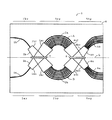
図1は、本発明の実施の形態の一例である導波路型光合分波器を示す。 FIG. 1 shows a waveguide type optical multiplexer / demultiplexer as an example of an embodiment of the present invention.
図示したように導波路型光合分波器1は、同一の基板6上に2系統の導波路型光合分波回路A、Bが形成された光合分波器となっている。
As shown, the waveguide type optical multiplexer /
これらの導波路型光合分波回路A、Bの各構成部位は、屈折率が高く入力された光信号が伝搬する図示しないコア部分と、コア部分よりも屈折率が低くコア部分の周囲を覆っている図示しないクラッド部分とからなる導波路型の光部品である。 Each of the components of the waveguide-type optical multiplexing / demultiplexing circuits A and B covers a core portion (not shown) through which an input optical signal propagates with a high refractive index, and covers the periphery of the core portion with a refractive index lower than that of the core portion. It is a waveguide type optical component comprising a clad portion (not shown).
導波路型光合分波回路Aは、光信号が入力される入力導波路1aと、入力導波路1aに接続された入力側スラブ導波路2aと、入力側スラブ導波路2aに接続され光の波長を調整するアレイ導波路3aと、アレイ導波路3aに接続された出力側スラブ導波路4aと、入力された光信号を出力するための出力導波路5aと備えて構成される。
The waveguide type optical multiplexing / demultiplexing circuit A includes an input waveguide 1a to which an optical signal is input, an input side slab waveguide 2a connected to the input waveguide 1a, and a wavelength of light connected to the input side slab waveguide 2a. Are arranged, an output side slab waveguide 4a connected to the
入力導波路1aは、波長分割多重光信号を導波路型光合分波回路Aに入力する1本以上の導波路から成る光部品である。入力導波路1aに入力された波長分割多重光信号は、接続されている入力側スラブ導波路2aに供給される。 The input waveguide 1a is an optical component composed of one or more waveguides for inputting a wavelength division multiplexed optical signal to the waveguide type optical multiplexing / demultiplexing circuit A. The wavelength division multiplexed optical signal input to the input waveguide 1a is supplied to the connected input slab waveguide 2a.
入力側スラブ導波路2aは、扇型をした導波路型の光部品であり、後述する導波路型光合分波回路Bの入力側スラブ導波路2bと交差して配置されている。入力側スラブ導波路2aは、入力側スラブ導波路2bと交差した部分に光信号を反射若しくは透過するための溝7が設けられた構造となっている。
The input-side slab waveguide 2a is a fan-shaped waveguide-type optical component, and is disposed so as to intersect with an input-
入力側スラブ導波路2aは、入力側スラブ導波路の入力部2ai及び入力側スラブ導波路の出力部2aoに各々1本以上の導波路が設けられた構造となっている。 The input-side slab waveguide 2a has a structure in which one or more waveguides are provided in each of the input section 2ai of the input-side slab waveguide and the output section 2ao of the input-side slab waveguide.
入力側スラブ導波路2aは、入力側スラブ導波路の入力部2aiを入力導波路1aの出力側に接続され、入力側スラブ導波路の出力部2aoをアレイ導波路3aの入力側に接続されている。
The input side slab waveguide 2a has an input part 2ai of the input side slab waveguide connected to the output side of the input waveguide 1a, and an output part 2ao of the input side slab waveguide connected to the input side of the
入力側スラブ導波路2aは、入力導波路1aから供給された波長分割多重光信号を拡大し、設けられている複数のアレイ導波路3aに入射させる機能を有している。
The input-side slab waveguide 2a has a function of expanding the wavelength division multiplexed optical signal supplied from the input waveguide 1a and causing it to enter a plurality of arrayed
アレイ導波路3aは、入力側スラブ導波路2aに接続され、複数本の導波路を有している。アレイ導波路3aの複数本の導波路は、各々の導波路が一定の導波路長差を有しており、入力された光信号の位相を調整することができる。
The
アレイ導波路3aは、位相調整をした光信号を接続されている出力側スラブ導波路4aに供給する。
The
出力側スラブ導波路4aは、扇型をした導波路型の光部品であり、後述する導波路型光合分波回路Bの出力側スラブ導波路4bと交差して配置されている。出力側スラブ導波路4aは、出力側スラブ導波路4bと交差した部分に光信号を反射若しくは透過するための溝8が設けられた構造となっている。
The output-side slab waveguide 4a is a fan-shaped waveguide-type optical component, and is arranged so as to intersect with an output-
出力側スラブ導波路4aは、出力側スラブ導波路の入力部4ai及び出力側スラブ導波路の出力部4aoに各々1本以上の導波路が設けられた構造となっており、入力された光信号の波長毎に集光(分岐)する機能を有している。 The output-side slab waveguide 4a has a structure in which one or more waveguides are provided in the input section 4ai of the output-side slab waveguide and the output section 4ao of the output-side slab waveguide, respectively, and an input optical signal Has a function of condensing (branching) for each wavelength.
出力側スラブ導波路4aは、出力側スラブ導波路の入力部4aiをアレイ導波路3aの出力側に接続され、出力側スラブ導波路の出力部4aoを出力導波路5aの入力側に接続されている。
The output side slab waveguide 4a has an input side 4ai of the output side slab waveguide connected to the output side of the
出力側スラブ導波路4aは、アレイ導波路3aの複数本の導波路から供給された光信号を波長毎にそれぞれ異なる導波路に集光し、集光した各光信号を出力導波路5aへ出力する。
The output-side slab waveguide 4a condenses the optical signals supplied from the plurality of waveguides of the
出力導波路5aは、出力側スラブ導波路4aに接続されており、出力側スラブ導波路4aにより波長毎に集光された光信号を出力する1本以上の導波路から成る光部品である。
The
すなわち出力導波路5aは、入力側スラブ導波路2a、アレイ導波路3a、出力側スラブ導波路4aを順に介して合分波された波長分割多重光信号を導波路型光合分波回路Aから外部に出力するための部位である。
In other words, the
導波路型光合分波回路Bは、光信号が入力される入力導波路1bと、入力導波路1bに接続された入力側スラブ導波路2bと、入力側スラブ導波路2bに接続され光の波長を調整するアレイ導波路3bと、アレイ導波路3bに接続された出力側スラブ導波路4bと、入力された光信号を出力するための出力導波路5bと備えて構成される。
The waveguide type optical multiplexing / demultiplexing circuit B includes an
2系統の導波路型光合分波回路A、Bは、互いに線対称に形成され同様の構成、構造となっているので、導波路型光合分波回路Bの構成部位である入力導波路1b、入力側スラブ導波路2b、アレイ導波路3b、出力側スラブ導波路4b、出力側スラブ導波路の入力部4ai、出力側スラブ導波路の出力部4ao、出力導波路5bの各々の説明は省略する。
Since the two types of waveguide type optical multiplexing / demultiplexing circuits A and B are formed symmetrically with each other and have the same configuration and structure, the
2系統の導波路型光合分波回路A、Bには、入力側スラブ導波路2a、2bの交差した部分に設けられた溝7と、出力側スラブ導波路4a、4bの交差した部分に設けられた溝8とがあり、この溝7、8により分断された構造となっている。
In the two types of waveguide type optical multiplexing / demultiplexing circuits A and B, the groove 7 provided at the intersecting portion of the input
この交差した部分では、各導波路型光合分波回路A、Bを形成している導波路のコア部分が交差する構造となっている。 The intersecting portion has a structure in which the core portions of the waveguides forming the respective waveguide type optical multiplexing / demultiplexing circuits A and B intersect.
本実施の形態の導波路型光合分波器1を形成する導波路型光合分波回路Aには、導波路型光合分波回路Bとの交差部分が溝7によって分断されることにより、入力導波路1aと、溝7よりも入力側にあるスラブ導波路の入力部2aiの部分とから成る入力部1ayが形成されている。
In the waveguide-type optical multiplexer / demultiplexer circuit A forming the waveguide-type optical multiplexer /
また導波路型光合分波回路Aには、入力側スラブ導波路の入力部2aiを除く他の部分である入力側スラブ導波路の出力部2aoと、アレイ導波路3aと、アレイ導波路3aに接続され溝8までの部分である出力側スラブ導波路の入力部4aiとから成るアレイ部3ayが形成されている。
The waveguide-type optical multiplexing / demultiplexing circuit A includes an input-side slab waveguide output section 2ao that is other than the input-side slab waveguide input section 2ai, an
さらに導波路型光合分波回路Aには、導波路型光合分波回路Bとの交差部分が溝8によって分断されることにより、溝8から出力導波路5aに接続された他の部分である出力側スラブ導波路の出力部4aoと、出力側スラブ導波路の出力部4aoに接続された出力導波路5aとから成る出力部5ayが形成されている。
Further, the waveguide type optical multiplexing / demultiplexing circuit A is another part connected to the
同様に導波路型光合分波回路Bには、導波路型光合分波回路Aとの交差部分が溝7によって分断されることにより、入力導波路1bと、溝7よりも入力側にあるスラブ導波路の入力部2biの部分とから成る入力部1byが形成されている。
Similarly, in the waveguide type optical multiplexing / demultiplexing circuit B, the intersection portion with the waveguide type optical multiplexing / demultiplexing circuit A is divided by the groove 7, so that the
また導波路型光合分波回路Bには、入力側スラブ導波路の入力部2biを除く他の部分である入力側スラブ導波路の出力部2boと、アレイ導波路3bと、アレイ導波路3bに接続され溝8までの部分である出力側スラブ導波路の入力部4biとから成るアレイ部3byが形成されている。 The waveguide-type optical multiplexing / demultiplexing circuit B includes an output side 2bo of the input side slab waveguide other than the input part 2bi of the input side slab waveguide, an arrayed waveguide 3b, and an arrayed waveguide 3b. An array part 3by is formed which is connected to the input part 4bi of the output side slab waveguide which is a part up to the groove 8.
さらに導波路型光合分波回路Bには、導波路型光合分波回路Aとの交差部分が溝8によって分断されることにより、溝8から出力導波路5bに接続された他の部分である出力側スラブ導波路の出力部4boと、出力側スラブ導波路の出力部4boに接続された出力導波路5bとから成る出力部5byが形成されている。
Further, the waveguide type optical multiplexing / demultiplexing circuit B is another part connected to the
入力部1ay、1by、アレイ部3ay、3by、出力部5ay、5byの各部は、図示した軸Lに対して例えば上下対称に配置されている。 Each of the input units 1ay and 1by, the array units 3ay and 3by, and the output units 5ay and 5by are arranged, for example, symmetrically with respect to the illustrated axis L.
溝7、8は、決まった形状のものが最初から形成されていて、その溝を透過溝として作用させるか反射溝として作用させるかは、導波路型光合分波器1を評価してから決定する。透過溝として作用させる場合にはシリコーン樹脂などコアと屈折率の近い材料を溝に封入し、反射溝として作用させる場合には溝7、8の内壁面に銀などの金属層を形成するか、若しくは何も注入しないなどにより実現する。
The grooves 7 and 8 are formed in a predetermined shape from the beginning, and it is determined after evaluating the waveguide type optical multiplexer /
溝7、8は、導波路型光合分波器1の形成された基板6の平面に対して垂直方向に形成されるとよく、光信号が反射した場合の損失を抑えることができる。
The grooves 7 and 8 are preferably formed in a direction perpendicular to the plane of the substrate 6 on which the waveguide type optical multiplexer /
次に導波路型光合分波器1の作用について説明する。
Next, the operation of the waveguide type optical multiplexer /
導波路型光合分波器1の導波路型光合分波回路Aには、入力導波路1aから波長分割多重光信号が入力される。入力導波路1aに入力された波長分割多重光信号は、入力側スラブ導波路2aに供給される。
A wavelength division multiplexed optical signal is input from the input waveguide 1 a to the waveguide type optical multiplexer / demultiplexer circuit A of the waveguide type optical multiplexer /
入力側スラブ導波路の入力部2aiに供給された波長分割多重光信号は、入力側スラブ導波路2aに設けられている複数の導波路に拡大し、入力側スラブ導波路2aに設けられている溝7に入射される。 The wavelength division multiplexed optical signal supplied to the input unit 2ai of the input side slab waveguide is expanded to a plurality of waveguides provided in the input side slab waveguide 2a and provided in the input side slab waveguide 2a. Incident into the groove 7.
溝7が、空気が封入され全反射層を形成しているか、若しくは溝7の内壁面に銀などの金属からなる金属層で光の反射層を形成している場合には、入射された波長分割多重光信号は、溝7において反射する。溝7において反射した波長分割多重光信号は、交差して設けられている導波路型光合分波回路Bの入力側スラブ導波路の出力部2boに供給される。導波路型光合分波回路Bの入力側スラブ導波路の出力部2boに供給された波長分割多重光信号は、導波路型光合分波回路Bのアレイ導波路3bに出力される。 When the groove 7 is filled with air to form a total reflection layer, or the light reflection layer is formed of a metal layer made of metal such as silver on the inner wall surface of the groove 7, the incident wavelength The division multiplexed optical signal is reflected at the groove 7. The wavelength division multiplexed optical signal reflected in the groove 7 is supplied to the output section 2bo of the input side slab waveguide of the waveguide type optical multiplexing / demultiplexing circuit B provided in an intersecting manner. The wavelength division multiplexed optical signal supplied to the output unit 2bo of the input side slab waveguide of the waveguide type optical multiplexing / demultiplexing circuit B is output to the arrayed waveguide 3b of the waveguide type optical multiplexing / demultiplexing circuit B.
溝7が、入力側スラブ導波路2a、2bを形成するコア材との屈折率差の小さなシリコーン樹脂等の透明材質を封入され、光の透過領域が形成される場合には、入力側スラブ導波路の入力部2aiに入射された波長分割多重光信号は溝7において透過する。溝7において透過した波長分割多重光信号は、入力側スラブ導波路の出力部2aoに接続されているアレイ導波路3aに出力される。
When the groove 7 is filled with a transparent material such as a silicone resin having a small refractive index difference from the core material forming the input-
アレイ導波路3aを通過した波長分割多重光信号は、出力側スラブ導波路4aに供給される。出力側スラブ導波路4aにおいては溝8が設けられていることにより、入力側スラブ導波路2aと同様に光信号の分波(若しくは、合波)を行う。
The wavelength division multiplexed optical signal that has passed through the arrayed
すなわち溝8が、空気が封入され全反射層が形成されているか溝の内壁面に銀などの光を反射する金属により反射層を形成されている場合には、入射された波長分割多重光信号は、溝8において反射する。溝8において反射した波長分割多重光信号は、光信号の波長毎に分岐すると共に、交差して設けられている導波路型光合分波回路Bの出力側スラブ導波路の出力部4boに供給される。導波路型光合分波回路Bの入力側スラブ導波路の出力部4boに供給された波長分割多重光信号は、導波路型光合分波回路Bの出力導波路5bに出力される。
That is, when the groove 8 is filled with air and a total reflection layer is formed or a reflection layer is formed of a metal that reflects light such as silver on the inner wall surface of the groove, an incident wavelength division multiplexed optical signal is input. Is reflected at the groove 8. The wavelength division multiplexed optical signal reflected in the groove 8 is branched for each wavelength of the optical signal and supplied to the output section 4bo of the output side slab waveguide of the waveguide type optical multiplexing / demultiplexing circuit B provided to intersect. The The wavelength division multiplexed optical signal supplied to the output unit 4bo of the input side slab waveguide of the waveguide type optical multiplexing / demultiplexing circuit B is output to the
溝8が、入力側スラブ導波路2a、2bを形成するコア材との屈折率差の小さなシリコーン樹脂等の透明材質を封入され、光の透過領域が形成される場合には、入射された波長分割多重光信号は溝8において透過する。溝8において透過した波長分割多重光信号は、光信号の幾つかの波長毎のグループに集光(分岐)して、出力側スラブ導波路の出力部4aoから接続されている出力導波路5aに出力される。
When the groove 8 is filled with a transparent material such as a silicone resin having a small refractive index difference from the core material forming the input-
このようにして、導波路型光合分波回路Aに入力された波長分割多重光信号は、合分波されて、導波路型光合分波回路Aまたは導波路型光合分波回路Bから外部に出力される。 In this way, the wavelength division multiplexed optical signal input to the waveguide-type optical multiplexing / demultiplexing circuit A is multiplexed / demultiplexed, and is output from the waveguide-type optical multiplexing / demultiplexing circuit A or the waveguide-type optical multiplexing / demultiplexing circuit B to the outside. Is output.
この作用は、導波路型光合分波回路Bに波長分割多重光信号が入力された場合も、同様の作用を呈する。 This action also exhibits the same action when a wavelength division multiplexed optical signal is input to the waveguide type optical multiplexing / demultiplexing circuit B.
導波路型光合分波器1は、透過溝として作用させるか反射溝として作用させるかを選択することにより、2つの入力部1ay、1by、2つの出力部5ay、5byのそれぞれが良特性を示す光回路部品として使用できるため、大幅な歩留まり向上が可能になる。
The waveguide type optical multiplexer /
例えば、入力部の歩留まりが80%、アレイ部の歩留まりが80%、出力部の歩留まりが80%を実現できる導波路型光合分波回路20の歩留まりを考えると、次のようになる。
For example, considering the yield of the waveguide-type optical multiplexer /
図3に示すように従来技術では、1つの基板26上に2つの導波路型光合分波回路CA、CBを配置した場合、回路歩留まりが51.2%となり、基板26当たりの歩留まりは76.2%である。
As shown in FIG. 3, in the prior art, when two waveguide type optical multiplexing / demultiplexing circuits CA and CB are arranged on one
一方、図1の実施の形態における導波路型光合分波回路A、Bは、2つの入力部1ay、1by、2つのアレイ部3ay、3by、2つの出力部5ay、5byを備えた構造となっており、この各部における機能の組合せにより、2×2×2=8通りの光回路構成が可能となる。 On the other hand, the waveguide type optical multiplexing / demultiplexing circuits A and B in the embodiment of FIG. 1 have a structure including two input units 1ay, 1by, two array units 3ay, 3by, and two output units 5ay, 5by. Thus, 2 × 2 × 2 = 8 types of optical circuit configurations are possible by combining the functions in these units.
本発明の実施の形態である導波路型光合分波器1では、入力部1ay、1byが2回路とも使用できない確率が4%となり、同様にアレイ部3ay、3byが2回路とも使用できない確率が4%、出力部5ay、5byが2回路とも使用できない確率が4%となり、トータル歩留まりは0.96の3乗で88.5%である。
In the waveguide type optical multiplexer /
このように従来は図3に示すように2通りの導波路型光合分波回路CA、CBしか選択できため、いずれかの回路が使用可能でなければ廃棄されるが、本発明のように溝7、8を形成して各々の溝7、8に反射、透過の機能を選択させることにより、上記のように歩留まりが著しく向上する。 Thus, as shown in FIG. 3, conventionally, only two types of waveguide type optical multiplexing / demultiplexing circuits CA and CB can be selected. Therefore, if either circuit cannot be used, it is discarded. By forming the grooves 7 and 8 and making the grooves 7 and 8 select the reflection and transmission functions, the yield is remarkably improved as described above.
なお、以上説明したような実施の形態では、スラブ導波路に溝を形成した例を示したが、本発明においてはスラブ導波路に溝を形成することに限定されるものではない。適宜各構成部位すなわち入力導波路1a、1b、アレイ導波路3a、3b、出力導波路5a、5bにおいて交差させ、交差させた部分に溝を形成することでも上記作用と同様の作用効果を得られる。
In the embodiment as described above, the example in which the groove is formed in the slab waveguide has been described. However, the present invention is not limited to the formation of the groove in the slab waveguide. The same effect as the above can also be obtained by appropriately intersecting each component part, that is, the
導波路型光合分波器に限らず、光伝送路が交差して交差した部分において、入射された光信号が透過若しくは反射する部位を有する光部品に広く適用できる。 The present invention is not limited to the waveguide type optical multiplexer / demultiplexer, and can be widely applied to an optical component having a portion through which an incident optical signal is transmitted or reflected at a portion where the optical transmission lines cross each other.
1 導波路型光合分波器
1a、1b 入力導波路
1ay、1by 入力部
2a、2b 入力側スラブ導波路
2ai、2bi 入力側スラブ導波路の入力部
2ao、2bo 入力側スラブ導波路の出力部
3a、3b アレイ導波路
3ay、3by アレイ部
4a、4b 出力側スラブ導波路
4ai、4bi 出力側スラブ導波路の入力部
4ao、4bo 出力側スラブ導波路の出力部
5a、5b 出力導波路
5ay、5by 出力部
6 基板
7、8 溝
A 導波路型光合分波回路
B 導波路型光合分波回路
DESCRIPTION OF
Claims (5)
3. The waveguide-type optical multiplexing / demultiplexing according to claim 1, wherein a transparent material such as a silicone resin having a small refractive index difference from the core material forming each waveguide is enclosed in the groove. vessel.
Priority Applications (1)
| Application Number | Priority Date | Filing Date | Title |
|---|---|---|---|
| JP2004105607A JP2005292365A (en) | 2004-03-31 | 2004-03-31 | Waveguide type optical multiplexer / demultiplexer |
Applications Claiming Priority (1)
| Application Number | Priority Date | Filing Date | Title |
|---|---|---|---|
| JP2004105607A JP2005292365A (en) | 2004-03-31 | 2004-03-31 | Waveguide type optical multiplexer / demultiplexer |
Publications (1)
| Publication Number | Publication Date |
|---|---|
| JP2005292365A true JP2005292365A (en) | 2005-10-20 |
Family
ID=35325371
Family Applications (1)
| Application Number | Title | Priority Date | Filing Date |
|---|---|---|---|
| JP2004105607A Pending JP2005292365A (en) | 2004-03-31 | 2004-03-31 | Waveguide type optical multiplexer / demultiplexer |
Country Status (1)
| Country | Link |
|---|---|
| JP (1) | JP2005292365A (en) |
Cited By (2)
| Publication number | Priority date | Publication date | Assignee | Title |
|---|---|---|---|---|
| US7382953B1 (en) * | 2007-02-09 | 2008-06-03 | Gemfire Corporation | Folded AWG architecture |
| JP2010175746A (en) * | 2009-01-28 | 2010-08-12 | Furukawa Electric Co Ltd:The | Array waveguide grating chip and planar lightwave circuit |
-
2004
- 2004-03-31 JP JP2004105607A patent/JP2005292365A/en active Pending
Cited By (2)
| Publication number | Priority date | Publication date | Assignee | Title |
|---|---|---|---|---|
| US7382953B1 (en) * | 2007-02-09 | 2008-06-03 | Gemfire Corporation | Folded AWG architecture |
| JP2010175746A (en) * | 2009-01-28 | 2010-08-12 | Furukawa Electric Co Ltd:The | Array waveguide grating chip and planar lightwave circuit |
Similar Documents
| Publication | Publication Date | Title |
|---|---|---|
| JP2004239991A (en) | Optical function device | |
| JP4385224B2 (en) | Optical waveguide device and optical waveguide module | |
| JP4076785B2 (en) | Optical coupling device | |
| JP4705067B2 (en) | 3D crossed waveguide | |
| JP4477260B2 (en) | Waveguide-type optical coupler and optical multiplexer / demultiplexer using the waveguide-type optical coupler | |
| CN114924357A (en) | A Wavelength Division Multiplexing Optical Delay Line Based on Cascaded Mach-Zehnder Interferometer Structure | |
| JP4254776B2 (en) | Optical functional device | |
| US6226428B1 (en) | Optical multiplexer/demultiplexer with optical waveguides and a diffraction grating | |
| US8111955B2 (en) | Optical chip for arrayed waveguide grating type optical multiplexer/demultiplexer circuit, waveguide substrate, and method for fabricating optical chip for arrayed waveguide grating type optical multiplexer/demultiplexer circuit | |
| JP2003195077A (en) | Optical waveguide circuit | |
| JP2003149471A (en) | Waveguide type optical multiplexer / demultiplexer | |
| US6741772B2 (en) | Optical multiplexer/demultiplexer and waveguide type optical coupler | |
| US6798952B2 (en) | Optical multiplexer/demultiplexer | |
| JP4150374B2 (en) | Arrayed waveguide type wavelength multiplexer / demultiplexer | |
| JP2005292365A (en) | Waveguide type optical multiplexer / demultiplexer | |
| JP3029028B2 (en) | Optical wavelength multiplexer / demultiplexer | |
| JP5751008B2 (en) | Optical multiplexer / demultiplexer and optical multiplexing / demultiplexing method | |
| US6807354B2 (en) | Waveguide optical device | |
| JP5290928B2 (en) | Method for manufacturing optical semiconductor device | |
| JP4408083B2 (en) | Optical multiplexing / demultiplexing device and optical circuit using the same | |
| JP2011128206A (en) | Array waveguide diffraction grating | |
| JP4091944B2 (en) | Optical circuit | |
| JP2000235123A (en) | Optical wavelength multiplexer / demultiplexer | |
| JP4899822B2 (en) | Optical multiplexer / demultiplexer | |
| JP2003315575A (en) | Optical multiplexer |