JP2005292285A - Electro-optical device manufacturing method and electronic apparatus - Google Patents
Electro-optical device manufacturing method and electronic apparatus Download PDFInfo
- Publication number
- JP2005292285A JP2005292285A JP2004104310A JP2004104310A JP2005292285A JP 2005292285 A JP2005292285 A JP 2005292285A JP 2004104310 A JP2004104310 A JP 2004104310A JP 2004104310 A JP2004104310 A JP 2004104310A JP 2005292285 A JP2005292285 A JP 2005292285A
- Authority
- JP
- Japan
- Prior art keywords
- electro
- optical device
- protrusion
- liquid crystal
- optical
- Prior art date
- Legal status (The legal status is an assumption and is not a legal conclusion. Google has not performed a legal analysis and makes no representation as to the accuracy of the status listed.)
- Withdrawn
Links
Images



Landscapes
- Liquid Crystal (AREA)
- Devices For Indicating Variable Information By Combining Individual Elements (AREA)
Abstract
Description
本発明は、電気光学装置の製造方法、および電子機器、詳細には、簡単な製造方法で高精度に、電気光学パネルに電気光学装置の構成物品を組み付けることが可能な電気光学装置の製造方法、および電子機器に関する。 The present invention relates to a method for manufacturing an electro-optical device, and an electronic apparatus, and more particularly, a method for manufacturing an electro-optical device capable of assembling components of the electro-optical device on an electro-optical panel with high accuracy by a simple manufacturing method. , And electronic devices.
液晶表示装置は、主として、電極が形成されたガラス基板間に液晶が狭持されて構成される液晶表示パネルと、液晶表示パネルの両面に貼り合わされた第1偏光板および第2偏光板と、液晶表示パネルに光を射出するバックライトとで構成されている。液晶表示装置では、液晶に電圧を印加すると、液晶の配向方向が変化し、その電圧に応じて液晶を透過する光の偏光状態が変化する。この液晶を透過した光を偏光板に通すことにより、光の偏光状態に応じた明暗が表示される。 The liquid crystal display device mainly includes a liquid crystal display panel configured by sandwiching liquid crystal between glass substrates on which electrodes are formed, a first polarizing plate and a second polarizing plate bonded to both surfaces of the liquid crystal display panel, And a backlight for emitting light to the liquid crystal display panel. In a liquid crystal display device, when a voltage is applied to the liquid crystal, the alignment direction of the liquid crystal changes, and the polarization state of light transmitted through the liquid crystal changes according to the voltage. By passing the light transmitted through the liquid crystal through the polarizing plate, light and dark according to the polarization state of the light is displayed.
液晶表示装置に用いられている偏光板は、自然光を直線偏光に変える性質を有している。入射する光を直交偏向成分に分割したとき、一方のみを通過させ、他方の偏光成分を吸収もしくは、反射、散乱などにより遮蔽する機能を有する。2枚の偏光板を直交配置にすると、両方の偏光成分が吸収されるため、黒表示となる。偏光板は、液晶表示パネルの面に偏光軸が表示のモードに応じて直交、もしくは、平行な軸状態で配置されて使用される。偏光板が、液晶表示装置の光学特性に与える影響は大きく、画面全体での画像表示の均一性を得るためには、高精度な偏光板と液晶表示パネルの位置合わせが必要になってくる。 A polarizing plate used in a liquid crystal display device has a property of changing natural light into linearly polarized light. When incident light is divided into orthogonal deflection components, only one of them is allowed to pass, and the other polarization component is blocked by absorption, reflection, scattering, or the like. When the two polarizing plates are arranged orthogonally, both polarized components are absorbed, resulting in black display. The polarizing plate is used by being arranged on the surface of the liquid crystal display panel in a state where the polarization axis is orthogonal or parallel depending on the display mode. The polarizing plate has a great influence on the optical characteristics of the liquid crystal display device, and in order to obtain image display uniformity over the entire screen, it is necessary to align the polarizing plate and the liquid crystal display panel with high accuracy.
従来、偏光板を、液晶表示パネルの外形を基準にして貼り付けているため(例えば、特許文献1参照)、偏光板の外形のバラツキ、液晶表示パネルの外形のバラツキ、および偏光板の貼付精度のバラツキのため、偏光板を液晶表示パネルに高精度に貼り付けることができないという問題がある。 Conventionally, since the polarizing plate is pasted on the basis of the outer shape of the liquid crystal display panel (see, for example, Patent Document 1), the variation in the outer shape of the polarizing plate, the variation in the outer shape of the liquid crystal display panel, and the pasting accuracy of the polarizing plate Therefore, there is a problem that the polarizing plate cannot be attached to the liquid crystal display panel with high accuracy.
また、液晶表示パネルに、ドライバICやFPCを実装する場合には、アライメントマークを形成し、カメラユニット等の高価な装置を使用してその位置調整を行っているため、製造コストが高くなり、また、実装時間も長くかかってしまうという問題がある。 In addition, when a driver IC or FPC is mounted on a liquid crystal display panel, an alignment mark is formed, and the position is adjusted using an expensive device such as a camera unit. In addition, there is a problem that it takes a long time for mounting.
本発明は、上記課題に鑑みてなされたものであり、簡単な製造方法で高精度に、電気光学パネルに電気光学装置の構成物品を組み付けることが可能な電気光学装置の製造方法、および電子機器を提供することを目的とする。 The present invention has been made in view of the above problems, and a method for manufacturing an electro-optical device and an electronic apparatus capable of assembling components of the electro-optical device on an electro-optical panel with high accuracy by a simple manufacturing method The purpose is to provide.
上述した課題を解決し、目的を達成するために、本発明は、電気光学パネルの少なくとも一方の面の非表示エリアの一部に突起部を形成する突起部形成工程と、前記電気光学パネルの前記突起部を基準にして、前記電気光学パネルに電気光学装置の構成物品を組み付ける組み付け工程と、を含むことを特徴とする。 In order to solve the above-described problems and achieve the object, the present invention includes a protrusion forming step of forming a protrusion in a part of a non-display area on at least one surface of the electro-optical panel, An assembling step of assembling a component of the electro-optical device on the electro-optical panel with the protrusion as a reference.
これにより、電気光学パネルの非表示エリアに形成した突起部を基準にして位置決めを行って、電気光学パネルに電気光学装置の構成物品を組み付けることができ、これにより、高価な組み付け装置やカメラユニットが不要となり、簡単な製造方法で高精度に、電気光学パネルに電気光学装置の構成物品を組み付けることができる。この結果、簡単な製造方法で高精度に、電気光学パネルに電気光学装置の構成物品を組み付けることが可能な電気光学装置の製造方法を提供することが可能となる。 Accordingly, positioning can be performed with reference to the protrusion formed in the non-display area of the electro-optical panel, and the components of the electro-optical device can be assembled to the electro-optical panel. The component of the electro-optical device can be assembled to the electro-optical panel with high accuracy by a simple manufacturing method. As a result, it is possible to provide a method for manufacturing an electro-optical device capable of assembling a component of the electro-optical device on the electro-optical panel with high accuracy by a simple manufacturing method.
また、本発明の好ましい態様によれば、前記組み付け工程では、前記突起部を基準にして、前記電気光学パネルの前記少なくとも一方の面に偏光板を貼り合わせることが望ましい。これにより、電気光学パネルの辺や角などといった外形形状を基準にして偏光板を位置合わせする方法と比較して、偏光板の貼付位置や向きが電気光学パネルの外形形状の精度に左右されることがない。従って、電気光学パネルに対する偏光板の位置や向きを高い精度で合わせることができる。 According to a preferred aspect of the present invention, it is desirable that in the assembling step, a polarizing plate is bonded to the at least one surface of the electro-optical panel based on the protrusion. As a result, the position and orientation of the polarizing plate depends on the accuracy of the outer shape of the electro-optic panel as compared with the method of aligning the polarizing plate with respect to the outer shape such as the sides and corners of the electro-optic panel. There is nothing. Accordingly, the position and orientation of the polarizing plate with respect to the electro-optical panel can be matched with high accuracy.
また、本発明の好ましい態様によれば、前記突起部の厚さは、前記偏光板の厚さと略同一であることが望ましい。これにより、突起部を目視上目立たなくすることができる。 Moreover, according to a preferable aspect of the present invention, it is desirable that the thickness of the protrusion is substantially the same as the thickness of the polarizing plate. Thereby, a projection part can be made not conspicuous visually.
また、本発明の好ましい態様によれば、前記組み付け工程では、前記突起部を基準にして、前記電気光学パネルに半導体素子を実装することが望ましい。これにより、高価な組み付け装置やカメラユニットが不要となり、簡単な製造方法で高精度に、電気光学パネルに半導体素子を実装することができる。 According to a preferred aspect of the present invention, it is desirable that in the assembling step, a semiconductor element is mounted on the electro-optical panel based on the protrusion. This eliminates the need for an expensive assembling apparatus or camera unit, and allows the semiconductor element to be mounted on the electro-optical panel with high accuracy by a simple manufacturing method.
また、本発明の好ましい態様によれば、前記組み付け工程では、前記突起部を基準にして、前記電気光学パネルに配線基板を実装することが望ましい。これにより、高価な組み付け装置やカメラユニットが不要となり、簡単な製造方法で高精度に、電気光学パネルに配線基板を実装することができる。 According to a preferred aspect of the present invention, it is desirable that in the assembly step, a wiring board is mounted on the electro-optical panel based on the protrusion. This eliminates the need for an expensive assembling apparatus or camera unit, and allows the wiring substrate to be mounted on the electro-optical panel with high accuracy by a simple manufacturing method.
また、本発明の好ましい態様によれば、前記突起部は、前記電気光学パネルの外周に沿って形成されることが望ましい。これにより、突起部の複数の位置を基準にして組み付けを行うことができ、より高精度に組み付けを行うことができる。 According to a preferred aspect of the present invention, it is desirable that the protrusion is formed along the outer periphery of the electro-optical panel. Thereby, it can assemble | attach on the basis of the several position of a projection part, and can assemble | attach with higher precision.
また、本発明の好ましい態様によれば、前記突起部形成工程では、フォトリソグラフィ法により前記突起部を形成することが望ましい。これにより、高精度に突起部を形成することができる。 According to a preferred aspect of the present invention, it is desirable that the protrusion is formed by a photolithography method in the protrusion formation step. Thereby, a projection part can be formed with high precision.
また、本発明の好ましい態様によれば、前記突起部形成工程では、複数の電気光学パネルを含む大判パネル構造体に、フォトリソグラフィ法により各電気光学パネルの少なくとも一方の面の非表示エリアの一部に突起部を形成した後、当該大判パネル構造体を切断して複数の電気光学パネルを得ることが望ましい。これにより、大判パネルを基準にして、各電気光学パネルの突起部を形成することができ、突起部をより高精度に形成することができる。 According to a preferred aspect of the present invention, in the protrusion forming step, a large-sized panel structure including a plurality of electro-optical panels is formed on a non-display area on at least one surface of each electro-optical panel by photolithography. It is desirable to form a plurality of electro-optical panels by cutting the large panel structure after forming the protrusions on the portions. Thereby, the projection part of each electro-optical panel can be formed on the basis of the large-sized panel, and the projection part can be formed with higher accuracy.
また、本発明の好ましい態様によれば、電子機器は、本発明の電気光学装置の製造方法で製造された電気光学装置を搭載することが望ましい。その構成物品が高精度に組み付けられた電気光学装置を搭載した電気機器を提供することができる。 According to a preferred aspect of the present invention, it is desirable that the electronic apparatus is mounted with the electro-optical device manufactured by the electro-optical device manufacturing method of the present invention. It is possible to provide an electric apparatus equipped with an electro-optical device in which the component is assembled with high accuracy.
以下、この発明につき図面を参照しつつ詳細に説明する。なお、この実施例によりこの発明が限定されるものではない。また、下記実施例における構成要素には、当業者が容易に想定できるものまたは実質的に同一のものが含まれる。本発明において、電気光学装置とは、電気信号を光信号に変換する装置を言う。以下の実施例では、電気光学装置として液晶表示装置を例示して説明するが、本発明はこれに限られるものではない。 Hereinafter, the present invention will be described in detail with reference to the drawings. Note that the present invention is not limited to the embodiments. In addition, constituent elements in the following embodiments include those that can be easily assumed by those skilled in the art or those that are substantially the same. In the present invention, an electro-optical device refers to a device that converts an electrical signal into an optical signal. In the following embodiments, a liquid crystal display device will be described as an example of an electro-optical device, but the present invention is not limited to this.
[電気光学装置の構造]
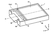
図1は、本発明の実施例に係る電気光学装置1の構成例を示す図であり、図1−1は実施例に係る電気光学装置1の斜視図、図1−2は図1−1のA−A断面図を示している。
[Structure of electro-optical device]
FIG. 1 is a diagram illustrating a configuration example of an electro-optical device 1 according to an embodiment of the present invention, FIG. 1-1 is a perspective view of the electro-optical device 1 according to the embodiment, and FIG. The AA sectional drawing of is shown.
図1に示すように、電気光学装置1は、画像を表示するための液晶表示パネル10と、液晶表示パネル10の両面に貼付けられた第1偏光板20および第2偏光板30と、液晶表示パネル10に照明光を照射するためのバックライト部40と、バックライト部40の光を表示面側に反射する反射板50と、光源であるLED60と、液晶表示パネル10の第2基板にCOG実装されたドライバIC(半導体素子)70と、液晶表示パネル10の第2基板から反射板50の裏面側に引き回され、バックライト部40の側方にLED60が配置されるように実装するFPC(Flexible Printed Circuits:配線基板)80とを、例えばプラスチックからなり、枠形状を呈する反射ケース90内に収容して構成される。
As shown in FIG. 1, the electro-optical device 1 includes a liquid
液晶表示パネル10は、対向して配置された二枚の第1基板10aおよび第2基板10bの間に液晶が封入されて構成されている。第1基板10aおよび第2基板10bはガラスで構成される。第1基板10aには、不図示のカラーフィルタ、ITO膜で形成された第1の駆動電極、および配向膜等が形成されている。第1基板10aの光出射側の面には、外周に突起部10a1が形成されている。第2基板10bには、不図示のTFDやTFT等のスイッチング素子、ITO膜で形成された第2の駆動電極、および配向膜等が形成されている。第2基板10bの光入射側の面には、外周に突起部10b1が形成されている。また、第2基板10bは、第1基板10aよりもY軸方向に平面的に突き出た突き出し部10b2を有している。
The liquid
この突き出し部10b2の表面には、液晶表示パネル10を駆動するためのドライバIC70がCOG実装されており、また、突き出し部10b2の表面端部には、ドライバIC70およびLED60に駆動信号を供給するためのFPC80がACF等で実装されている。なお、ドライバIC70は、COG実装する構成に限られるものではなく、FPC80に実装するCOF構造(Chip On Film)を採用することにしても良い。このFPC80は内側に折り曲げられ、反射板50に両面テープ(不図示)で固定される。
A driver IC 70 for driving the liquid
この液晶表示パネル10では、対向して配置された二枚の第1基板10aおよび第2基板10bに形成された第1の駆動電極および第2の駆動電極間に電荷を与えて電界を形成し、カラーフィルタに対応した位置の液晶の配向を変化させて画素を点灯/消灯させる。
In the liquid
第1基板10aおよび第2基板10bの背面側(光射出側および光入射側)の面には、使用する液晶の種類、すなわち、TN(ツイステッドネマティック)モード、STN(スーパーTN)モード、D−STN(ダブル−STN)モード等々の動作モードや、ノーマリホワイトモード/ノーマリブラックモードの別に応じて、第1偏光板20および第2偏光板30が所定の向きに貼付配置される。
On the back side (light emission side and light incident side) surfaces of the
第1偏光板20および第2偏光板30は、ポリビニルアルコール(PVA)フィルムを一方向に延伸し、ヨウ素または2色性色素を含む溶液に浸すことにより、ヨウ素または2色性色素を吸着させ、偏向機能を与え、更に保護膜としてセルロース系のフィルムを被覆して作製する。また、第1偏光板20および第2偏光板30の偏光方向は、PVAフィルムの延伸方向で決定される。
The first polarizing
第2偏光板30の下側には、バックライト部40が設けられている。バックライト部40は、その側方に配置されたLED60から発せられた照明光を導光する導光板と、導光板から出射される照明光を拡散する拡散シートと、および拡散シートで拡散された照明光を偏光するプリズムシート等から構成することができる。バックライト部40は、例えば、遮光両面テープで反射ケース90に固定することができる。バックライト部40の下面側には、バックライト部40から射出される照明光を表示面側に反射する反射板50が配置されている。この反射板50は、反射ケース90に両面テープで固定することができる。
A
[第1偏光板20および第2偏光板30]
図2は、第1偏光板20および第2偏光板30の構成の一例を示す断面図である。第1偏光板20および第2偏光板30は、図2に示すように、PVAフィルム等からなる偏光機能を有する偏光層101と、偏光層101の下面に形成された透明接着剤からなる接着層102と、接着層102の下面に形成された剥離可能なシート状の第1保護膜103と、偏光層101の上面に形成された剥離可能なシート状の第2保護膜104とで構成されている。
[First
FIG. 2 is a cross-sectional view illustrating an example of the configuration of the first
[液晶表示パネル10]
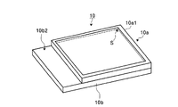
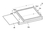
図3は、液晶表示パネル10の斜視図である。図3に示すように、液晶表示パネル10の第1基板10aには、外周に沿ってその非表示エリアに枠状の突起部10a1が形成されている。また、第2基板10bにも同様に、外周に沿ってその非表示エリアに枠状の突起部10b1(図1参照)が形成されている。突起部10a1の少なくとも1つの角(例えば、S部)を基準にして、偏光板、ドライバIC、およびFPC等の電気光学装置の構成物品の組み付けが行われる。
[Liquid Crystal Display Panel 10]
FIG. 3 is a perspective view of the liquid
[液晶表示パネル10の突起部の形成方法]
図4は、液晶表示パネル10の突起部の形成方法を説明するための説明図である。図4において、多面取り可能な2枚の大判基板を使用して、液晶表示パネルの製造工程を実行して、複数の液晶表示パネル(同図に示す例では、5×4)10を含む大判パネル構造体200を形成する(大判パネル構造体製造工程)。
[Method for Forming Projection of Liquid Crystal Display Panel 10]
FIG. 4 is an explanatory diagram for explaining a method of forming the protrusions of the liquid
つぎに、フォトリソグラフィ法を使用して、大判パネル構造体200の各液晶表示パネル10の外周に突起部10a1,10b1を形成する(突起部形成工程)。具体的には、大判パネル構造体にフォトレジストを塗布した後、多面取りフォトマスクを使用して、露光装置で露光を行う。この後、現像・エッチング・剥離の工程を施すことで、大判パネル構造体の各液晶表示パネル10の外周に突起部10a1を形成することができる。同様な方法で突起部10b1を形成する。
Next, using the photolithography method, the protrusions 10a1 and 10b1 are formed on the outer periphery of each liquid
大判パネル構造体200を切断し単一の液晶表示パネル10毎に分離する(切断工程)。これにより図6に示すような単一の液晶表示パネル10が切り出され、5×4枚の液晶表示パネル10が製造される。
The
[偏光板20および偏光板30の貼付方法]
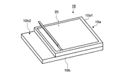
図5は、液晶表示パネル10に偏光板20を貼り付ける方法を説明するための図である。図5において、液晶表示パネル10の第1基板10aの突起部10a1の少なくとも1つの角(例えば、図3において、S部)を基準にして、その内側に第1偏光板20を貼り付ける。このように、液晶表示パネル10に形成された突起部10a1を基準にして、第1偏光板20を貼り付けているので、液晶表示パネルの辺や角などといった外形形状を基準にして偏光板を位置合わせする方法と比較して、第1偏光板20の貼付位置や向きが液晶表示パネルの外形形状の精度に左右されることがない。従って、液晶表示パネル10に対する第1偏光板20の位置や向きを高い精度で合わせることができる。また、突起部10a1の厚さが、第1偏光板20の厚さと略同一に形成されているので、突起部10a1が目立つことはなく、突起部10a1が液晶表示パネル10の美観を損なうことはない。
[Pasting method of polarizing
FIG. 5 is a diagram for explaining a method of attaching the
第2基板10bにも同様に、外周に沿ってその非表示エリアに枠状の突起部10b1が形成されており、この突起部10b1を基準に第2偏光板30を貼り付ける。
Similarly, a frame-like protrusion 10b1 is formed in the non-display area along the outer periphery of the
[ドライバIC70の実装方法]
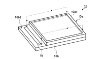
図6は、液晶表示パネル10にドライバIC70を実装する方法を説明するための図である。図6において、液晶表示パネル10の第1基板10aの突起部10a1の少なくとも1つの角(例えば、図3において、S部)を基準にして、第2基板10bの突き出し部10b2の表面に、ACF等でドライバIC70を実装する。このように、液晶表示パネル10の第1基板10aの突起部10a1を基準にしてFPC80を実装しているので、アライメントマークを合わせて位置決めする必要がなくなり、カメラユニット等の高価な位置決め装置が不要となり、簡単かつ低コストにドライバIC70を実装することができる。
[Method of mounting driver IC 70]
FIG. 6 is a diagram for explaining a method of mounting the
[FPC80の実装方法]
図7は、液晶表示パネル10にFPC80を実装する方法を説明するための図である。図7において、液晶表示パネル10の第1基板10aの突起部10a1の少なくとも1つの角(例えば、図3において、S部)を基準にして、第2基板10bの突き出し部10b2の表面端部に、ACF等でFPC80を実装する。このように、液晶表示パネル10の第1基板10aの突起部10a1を基準にしてFPC80を実装しているので、アライメントマークを合わせて位置決めする必要がなくなり、カメラユニット等の高価な位置決め装置が不要となり、簡単かつ低コストにFPC80を実装することができる。
[FPC80 mounting method]
FIG. 7 is a diagram for explaining a method of mounting the
(変形例)
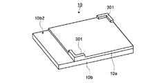
図8は、変形例に係る液晶表示パネル10の斜視図を示している。上記実施例では、液晶表示パネル10の外周に沿って突起部10a1を設ける構成としたが、図8に示すように、液晶表示パネル10の非表示エリアの一部に突起部301を形成する構成としても良い。偏光板、ドライバIC、およびFPC等の電気光学装置の構成物品の組み付けは、この突起部301を基準に行う。
(Modification)
FIG. 8 is a perspective view of a liquid
(電子機器への適用例)
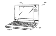
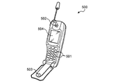
次に、本発明に係る電気光学装置を適用可能な電子機器の具体例について図9を参照して説明する。図9−1は、本発明に係る電気光学装置を可搬型のパーソナルコンピュータ(いわゆるノート型パソコン)400の表示部に適用した例を示す斜視図である。同図に示すように、パーソナルコンピュータ400は、キーボード401を備えた本体部402と、本発明に係る電気光学装置を適用した表示部403とを備えている。図9−2は、本発明に係る電気光学装置を携帯電話機500の表示部に適用した例を示す斜視図である。同図に示すように、携帯電話機500は、複数の操作ボタン501のほか、受話口502、送話口503とともに、本発明に係る電気光学装置を適用した表示部504を備えている。
(Application example to electronic equipment)
Next, specific examples of electronic devices to which the electro-optical device according to the invention can be applied will be described with reference to FIG. FIG. 9A is a perspective view illustrating an example in which the electro-optical device according to the invention is applied to a display unit of a portable personal computer 400 (so-called notebook computer). As shown in the figure, the
本発明にかかる電気光学装置は、透過型、反射型、および半透過型の電気光学装置に利用することができる。また、本発明にかかる電気光学装置は、パッシブマトリクス型の電気光学装置やアクティブマトリクス型の電気光学装置(例えば、TFT(薄膜トランジスタ)やTFD(薄膜ダイオード)をスイッチング素子として備えた電気光学パネル)に利用することができる。さらに、本発明にかかる電気光学装置は、液晶表示装置に限らず、有機エレクトロルミネッセンス装置、無機エレクトロルミネッセンス装置、プラズマディスプレイ装置、電気泳動表示装置、電子放出表示装置(Field Emission DisplayおよびSurface-Conduction Electoron-Emitter Display等)、LED(ライトエミッティングダイオード)表示装置等のように、複数の画素毎に表示状態を制御可能な各種の電気光学装置に利用することができる。 The electro-optical device according to the present invention can be used for transmissive, reflective, and transflective electro-optical devices. The electro-optical device according to the present invention is applied to a passive matrix type electro-optical device or an active matrix type electro-optical device (for example, an electro-optical panel including a TFT (thin film transistor) or a TFD (thin film diode) as a switching element). Can be used. Furthermore, the electro-optical device according to the present invention is not limited to a liquid crystal display device, but is an organic electroluminescence device, an inorganic electroluminescence device, a plasma display device, an electrophoretic display device, an electron emission display device (Field Emission Display and Surface-Conduction Electoron). -Emitter Display etc.), LED (Light Emitting Diode) display devices, etc., and can be used for various electro-optical devices that can control the display state for each of a plurality of pixels.
本発明にかかる電気光学装置を搭載した電子機器は、携帯電話機、PDA(Personal Digital Assistants)と呼ばれる携帯型情報機器、携帯型パーソナルコンピュータ、パーソナルコンピュータ、ワークステーション、デジタルスチルカメラ、車載用モニタ、デジタルビデオカメラ、液晶テレビ、ビューファインダ型、モニタ直視型のビデオテープレコーダ、カーナビゲーション装置、ページャ、電子手帳、電卓、ワードプロセッサ、ワークステーション、テレビ電話機、およびPOS端末機などの電子機器に広く利用することができる。 An electronic device equipped with the electro-optical device according to the present invention includes a mobile phone, a portable information device called PDA (Personal Digital Assistants), a portable personal computer, a personal computer, a workstation, a digital still camera, an in-vehicle monitor, a digital Widely used in electronic devices such as video cameras, LCD TVs, viewfinder type, monitor direct-view type video tape recorders, car navigation devices, pagers, electronic notebooks, calculators, word processors, workstations, video phones, and POS terminals. Can do.
1 電気光学装置、10 液晶表示パネル、10a 第1基板、10b 第2基板、20 第1偏光板、30 第2偏光板、40 バックライト部、50 反射板、60 LED、70 ドライバIC、80 FPC、90 反射ケース、100 大判偏光板構造体、101 偏光層、102 接着層、103 第1保護膜、104 第2保護膜、200 大判パネル構造体、201 突起部、400 パーソナルコンピュータ、401 キーボード、402 本体部、403 表示部、500 携帯電話機、501 操作ボタン、502 受話口、503 送話口、504 表示部 DESCRIPTION OF SYMBOLS 1 Electro-optical device, 10 Liquid crystal display panel, 10a 1st board | substrate, 10b 2nd board | substrate, 20 1st polarizing plate, 30 2nd polarizing plate, 40 Backlight part, 50 Reflector, 60 LED, 70 Driver IC, 80 FPC , 90 Reflective case, 100 Large polarizing plate structure, 101 Polarizing layer, 102 Adhesive layer, 103 First protective film, 104 Second protective film, 200 Large panel structure, 201 Protrusion, 400 Personal computer, 401 Keyboard, 402 Main unit, 403 display unit, 500 mobile phone, 501 operation button, 502 earpiece, 503 mouthpiece, 504 display unit
Claims (9)
前記電気光学パネルの前記突起部を基準にして、前記電気光学パネルに電気光学装置の構成物品を組み付ける組み付け工程と、
を含むことを特徴とする電気光学装置の製造方法。 A protrusion forming step of forming a protrusion on a part of the non-display area of at least one surface of the electro-optic panel;
An assembling step of assembling a component of an electro-optical device to the electro-optical panel based on the protrusion of the electro-optical panel;
A method for manufacturing an electro-optical device.
Priority Applications (1)
| Application Number | Priority Date | Filing Date | Title |
|---|---|---|---|
| JP2004104310A JP2005292285A (en) | 2004-03-31 | 2004-03-31 | Electro-optical device manufacturing method and electronic apparatus |
Applications Claiming Priority (1)
| Application Number | Priority Date | Filing Date | Title |
|---|---|---|---|
| JP2004104310A JP2005292285A (en) | 2004-03-31 | 2004-03-31 | Electro-optical device manufacturing method and electronic apparatus |
Publications (1)
| Publication Number | Publication Date |
|---|---|
| JP2005292285A true JP2005292285A (en) | 2005-10-20 |
Family
ID=35325309
Family Applications (1)
| Application Number | Title | Priority Date | Filing Date |
|---|---|---|---|
| JP2004104310A Withdrawn JP2005292285A (en) | 2004-03-31 | 2004-03-31 | Electro-optical device manufacturing method and electronic apparatus |
Country Status (1)
| Country | Link |
|---|---|
| JP (1) | JP2005292285A (en) |
Cited By (1)
| Publication number | Priority date | Publication date | Assignee | Title |
|---|---|---|---|---|
| KR20160078665A (en) * | 2014-12-24 | 2016-07-05 | 삼성디스플레이 주식회사 | Window for display device and display device comprising the same |
-
2004
- 2004-03-31 JP JP2004104310A patent/JP2005292285A/en not_active Withdrawn
Cited By (2)
| Publication number | Priority date | Publication date | Assignee | Title |
|---|---|---|---|---|
| KR20160078665A (en) * | 2014-12-24 | 2016-07-05 | 삼성디스플레이 주식회사 | Window for display device and display device comprising the same |
| KR102404930B1 (en) * | 2014-12-24 | 2022-06-08 | 삼성디스플레이 주식회사 | Window for display device and display device comprising the same |
Similar Documents
| Publication | Publication Date | Title |
|---|---|---|
| CN103119505B (en) | LCD Modules and Electronics | |
| US7580103B2 (en) | Electro-optical device, method of mounting wiring substrate, and electronic apparatus | |
| US20050286008A1 (en) | Electro-optical device and electronic apparatus | |
| JP4333727B2 (en) | ELECTRO-OPTICAL DEVICE, LIGHTING DEVICE, AND ELECTRONIC DEVICE | |
| CN111708206B (en) | Touch display module, manufacturing method thereof and display device | |
| JP2005338155A (en) | Electro-optical device and electronic apparatus | |
| KR20040098590A (en) | Electro-optical device, electronic apparatus, and method of manufacturing the electro-optical device | |
| KR20040098606A (en) | Electro-optical device, electronic apparatus, and method of manufacturing the electro-optical device | |
| JP2009217116A (en) | Liquid crystal display device | |
| JP2007114444A (en) | Liquid crystal display | |
| US20180107062A1 (en) | Backlight module and assembly method thereof | |
| JP2005084510A (en) | Electro-optical device and electronic apparatus including electro-optical device | |
| JP2008176237A (en) | Liquid crystal display | |
| JP2005266284A (en) | ELECTRO-OPTICAL DEVICE MANUFACTURING METHOD, ELECTRONIC DEVICE HAVING ELECTRO-OPTICAL DEVICE PRODUCED BY THE MANUFACTURING METHOD, AND POLARIZER | |
| CN1717166B (en) | Display device and apparatus | |
| JP2000267077A (en) | Liquid crystal display and electronic equipment | |
| JP2005099619A (en) | Electro-optical device and electronic apparatus including the electro-optical device | |
| JP4122920B2 (en) | Electro-optical device manufacturing method, flexible substrate, electro-optical device, and electronic apparatus | |
| JP2004336293A (en) | Electro-optical device with sounding body, method of manufacturing electro-optical device with sounding body, and electronic apparatus | |
| JP2005292284A (en) | Mounting structure, electro-optical device, and electronic apparatus | |
| JP4760571B2 (en) | Liquid crystal device, lighting device and electronic apparatus | |
| JP2006284978A (en) | Electrooptical device and electronic apparatus | |
| JP4461753B2 (en) | Liquid crystal device and electronic device | |
| JP2005277160A (en) | Mounting structure manufacturing method, mounting structure, electro-optical device, and electronic apparatus | |
| JP2005283829A (en) | Electro-optical device and electronic apparatus |
Legal Events
| Date | Code | Title | Description |
|---|---|---|---|
| A300 | Withdrawal of application because of no request for examination |
Free format text: JAPANESE INTERMEDIATE CODE: A300 Effective date: 20070605 |