JP2005292258A - Display device - Google Patents
Display device Download PDFInfo
- Publication number
- JP2005292258A JP2005292258A JP2004103916A JP2004103916A JP2005292258A JP 2005292258 A JP2005292258 A JP 2005292258A JP 2004103916 A JP2004103916 A JP 2004103916A JP 2004103916 A JP2004103916 A JP 2004103916A JP 2005292258 A JP2005292258 A JP 2005292258A
- Authority
- JP
- Japan
- Prior art keywords
- substrate
- electrolyte solution
- display device
- electrode
- display
- Prior art date
- Legal status (The legal status is an assumption and is not a legal conclusion. Google has not performed a legal analysis and makes no representation as to the accuracy of the status listed.)
- Granted
Links
Images

Landscapes
- Electrochromic Elements, Electrophoresis, Or Variable Reflection Or Absorption Elements (AREA)
- Devices For Indicating Variable Information By Combining Individual Elements (AREA)
Abstract
【課題】 高品位の表示を長期間にわたって安定して得ることができる、ECL発光型、EC反射型、及びECL・EC型の表示装置を提供すること。
【解決手段】 第一基板と、この第一基板に離間対向して設けられた第二基板と、前記第一基板若しくは前記第二基板に設けられた第一電極と、前記第一基板若しくは前記第二基板に設けられた第二電極と、前記第一基板と前記第二基板との間に配置された電解質溶液層とを具備してなり、前記電解質溶液層を介して前記第一電極と前記第二電極との間に電圧を印加することによって表示を行うように構成された表示装置であって、前記電解質溶液層中の電解質溶液を交換可能に設けられた電解質溶液貯留部を有することを特徴とする、表示装置。
【選択図】 図1PROBLEM TO BE SOLVED: To provide an ECL light emission type, an EC reflection type, and an ECL / EC type display device capable of stably obtaining a high-quality display over a long period of time.
A first substrate, a second substrate provided to be spaced apart from the first substrate, a first electrode provided on the first substrate or the second substrate, the first substrate, or the first substrate A second electrode provided on the second substrate; and an electrolyte solution layer disposed between the first substrate and the second substrate; and the first electrode via the electrolyte solution layer A display device configured to perform display by applying a voltage between the second electrode and an electrolyte solution storage unit provided to replace the electrolyte solution in the electrolyte solution layer. A display device.
[Selection] Figure 1
Description
本発明は、エレクトロケミルミネッセンス(ECL)を示す表示装置、エレクトロクロミズム(EC)を示す表示装置、およびエレクトロケミルミネッセンス(ECL)とエレクトロクロミズム(EC)両方を示す表示装置に関するものである。 The present invention relates to a display device that exhibits electrochemiluminescence (ECL), a display device that exhibits electrochromism (EC), and a display device that exhibits both electrochemiluminescence (ECL) and electrochromism (EC).
明るい反射表示を可能とするディスプレイとして、エレクトロクロミック、エレクトロクロミズム(以下、「EC」と言うことがある)ディスプレイがある。この表示装置としては、電気化学的な酸化もしくは還元反応により変色、もしくは析出、もしくは溶解する着色用物質(EC材料)と、電解質とが、第一電極と第二電極との間に配置されている構造からなるもの(例えば、特許文献1参照)が知られている。しかしながら、電解質の劣化などにより寿命が短く実用化が難しかった。 There are electrochromic and electrochromic (hereinafter, sometimes referred to as “EC”) displays as displays that enable bright reflective display. In this display device, a coloring substance (EC material) that changes color, precipitates, or dissolves by an electrochemical oxidation or reduction reaction, and an electrolyte are disposed between a first electrode and a second electrode. There is a known structure (for example, see Patent Document 1). However, due to the deterioration of the electrolyte and the like, the lifetime was short and it was difficult to put it to practical use.
また、液晶ディスプレイ(LCD)と同様な液体を内包したセル構造で発光表示が可能なディスプレイとして、エレクトロケミルミネッセンス(以下、「ECL」と言うことがある)ディスプレイがある。この表示装置としては、電気化学的な酸化もしくは還元反応により発生したイオンラジカル種が反応して発光する発光用物質(ECL材料)と、電解質とが、第一電極と第二電極との間に配置されている構造からなるもの(例えば、特許文献2参照)が知られている。しかしながら、ECディスプレイと同様に、電解質の劣化などにより寿命が短く実用化が難しかった。
ECLやECを利用する表示装置には、上記の通りにECL材料やEC材料および電解質溶液の劣化の問題があって、高品位の表示を長期間にわたって安定して得ることが困難であった。 As described above, the display device using ECL and EC has a problem of deterioration of the ECL material, the EC material, and the electrolyte solution, and it has been difficult to stably obtain a high-quality display over a long period of time.
特に、ECLを利用した表示装置において、駆動電圧の低減等のために第一電極と第二電極との間隔を狭めたものの場合には、電解質およびECL材料の量が少ないことから電解質劣化による影響が早期に観察されるようになる。 In particular, in the case of a display device using ECL, in which the distance between the first electrode and the second electrode is narrowed to reduce the driving voltage, the amount of the electrolyte and the ECL material is small, and therefore the influence of the electrolyte deterioration. Will be observed early.
この問題に鑑み、本発明は、長寿命を実現するECディスプレイ、ECLディスプレイ、およびEC・ECLディスプレイを提供することを目的とする。 In view of this problem, an object of the present invention is to provide an EC display, an ECL display, and an EC / ECL display that achieve a long life.
従って、本発明による表示装置は、第一基板と、この第一基板に離間対向して設けられた第二基板と、前記第一基板若しくは前記第二基板に設けられた第一電極と、前記第一基板若しくは前記第二基板に設けられた第二電極と、前記第一基板と前記第二基板との間に配置された電解質溶液層とを具備してなり、前記電解質溶液層を介して前記第一電極と前記第二電極との間に電圧を印加することによって表示を行うように構成された表示装置であって、前記電解質溶液層中の電解質溶液を交換可能に設けられた電解質溶液貯留部を有すること、を特徴とするものである。 Accordingly, the display device according to the present invention includes a first substrate, a second substrate provided to be spaced apart from the first substrate, the first electrode provided on the first substrate or the second substrate, A second electrode provided on the first substrate or the second substrate, and an electrolyte solution layer disposed between the first substrate and the second substrate, with the electrolyte solution layer interposed therebetween. A display device configured to perform display by applying a voltage between the first electrode and the second electrode, wherein the electrolyte solution in the electrolyte solution layer is provided to be replaceable It has the storage part.
このような本発明による表示装置は、好ましくは、前記電解質溶液が、電気化学的な酸化もしくは還元反応により発光する発光材料を含有するものとすることができる。 In such a display device according to the present invention, preferably, the electrolyte solution may contain a light emitting material that emits light by an electrochemical oxidation or reduction reaction.
このような本発明による表示装置は、好ましくは、同一の密閉セル内に、前記第一基板、前記第二基板、前記電解質溶液層および前記電解質溶液貯留部を有するものとすることができる。 Such a display device according to the present invention may preferably include the first substrate, the second substrate, the electrolyte solution layer, and the electrolyte solution reservoir in the same sealed cell.
このような本発明による表示装置は、好ましくは、前記第一基板が前記密閉セルの内壁面に固定され、一方前記第二基板が前記密閉セル内部に架設されて、前記第二基板の前記第一基板側には前記電解質溶液層が形成されるとともに、前記第二基板の反対面側には前記電解質溶液貯留部が形成されているものとすることができる。 In such a display device according to the present invention, preferably, the first substrate is fixed to the inner wall surface of the sealed cell, while the second substrate is installed inside the sealed cell, The electrolyte solution layer may be formed on one substrate side, and the electrolyte solution storage portion may be formed on the opposite surface side of the second substrate.
このような本発明による表示装置は、好ましくは、前記第二基板が多孔質基板であるものとすることができる。 In such a display device according to the present invention, preferably, the second substrate may be a porous substrate.
このような本発明による表示装置は、好ましくは、前記第一電極が前記第一基板に設けられ、前記第二電極が前記第二基板に前記第一電極と対向するよう設けられ、さらに前記第一基板には前記第二電極と対向するよう第三電極が設けられ、前記第二電極の前記第一電極側の表面に電気化学的な酸化もしくは還元反応によって変色する着色材料を含む固体層が形成されているものとすることができる。 In such a display device according to the present invention, preferably, the first electrode is provided on the first substrate, the second electrode is provided on the second substrate so as to face the first electrode, and the first electrode is further provided. A third electrode is provided on one substrate so as to face the second electrode, and a surface of the second electrode on the first electrode side has a solid layer containing a coloring material that changes color by an electrochemical oxidation or reduction reaction. It may be formed.
このような本発明による表示装置は、好ましくは、前記密閉セルの少なくとも一部分が高分子フィルムによって形成されているものとすることができる。 In such a display device according to the present invention, it is preferable that at least a part of the sealed cell is formed of a polymer film.
このような本発明による表示装置は、好ましくは、前記電解質溶液貯留部内に存在する電解質溶液の量が、前記電解質溶液層を形成している電解質溶液の量より多いものとすることができる。 In such a display device according to the present invention, it is preferable that the amount of the electrolyte solution present in the electrolyte solution reservoir is larger than the amount of the electrolyte solution forming the electrolyte solution layer.
このような本発明による表示装置は、好ましくは、前記電解質溶液層および前記電解質溶液貯留部に存在する電解質溶液を前記密閉セルの外部と交換可能に構成されたものとすることができる。 Such a display device according to the present invention may be preferably configured so that the electrolyte solution existing in the electrolyte solution layer and the electrolyte solution reservoir can be exchanged with the outside of the sealed cell.
本発明による表示装置は、電解質溶液層を介して対向する二つの基板との間に電圧を印加することによって表示を行うように構成された表示装置であって、前記電解質溶液層中の電解質溶液を交換可能に設けられた電解質溶液貯留部を有することから、発光表示および(または)反射表示が行なわれる電解質溶液層中のECL材料やEC材料および電解質溶液の劣化による問題が解消される。 A display device according to the present invention is a display device configured to perform display by applying a voltage between two opposing substrates via an electrolyte solution layer, the electrolyte solution in the electrolyte solution layer Therefore, the problem caused by the deterioration of the ECL material, the EC material, and the electrolyte solution in the electrolyte solution layer in which the light emission display and / or the reflection display is performed is solved.
従って、このような本発明によれば、高品位の表示を長期間にわたって安定して得ることができる表示装置が提供される。 Therefore, according to the present invention, a display device capable of stably obtaining a high-quality display over a long period of time is provided.
<表示装置>
以下に、本発明の実施形態に係る表示装置について詳細に説明する。
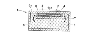
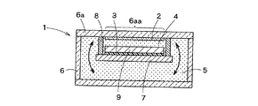
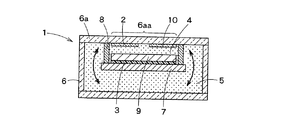
図1〜図3は、本発明による表示装置の好ましい具体例ついてその概要を示す断面図である。図1はECLを利用して表示を行う装置(以下、「発光表示装置」と言うことがある)に関連するものであり、図2はECの反射表示を行う装置(以下、「反射表示装置」と言うことがある)に関連するものであり、図3はECLおよびECの両者を利用して表示を行う装置(以下、「発光・反射表示装置」と言うことがある)に関連するものである。
<Display device>
Below, the display apparatus which concerns on embodiment of this invention is demonstrated in detail.
1 to 3 are sectional views showing an outline of a preferred specific example of a display device according to the present invention. FIG. 1 relates to a device that performs display using ECL (hereinafter sometimes referred to as “light-emitting display device”), and FIG. 2 illustrates a device that performs EC reflective display (hereinafter referred to as “reflective display device”). FIG. 3 relates to a device that performs display using both ECL and EC (hereinafter sometimes referred to as “light emitting / reflective display device”). It is.
基本構造
図1〜図3に示される本発明による表示装置(1)は、第一基板(2)と、この第一基板(2)に離間対向して設けられた第二基板(3)と、前記第一基板(2)若しくは前記第二基板(3)に設けられた第一電極と、前記第一基板(2)若しくは前記第二基板(3)に設けられた第二電極と、前記第一基板(2)と前記第二基板(3)との間に配置された電解質溶液層(4)とを具備してなり、前記電解質溶液層(4)を介して前記第一電極と前記第二電極との間に電圧を印加することによって表示を行うように構成された表示装置であって、前記電解質溶液層中の電解質溶液を交換可能に設けられた電解質溶液貯留部(5)を有するものである。
Basic structure
The display device (1) according to the present invention shown in FIGS. 1 to 3 includes a first substrate (2), a second substrate (3) provided opposite to the first substrate (2), A first electrode provided on the first substrate (2) or the second substrate (3); a second electrode provided on the first substrate (2) or the second substrate (3); An electrolyte solution layer (4) disposed between the substrate (2) and the second substrate (3), wherein the first electrode and the second electrode are interposed via the electrolyte solution layer (4). A display device configured to perform display by applying a voltage between the electrodes and having an electrolyte solution storage section (5) provided so that the electrolyte solution in the electrolyte solution layer can be replaced It is.
このような本発明による表示装置(1)において、電解質溶液層(4)は、電解質溶液または電気化学的な酸化もしくは還元反応により発光する発光材料を含有する電解質溶液によって形成されており、そして同様の電解質溶液が電解質溶液貯留部(5)に充填されて、前記電解質溶液層(4)中の電解質溶液と電解質溶液貯留部(5)中の電解質溶液とが交換可能になっている。なお、本明細書において、「電解質溶液層」とは、第一基板(2)と第二基板(3)との間の電解質溶液からなる層のことを言い、「電解質溶液貯留部」とは、前記電解質溶液層中の電解質溶液と交換可能な電解質溶液層が充填されている部分をいう。「電解質溶液貯留部」の容量は、大きければ大きい方が好ましい。用途で決まるディスプレイの厚さの許容範囲に収まれば良い。例えば、1倍〜100倍程度とすることができる。 In such a display device (1) according to the present invention, the electrolyte solution layer (4) is formed of an electrolyte solution or an electrolyte solution containing a luminescent material that emits light by an electrochemical oxidation or reduction reaction, and the like. The electrolyte solution storage part (5) is filled with the electrolyte solution, and the electrolyte solution in the electrolyte solution layer (4) and the electrolyte solution in the electrolyte solution storage part (5) can be exchanged. In the present specification, the “electrolyte solution layer” means a layer made of an electrolyte solution between the first substrate (2) and the second substrate (3), and the “electrolyte solution reservoir” The part in which the electrolyte solution layer exchangeable with the electrolyte solution in the electrolyte solution layer is filled. The capacity of the “electrolyte solution reservoir” is preferably as large as possible. It suffices to be within the allowable range of the display thickness determined by the application. For example, it can be about 1 to 100 times.
そして、上記の第一基板(2)、第二基板(3)、電解質溶液層(4)および電解質溶液貯留部(5)は同一の密閉セル内(6)に存在している。そして、この密閉セル(6)内部には、電解質溶液層(4)を形成している電解質溶液と、それより十分に多い量の電解質溶液が電解質溶液貯留部(5)に存在している。電解質溶液層(4)の厚さは、例えば、1μm〜20μm程度とすることができる。 And said 1st board | substrate (2), 2nd board | substrate (3), electrolyte solution layer (4), and electrolyte solution storage part (5) exist in the same sealed cell (6). In the closed cell (6), the electrolyte solution forming the electrolyte solution layer (4) and a sufficiently larger amount of the electrolyte solution are present in the electrolyte solution reservoir (5). The thickness of the electrolyte solution layer (4) can be, for example, about 1 μm to 20 μm.
第一基板(2)は、前記密閉セル(6)の内壁面に固定されている。一方、第二基板(3)は、前記密閉セル(6)内部に架設されて、この第二基板(3)の第一基板(2)側には電解質溶液層(4)が形成されるとともに、第二基板(3)の反対面側には電解質溶液貯留部(5)が形成されている。なお、支持基板(7)は、第二基板(3)自体が十分な強度・剛性を有している物である場合には必須ではないが、本発明では、第二基板(3)を支持基板(7)上に形成し前記密閉セル(6)内部に架設することが好ましい。この場合、図1〜図3に示されるように、第一基板(2)が形成された基板(6a)と、第二基板(3)が形成された支持基板(7)とを、適当なスペーサ(8)等を用いて固定することによって、密閉セル(6)内部に第二基板(3)を架設することが好ましい。支持基板(7)が、電解質溶液を透過可能な多孔質基板である場合には、電解質溶液層(4)中の電解質溶液と電解質溶液貯留部(5)中の電解質溶液との交換をより効率的に行うことができることから、好ましい。 The first substrate (2) is fixed to the inner wall surface of the closed cell (6). On the other hand, the second substrate (3) is installed inside the sealed cell (6), and an electrolyte solution layer (4) is formed on the first substrate (2) side of the second substrate (3). An electrolyte solution reservoir (5) is formed on the opposite side of the second substrate (3). The support substrate (7) is not essential when the second substrate (3) itself has sufficient strength and rigidity, but in the present invention, the second substrate (3) is supported. It is preferably formed on the substrate (7) and installed inside the closed cell (6). In this case, as shown in FIGS. 1 to 3, the substrate (6a) on which the first substrate (2) is formed and the support substrate (7) on which the second substrate (3) is formed are appropriately combined. The second substrate (3) is preferably installed inside the sealed cell (6) by fixing it with a spacer (8) or the like. When the support substrate (7) is a porous substrate that can permeate the electrolyte solution, it is more efficient to exchange the electrolyte solution in the electrolyte solution layer (4) and the electrolyte solution in the electrolyte solution reservoir (5). This is preferable because it can be carried out automatically.
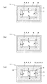
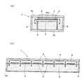
図4(a)は図1の表示装置の上面図であり、図4(b)は図2の表示装置の上面図であり、図4(c)は図3の表示装置の上面図である。 4A is a top view of the display device of FIG. 1, FIG. 4B is a top view of the display device of FIG. 2, and FIG. 4C is a top view of the display device of FIG. .
なお、本発明において、第二基板(3)の架設方法は、本発明の目的および効果が達成されるならば、図1〜図3に具体的に示される以外の任意の方法を採用することができる。例えば図5(a)に示されるように、支持基板(7)を密閉セル(6)の底面部(6c)にスペーサ(8)等を用いて固定することもできるし、図5(b)に示されるように、支持基板(7)を密閉セル(6)の側壁部(6b)に固定することもできる。図5(a)の表示装置では電解質溶液層(4)の面積(即ち、表示面積)を拡大することができ、図5(b)の表示装置では、同一密閉セル中(6)に複数の電解質溶液層(4)(即ち、複数の表示部)を形成する場合に有利である。 In the present invention, any method other than that specifically shown in FIGS. 1 to 3 may be adopted as a method of laying the second substrate (3) as long as the objects and effects of the present invention are achieved. Can do. For example, as shown in FIG. 5 (a), the support substrate (7) can be fixed to the bottom surface portion (6c) of the sealed cell (6) using a spacer (8) or the like, or FIG. As shown in FIG. 4, the support substrate (7) can be fixed to the side wall (6b) of the closed cell (6). In the display device of FIG. 5 (a), the area of the electrolyte solution layer (4) (that is, the display area) can be enlarged, and in the display device of FIG. This is advantageous when the electrolyte solution layer (4) (that is, a plurality of display portions) is formed.
図1〜図3に示される表示装置(1)において、第一基板(2)が設けられている密閉セル(6)の基板(6a)は、通常、表示装置の観察面(この観察面の少なくとも一部分の領域は表示部(6aa)となる)となる部分であるから、当該部分は光透過性材料で形成するのが普通である。そのような光透過性材料としては、好ましくは可視光領域で吸収が少ない材料、例えばガラス等の無機材料、および光透過性樹脂等の有機性材料、具体的には例えば、ポリエチレンテレフタレート(PET)、ポリエチレンナフタレート(PEN)、ポリエーテルサルホン(PES)、ポリカーボネート(PC)等を挙げることができる。そして、このように基板(6a)を観察面とする場合、第一基板(2)も表示が明確に観察されるように透明な材料で形成するのが普通である。 In the display device (1) shown in FIGS. 1 to 3, the substrate (6a) of the sealed cell (6) provided with the first substrate (2) is usually an observation surface of the display device (of this observation surface). Since at least a part of the region is a portion that becomes a display portion (6aa), the portion is usually formed of a light transmissive material. As such a light transmissive material, a material having a low absorption in the visible light region, for example, an inorganic material such as glass, and an organic material such as a light transmissive resin, specifically, for example, polyethylene terephthalate (PET). , Polyethylene naphthalate (PEN), polyethersulfone (PES), polycarbonate (PC) and the like. When the substrate (6a) is used as the observation surface in this way, the first substrate (2) is usually formed of a transparent material so that the display can be clearly observed.
一方、図1〜図3に示される表示装置(1)の底面部(6c)側を表示装置の表示部とする場合には、底面部(6c)の表示部、第二基板(3)および支持基板(7)を透明な材料で形成するのが普通である。 On the other hand, in the case where the bottom surface (6c) side of the display device (1) shown in FIGS. 1 to 3 is the display device of the display device, the display portion of the bottom surface portion (6c), the second substrate (3), and The support substrate (7) is usually formed from a transparent material.
図1に示される「発光表示装置」においては必須ではないが、図2に示される「反射表示装置図」および図3に示される「発光・反射表示装置」においては、電気化学的な酸化もしくは還元反応によって変色する着色材料を含む固体層(以下、「EC層」という)(9)が形成される。このEC層(9)は、基板(6a)の一部を表示装置の表示部(6aa)とする場合には、図2および図3に示されるように、第二基板(3)の表面に形成するのが普通である。一方、密閉セル(6)の底面部(6c)を表示装置の表示部とする場合には第一基板(2)の表面に形成するのが普通である。 1 is not essential, but in the “reflection display device diagram” shown in FIG. 2 and the “light emission / reflection display device” shown in FIG. A solid layer (hereinafter referred to as “EC layer”) (9) containing a coloring material that changes color by the reduction reaction is formed. The EC layer (9) is formed on the surface of the second substrate (3) as shown in FIGS. 2 and 3 when a part of the substrate (6a) is used as the display unit (6aa) of the display device. It is common to form. On the other hand, when the bottom surface portion (6c) of the sealed cell (6) is used as the display portion of the display device, it is usually formed on the surface of the first substrate (2).
また、図3に示される「発光・反射装置」においては、第一基板(2)および第二基板(3)に離間対向して、さらに第三基板(10)が形成される。このような表示装置では、第一基板(2)、第二基板(3)および第三基板(10)の極性および印加する電圧等を制御することによって、発光表示、反射表示、および発光・反射表示を制御して行うことができるようになる。 Further, in the “light emitting / reflecting device” shown in FIG. 3, a third substrate (10) is further formed so as to be opposed to the first substrate (2) and the second substrate (3). In such a display device, by controlling the polarities of the first substrate (2), the second substrate (3), and the third substrate (10), the applied voltage, and the like, light-emitting display, reflective display, and light-emitting / reflecting are performed. The display can be controlled.
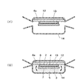
なお、高品位の表示を安定して得るためには、電解質溶液層(4)の層厚が一定でありることが有利であることから、基板(6a)および支持基板(7)は実用上の問題が発生しないように十分な強度および剛性を有するものが好ましく、かつ複数のスペーサ(8)を効果的に配置して基板(6a)と支持基板(7)との位置関係がずれないようにすることが好ましい。しかし、密閉セル(6)の基板(6a)以外の部分(図1〜図3の側壁部(6b)および(または)底面部(6c)部分)は、実用上の問題が発生しないならば、電解質溶液を密封可能な任意の材料によって形成することができる。例えば図9(ロ)に示されるように、密閉セル(6)の基板(6a)以外の部分は高分子フィルムのように柔軟な材料によって形成することができる。図9(ロ)に示されるような、高分子フィルムからなるフィルムパッケージを密封セル(6)とする表示装置は、本発明に好ましい一具体例である。
In order to stably obtain a high-quality display, it is advantageous that the thickness of the electrolyte solution layer (4) is constant, so that the substrate (6a) and the support substrate (7) are practically used. In order to prevent this problem, it is preferable to have sufficient strength and rigidity, and a plurality of spacers (8) are effectively arranged so that the positional relationship between the substrate (6a) and the support substrate (7) does not shift. It is preferable to make it. However, if the portion other than the substrate (6a) of the sealed cell (6) (the side wall portion (6b) and / or the bottom surface portion (6c) portion in FIGS. 1 to 3) does not cause a practical problem, The electrolyte solution can be formed of any material that can be sealed. For example, as shown in FIG. 9B, portions other than the
さらに、図1〜図3および図9(ロ)に示される本発明による表示装置においては、好ましくは、前記電解質溶液層(4)および前記電解質溶液貯留部(5)に存在する電解質溶液(この電解質溶液は、後述の通りに、各種のECL分子、溶媒および支持塩等を含む)を前記密閉セル(6)の外部と交換可能に構成されたものとすることができる。例えば、電解質溶液貯留部(5)中の電解質溶液等を外部に排出する排出口(図示せず)、および(または)電解質溶液貯留部(5)中に電解質溶液等を外部から注入する注入口(図示せず)を設けることができる。また、電解質溶液貯留部(5)の少なくとも一部分を分離できるようにして、この電解質溶液貯留部(5)ごと電解質溶液を交換可能に構成することもできる。 Further, in the display device according to the present invention shown in FIG. 1 to FIG. 3 and FIG. 9 (b), preferably, the electrolyte solution (this is present in the electrolyte solution layer (4) and the electrolyte solution reservoir (5)) As will be described later, the electrolyte solution may include various ECL molecules, a solvent, a supporting salt, and the like) exchangeable with the outside of the closed cell (6). For example, a discharge port (not shown) for discharging the electrolyte solution or the like in the electrolyte solution storage unit (5) to the outside, and / or an injection port for injecting the electrolyte solution or the like from the outside into the electrolyte solution storage unit (5) (Not shown) can be provided. Further, at least a part of the electrolyte solution reservoir (5) can be separated, and the electrolyte solution can be configured to be exchangeable together with the electrolyte solution reservoir (5).
基板
第一基板(2)、第二基板(3)および第三基板(10)としては合目的的な任意のものを利用することができる。電解質溶液層(4)と表示部(6aa)との間に位置する基板は、電解質溶液層(4)およびEC層(9)による表示を観察できるように、通常、光透過性材料によって形成される。そのような光透過性材料としては、金属酸化物半導体では、遷移金属の酸化物、例えばチタン、ジルコニウム、ハフニウム、ストロンチウム、亜鉛、錫、インジウム、イットリウム、ランタン、バナジウム、ニオブ、タンタル、クロム、モリブデン、タングステンの酸化物、SrTiO3、CaTiO3、BaTiO3、MgTiO3、SrNb2O6のようなペロブスカイト、あるいはこれらの複合酸化物または酸化物混合物、GaN、等を用いることが出来る。透明であることを要しない基板(例えば電解質溶液層(4)、EC層(9)と表示部(6aa)との間に位置しない基板)としては、各種の導電性材料を用いることができる。光反射率が高いもの、例えばAl、Ag等、を用いると、発光表示および反射表示をより明るく、鮮明に行うことが可能になる。
substrate
As the first substrate (2), the second substrate (3), and the third substrate (10), any desired purpose can be used. The substrate located between the electrolyte solution layer (4) and the display section (6aa) is usually formed of a light transmissive material so that the display by the electrolyte solution layer (4) and the EC layer (9) can be observed. The Examples of such light-transmitting materials include metal oxide semiconductors, transition metal oxides such as titanium, zirconium, hafnium, strontium, zinc, tin, indium, yttrium, lanthanum, vanadium, niobium, tantalum, chromium, and molybdenum. Further, a tungsten oxide, a perovskite such as SrTiO 3 , CaTiO 3 , BaTiO 3 , MgTiO 3 , SrNb 2 O 6 , or a composite oxide or oxide mixture thereof, GaN, or the like can be used. As a substrate that does not need to be transparent (for example, a substrate that is not located between the electrolyte solution layer (4), the EC layer (9), and the display portion (6aa)), various conductive materials can be used. When a material having a high light reflectance, such as Al or Ag, is used, the light emission display and the reflection display can be performed more brightly and clearly.
電解質溶液
電解質溶液層(4)を形成する電解質溶液には、図1の「発光表示装置」および図3の「発光・反射表示装置」の場合、電気化学的な酸化もしくは還元反応により発光する発光材料、つまり電気化学発光(エレクトロケミルミネッセンス(ECL))を示す材料(ECL分子)が電解質中に含まれる。ここで、電解質はECL発光を実現できる液体もしくは固体を指す。通常は支持塩と有機溶媒からなる。ECL分子の酸化還元反応を促す液体、もしくは固体であれば別の構成でも構わない。このECL分子は、発光材料が電極近傍で酸化されてカチオンラジカル、還元されてアニオンラジカルとなり、この両者が会合消失する際に、発光材料の励起状態が生成しその失活過程において発光する。
Electrolyte solution
In the case of the “light-emitting display device” in FIG. 1 and the “light-emitting / reflective display device” in FIG. 3, the electrolyte solution forming the electrolyte solution layer (4) includes a light-emitting material that emits light by an electrochemical oxidation or reduction reaction, That is, a material (ECL molecule) exhibiting electrochemiluminescence (electrochemiluminescence (ECL)) is contained in the electrolyte. Here, the electrolyte refers to a liquid or a solid that can realize ECL emission. Usually, it consists of a supporting salt and an organic solvent. Another configuration may be used as long as it is a liquid or solid that promotes the redox reaction of ECL molecules. The ECL molecules are oxidized in the vicinity of the electrode to cation radicals and reduced to anion radicals. When both of these disappear, the excited state of the luminescent material is generated and emits light in the deactivation process.
図1の表示装置(1)において、実際にこの発光表示を行うには、第一基板(2)と第二基板(3)との間で、直流電圧もしくは交流電圧を印加する。直流電圧印加時には、これらの第一基板(2)と第二基板(3)側から相異なる極性のラジカル種(アニオンラジカルとカチオンラジカル)が発生し、これらが会合消失して励起された発光材料が生成・失活により発光する。もしくは交流電圧印加時には、これらの第一基板(2)および第二基板(3)の近傍で交互にECL分子のアニオンラジカル、カチオンラジカルが生成し、これらが会合消失して励起された発光材料が生成・失活により発光する。このような電圧の印加が継続的になされない場合、非発光状態となる。 In the display device (1) of FIG. 1, in order to actually perform this light emission display, a DC voltage or an AC voltage is applied between the first substrate (2) and the second substrate (3). When a DC voltage is applied, radical species (anion radical and cation radical) of different polarities are generated from the first substrate (2) and the second substrate (3) side, and these light emitting materials are excited by dissociation. Emits light by generation / deactivation. Alternatively, when an alternating voltage is applied, an anion radical and a cation radical of ECL molecules are alternately generated in the vicinity of the first substrate (2) and the second substrate (3), and the luminescent material excited by the disappearance of the association is obtained. Emits light by generation / deactivation. When such a voltage is not continuously applied, a non-light emitting state occurs.
このようなデバイスは、電圧の印加やそれに伴う発熱等の諸原因による、電解質溶液層を形成するECL分子や電解質等の劣化が避けられないが、本発明によれば電解質溶液層(4)中の劣化したECL分子や電解質等が電解質溶液貯留部(5)中の新しい電解質溶液等と交換されるので駆動寿命の大幅な改善を実現できる。すなわち、従来の狭ギャップ(即ち、第一基板(2)と第二基板(3)との間隔が狭く、電解質溶液層(4)が薄いもの)構造ではECL分子を含有した電解質の全体の容量は限られてしまうが、本発明のようにすることによってECL分子を含有した電解質の全体の容量を大幅に増やすことができる。駆動することによって生じたECL分子や電解質(支持塩や有機溶媒など)の劣化物は、電解質溶液層(4)の外部に熱拡散する。そのため、表示部である電解質溶液層(4)中の劣化物の割合は大幅に減少し、駆動寿命の改善が実現する。 In such a device, deterioration of the ECL molecules forming the electrolyte solution layer and the electrolyte due to various causes such as application of voltage and accompanying heat generation cannot be avoided. However, according to the present invention, the electrolyte solution layer (4) Since the deteriorated ECL molecules, electrolytes, etc. are replaced with new electrolyte solutions, etc., in the electrolyte solution reservoir (5), the driving life can be greatly improved. That is, in the conventional narrow gap (that is, the distance between the first substrate (2) and the second substrate (3) is narrow and the electrolyte solution layer (4) is thin), the entire capacity of the electrolyte containing ECL molecules is obtained. However, the total capacity of the electrolyte containing ECL molecules can be greatly increased by using the present invention. Deteriorated substances of ECL molecules and electrolyte (supporting salt, organic solvent, etc.) generated by driving are thermally diffused outside the electrolyte solution layer (4). Therefore, the ratio of the deteriorated material in the electrolyte solution layer (4) which is the display portion is greatly reduced, and the driving life is improved.
電解質溶液は、ECL材料、溶媒(液体電解質用)、もしくはこの溶媒で膨潤したゲル状の高分子(固体電解質用)と、これに溶解した支持塩とを含むことができる。これらのECL材料、溶媒もしくはゲル状の高分子、および支持塩は、従来からこの種の表示装置において用いられたきたものを本発明でも採用することができる。 The electrolyte solution can contain an ECL material, a solvent (for liquid electrolyte), or a gel-like polymer swollen with this solvent (for solid electrolyte), and a supporting salt dissolved therein. As these ECL materials, solvents or gel-like polymers, and supporting salts, those conventionally used in this type of display device can be adopted in the present invention.
本発明の好ましい具体例としては下記のものがある。
支持塩としては、テトラブチルアンモニウムペークロレート、ヘキサフルオロりん酸カリウム、リチウムトリフルオロメタンスルホネート、過塩素酸リチウム、テトラフルオロほう酸テトラ−n−ブチルアンモニウム、トリプロピルアミン、テトラ−n−ブチルアンモニウムフルオロボレート、等があげられる。
Preferred examples of the present invention include the following.
Supporting salts include tetrabutylammonium perchlorate, potassium hexafluorophosphate, lithium trifluoromethanesulfonate, lithium perchlorate, tetra-n-butylammonium tetrafluoroborate, tripropylamine, tetra-n-butylammonium fluoroborate, Etc.
また、溶媒としては、アセトニトリル、N,N−ジメチルホルムアミド、プロピレンカーボネート、o−ジクロロベンゼン、グリセリン、水、エチルアルコール、プロピルアルコール、ジメチルカーボネート、エチレンカーボネート、γ−ブチロラクトン、N−メチルピロリドン(NMP)、2−メチルテトラヒドロフラン、1,2−ジメトキシエタン、トルエン、テトラヒドロフラン、ベンゾニトリル、シクロヘキサン、ノルマルヘキサン、アセトン、ニトロベンゼン、1,3−ジオキソラン、フラン、ベンゾトリフルオリド、等があげられる。 As the solvent, acetonitrile, N, N-dimethylformamide, propylene carbonate, o-dichlorobenzene, glycerin, water, ethyl alcohol, propyl alcohol, dimethyl carbonate, ethylene carbonate, γ-butyrolactone, N-methylpyrrolidone (NMP) 2-methyltetrahydrofuran, 1,2-dimethoxyethane, toluene, tetrahydrofuran, benzonitrile, cyclohexane, normal hexane, acetone, nitrobenzene, 1,3-dioxolane, furan, benzotrifluoride and the like.
また、ゲル状の高分子としては、ポリアクリルニトリル(PAN)、フッ化ビニリデン(VDF)と6フッ化プロピレン(HFP)の共重合体、ポリエチレンオキシド(PEO)、等があげられる。 Examples of the gel polymer include polyacrylonitrile (PAN), a copolymer of vinylidene fluoride (VDF) and propylene hexafluoride (HFP), and polyethylene oxide (PEO).
ECL材料としては、多環芳香族化合物である、ナフタセン誘導体(ルブレン、5,12−ジフェニルナフタセン)、アントラセン誘導体(9,10−ジフェニルアントラセン)、ペンタセン誘導体(6,10−ジフェニルペンタセン)、ペリフランテン誘導体(ジベンゾテトラ(メチルフェニル)ペリフランテン)等や、π電子共役高分子である、ポリパラフェニレンビニレン誘導体、ポリチオフェン誘導体、ポリパラフェニレン誘導体、ポリフルオレン誘導体、等や、ヘテロ芳香族化合物である、クマリン等や、キレート金属錯体である、Ru(bpy)32−等や、有機金属化合物である、トリス(2−フェニルピリジン)イリジウム等や、キレートランタノイド錯体などがあげられる。 Examples of ECL materials include polycyclic aromatic compounds such as naphthacene derivatives (rubrene, 5,12-diphenylnaphthacene), anthracene derivatives (9,10-diphenylanthracene), pentacene derivatives (6,10-diphenylpentacene), and perifuranthene. Derivatives (dibenzotetra (methylphenyl) perifuranthene) and the like, π-electron conjugated polymers such as polyparaphenylene vinylene derivatives, polythiophene derivatives, polyparaphenylene derivatives, polyfluorene derivatives, and the like, and coumarins that are heteroaromatic compounds And the like, Ru (bpy) 32-, which is a chelate metal complex, tris (2-phenylpyridine) iridium, which is an organometallic compound, chelate lanthanoid complex, and the like.
なお、図2のようにECL発光を利用しない「反射表示装置」の場合、電解質溶液中にECL材料を含有させることは必須ではない。 In the case of a “reflection display device” that does not use ECL emission as shown in FIG. 2, it is not essential to include an ECL material in the electrolyte solution.
電気化学的な酸化若しくは還元によって変色する着色材料を含む固体層(EC層)
EC層(9)を形成するEC材料としては、(イ)無機材料である、MnO2、CoOOH、NiOOH、CuO、RuO2、Rh2O3、IrOx、プルシアンブルー、WO3、MoO3、TiO2、V2O5、Nb2O5、AgI等や、(ロ)低分子有機材料である、ビオロゲン系有機材料、オルソクロラニル、4−ベンゾイルピリジウム誘導体、ルテニウム−トリス、ルテニウム−ビス、オスミウム−トリス、オスミウム−ピス型の遷移金属錯体、多核錯体、またはルテニウム−シス−ジアクア−ビピリシル錯体、またはフタロシアニン色素、ナフタロシアニン色素、ポルフィリン色素、ペリレン色素、アントラキノン色素、アゾ色素、キノフタロン色素、ナフトキノン色素、シアニン色素、メロシアニン色素、ジフタロシアニン錯体、2,4,5,7−テトラニトロ−9−フルオレン、2,4,7−トリニトロ−9−フルオレニリデンマロノニトリル、テトラシアノキノジメタン等や、(ハ)導電性高分子である、ポリピロール誘導体、ポリチオフェン誘導体、ポリアニリン誘導体、ポリアズレン誘導体、ポリイソチアナフテン、ポリ(N−メチルイソインドール)、ポリ(ジチエノ[3,4−b:3’,4’−d]チオフェン)、ポリジアリルアミン誘導体、ポリピロロピロール誘導体、Ru錯体系導電性高分子等があげられるが、これらに限定されるものではない。
Solid layer (EC layer) containing coloring material that changes color by electrochemical oxidation or reduction
As the EC material for forming the EC layer (9), (i) inorganic materials such as MnO 2 , CoOOH, NiOOH, CuO, RuO 2 , Rh 2 O 3 , IrO x , Prussian blue, WO 3 , MoO 3 , TiO 2 , V 2 O 5 , Nb 2 O 5 , AgI, and the like (b) low molecular organic materials, viologen organic materials, orthochloranil, 4-benzoylpyridium derivatives, ruthenium-tris, ruthenium-bis, Osmium-tris, osmium-pis type transition metal complex, polynuclear complex, or ruthenium-cis-diaqua-bipyridyl complex, or phthalocyanine dye, naphthalocyanine dye, porphyrin dye, perylene dye, anthraquinone dye, azo dye, quinophthalone dye, naphthoquinone Dye, cyanine dye, merocyanine dye, diff Russianine complexes, 2,4,5,7-tetranitro-9-fluorene, 2,4,7-trinitro-9-fluorenylidenemalononitrile, tetracyanoquinodimethane, and the like (c) conductive polymers , Polypyrrole derivative, polythiophene derivative, polyaniline derivative, polyazulene derivative, polyisothianaphthene, poly (N-methylisoindole), poly (dithieno [3,4-b: 3 ′, 4′-d] thiophene), polydiallylamine Examples thereof include, but are not limited to, derivatives, polypyrrolopyrrole derivatives, and Ru complex conductive polymers.
このようなEC層(9)は、(イ)無機材料を用いる場合は、蒸着、スパッタ、気相成長、ゾルゲル法や微粒子焼結、で成膜することが好ましい。また、(ロ)低分子有機材を用いる場合は、蒸着、塗布・乾燥(溶液化して)することが好ましく、(ハ)導電性高分子を用いる場合は、塗布・乾燥(溶液化や電解重合)することが好ましい。これらにより固体層が形成される。 Such an EC layer (9) is preferably formed by (a) an inorganic material by vapor deposition, sputtering, vapor phase growth, sol-gel method or fine particle sintering. When (b) a low molecular weight organic material is used, it is preferable to deposit, apply and dry (in solution), and (c) When a conductive polymer is used, apply and dry (in solution and electrolytic polymerization). ) Is preferable. As a result, a solid layer is formed.
ECの反射を利用する図2および図3の表示装置において反射表示を行う際には、第一基板(2)と第二基板(3)との間に直流の電圧を印加し、その後、印加される電圧の極性の反転を行う。ここで、図3の表示装置においては第一基板(2)と第三基板(10)との極性および電圧を合わせることが好ましい。 When performing reflective display in the display device of FIG. 2 and FIG. 3 using EC reflection, a DC voltage is applied between the first substrate (2) and the second substrate (3), and then applied. The polarity of the applied voltage is reversed. Here, in the display device of FIG. 3, it is preferable to match the polarities and voltages of the first substrate (2) and the third substrate (10).
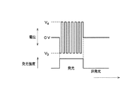
図6に、第二基板(3)の第一基板(2)に対する電位と、そのときのEC層(9)の発色/消色の状態の関連を示す。この図6に示されるように、例えば第二基板(3)の電位をV1(V1は、EC材料の負の値の還元電位)とすると、EC層中のEC材料が還元されて発色する。電圧の印加を停止した後も、EC材料はメモリ性を有することから発色した状態が継続する。また、第二基板(2)の電位をV2(V2は、EC材料の正の値の酸化電位)とすると、EC材料が酸化されて消色する。 FIG. 6 shows the relationship between the potential of the second substrate (3) with respect to the first substrate (2) and the color development / decoloration state of the EC layer (9) at that time. As shown in FIG. 6, for example, when the potential of the second substrate (3) is V 1 (V 1 is a reduction potential of a negative value of the EC material), the EC material in the EC layer is reduced and color develops. To do. Even after the application of the voltage is stopped, the EC material has a memory property, so that the colored state continues. When the potential of the second substrate (2) is V 2 (V 2 is an oxidation potential having a positive value of the EC material), the EC material is oxidized and decolored.
使用するEC材料によってはECL材料を含む電解質層中のイオンもこの反射表示のEC(酸化・還元)反応に関与する場合がある。例えば、WO3からなるEC層を適用した場合、ECL材料を含む電解質層中にLi+を含むもの(支持塩としてはLiCF3SO3等)を使用することが好ましい。 Depending on the EC material to be used, ions in the electrolyte layer containing the ECL material may also participate in the EC (oxidation / reduction) reaction of the reflection display. For example, when an EC layer made of WO 3 is applied, it is preferable to use an electrolyte layer containing ECL material containing Li + (such as LiCF 3 SO 3 as a supporting salt).
この場合のEC反応は下記(1)のように示すことができる。
WO3 + xe− + xLi+ ⇔ HxWO3 ・・・〔I〕
酸化反応(〔I〕式の左辺)では消色(透明)、還元反応(〔I〕式の右辺)では変色(青色)する。
The EC reaction in this case can be shown as (1) below.
WO 3 + xe - + xLi + ⇔ H x WO 3 ··· [I]
In the oxidation reaction (left side of the formula [I]), the color disappears (transparent), and in the reduction reaction (right side of the formula [I]), the color changes (blue).
ECLの発光を利用する図3の「発光・反射表示装置」において発光表示を行う際には、第二基板(3)には電圧を印加せず、第一基板(2)と第三基板(10)とに交流電圧を印加することができる。図7に、第一基板(2)の第三基板(10)に対する電位と、そのときの電解質溶液層(4)(ECL・電解質層)の発光/非発光の状態の関連を示す。第三基板(10)の第一基板(2)に対する電位は図示しないが、発光状態の期間中に、第一基板(2)と逆極性の電位になる。この図7に示されるように、例えば第一基板(2)電位がV3(V3は、ECL材料がアニオンラジカルになる負の値の還元電位)とV4(V4は、ECL材料がカチオンラジカルになる正の値の酸化電位)となるように交互に印加し、第三基板(10)にこれとは逆極性の電圧を印加すると、これらの第一基板(2)と第三基板(10)とで、交互にECL材料のアニオンラジカル、カチオンラジカルが生成し、これらが会合消失して、励起された発光材料が生成・失活により発光する。このような電圧を印加しなければ非発光状態となる。 When performing light emission display in the “light emitting / reflective display device” of FIG. 3 that uses light emission of ECL, no voltage is applied to the second substrate (3), and the first substrate (2) and the third substrate ( 10) and an alternating voltage can be applied. FIG. 7 shows the relationship between the potential of the first substrate (2) with respect to the third substrate (10) and the state of light emission / non-light emission of the electrolyte solution layer (4) (ECL / electrolyte layer) at that time. Although the potential of the third substrate (10) with respect to the first substrate (2) is not shown in the figure, the potential has a polarity opposite to that of the first substrate (2) during the light emitting state. As shown in FIG. 7, for example, the potential of the first substrate (2) is V 3 (V 3 is a negative reduction potential at which the ECL material becomes an anion radical) and V 4 (V 4 is the ECL material When the first substrate (2) and the third substrate are alternately applied so as to have a positive oxidation potential (which becomes a cation radical) and a voltage having a polarity opposite to that is applied to the third substrate (10). In (10), anion radicals and cation radicals of the ECL material are alternately generated, these are lost together, and the excited light emitting material emits light by generation / deactivation. If such a voltage is not applied, a non-light emitting state is obtained.
図3に示されるような「発光・反射表示装置」によれば、反射表示と発光表示の双方を1つの表示装置で行うことが可能となる。さらに、反射表示と発光表示とで、同種の電解質溶液を共通して用いることから、反射表示用のセルと発光表示用のセルを重ねることによる表示装置の大型化を防ぐことができる。さらに、画素を二分割して夫々の領域で反射表示と発光表示とを行う方式ではないため、画素領域を有効に活用することが出来る。 According to the “light emitting / reflective display device” as shown in FIG. 3, both the reflective display and the light emitting display can be performed by one display device. Furthermore, since the same type of electrolyte solution is used in common for the reflective display and the luminescent display, it is possible to prevent an increase in the size of the display device due to the overlapping of the reflective display cell and the luminescent display cell. Further, since the pixel is not divided into two parts and reflection display and light emission display are performed in each region, the pixel region can be used effectively.
<表示装置の製造>
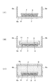
図1に示される本発明による表示装置は、例えば図8に示される手順(イ)→(ロ)→(ハ)に従って製造することが好ましい。すなわち、第一基板(2)が形成された基板(6a)に第二基板(3)が形成された支持基板(7)をスペーサ(8)等によって架設し(図8(イ))、次いで、基板(6a)と側壁部(6b)との空間を電解質溶液(11)で満たし(図8(ロ))、その後、底面部(6c)を設けて(図8(ハ))、基板(6a)と側壁(6b)と底面部(6c)とから形成された密閉セル(6)内に、第一基板(2)、第二基板(3)、電解質溶液層(4)および前記電解質溶液貯留部(5)を有する本発明による表示装置を製造することが好ましい。なお、密閉セル(6)に気泡などが封入されないように、特に電解質溶液の充填(図8(ロ))および密封セル作製作業(図8(ハ))は真空雰囲気下において実施することが好ましい。
<Manufacture of display devices>
The display device according to the present invention shown in FIG. 1 is preferably manufactured, for example, according to the procedure (A) → (B) → (C) shown in FIG. That is, the support substrate (7) on which the second substrate (3) is formed on the substrate (6a) on which the first substrate (2) is formed by a spacer (8) or the like (FIG. 8 (a)), and then The space between the substrate (6a) and the side wall (6b) is filled with the electrolyte solution (11) (FIG. 8 (b)), and then the bottom surface (6c) is provided (FIG. 8 (c)). 6a), a side wall (6b), and a bottom cell (6c), a closed cell (6) formed with a first substrate (2), a second substrate (3), an electrolyte solution layer (4) and the electrolyte solution It is preferable to manufacture a display device according to the invention having a reservoir (5). In order to prevent bubbles or the like from being enclosed in the sealed cell (6), it is particularly preferable that the electrolyte solution filling (FIG. 8 (b)) and the sealed cell manufacturing operation (FIG. 8 (c)) are performed in a vacuum atmosphere. .
また、本発明の図2の表示装置および図3の表示装置は、図8に示される手順に適当な改変を加えることによって容易に製造することができる。例えば、本発明の図2の表示装置は、図8の第二基板(3)の表面にEC層が形成されたものを使用することによって製造することができる。そして、本発明の図3の表示装置は、第一基板(2)および第三電極(10)が形成された基板(6a)を使用することによって容易に製造することができる。 Further, the display device of FIG. 2 and the display device of FIG. 3 of the present invention can be easily manufactured by appropriately modifying the procedure shown in FIG. For example, the display device of FIG. 2 of the present invention can be manufactured by using an EC layer formed on the surface of the second substrate (3) of FIG. And the display apparatus of FIG. 3 of this invention can be easily manufactured by using the board | substrate (6a) in which the 1st board | substrate (2) and the 3rd electrode (10) were formed.
図9(ロ)に示される高分子フィルムからなるフィルムパッケージを密封セルとする表示装置は、固定高分子フィルム(12)上に基板(6a)を接着剤層(13)によって固定し、この高分子フィルム(12)と他の前記高分子フィルム(14)とによって形成される空間内(図9(イ))に電解質溶液を満たし、その後、基板(6a)周辺部において高分子フィルム(12)と高分子フィルム(14)とを例えばヒートシール等によって接着することによって容易に製造することができる。 In a display device using a film package made of a polymer film shown in FIG. 9B as a sealed cell, a substrate (6a) is fixed on the fixed polymer film (12) by an adhesive layer (13). The space formed by the molecular film (12) and the other polymer film (14) (FIG. 9 (a)) is filled with the electrolyte solution, and then the polymer film (12) in the periphery of the substrate (6a). And a polymer film (14) can be easily manufactured by, for example, bonding them by heat sealing or the like.
以下、図面を参照して、具体例をさらに詳細に説明する。
<実施例1>
2.5インチ四方の表示装置を以下のように作製した。なお、各画素は単色の電気化学反応装置からなる図1に示す構成とし、1画素のサイズを100μm四方となるように作製した。
Hereinafter, specific examples will be described in more detail with reference to the drawings.
<Example 1>
A 2.5-inch square display device was produced as follows. Each pixel has the configuration shown in FIG. 1 composed of a monochromatic electrochemical reaction device, and the size of one pixel is 100 μm square.
まず、基板(6a)として厚さ0.7mmのガラスからなる基板を用い、膜厚1000ÅのITO(Indium Tin Oxide)をスパッタにより形成し、パターニングして第一基板(2)とした。支持基板(7)として厚さ0.7mmのガラス基板を用い、厚さ1000ÅのAg膜を形成してパターニングし、第二基板(3)を形成した。 First, a substrate made of glass having a thickness of 0.7 mm was used as the substrate (6a), and ITO (Indium Tin Oxide) having a thickness of 1000 mm was formed by sputtering and patterned to obtain a first substrate (2). A glass substrate having a thickness of 0.7 mm was used as the supporting substrate (7), and an Ag film having a thickness of 1000 mm was formed and patterned to form a second substrate (3).
N2バブリングを行いながら10mMのルブレンを1,2−ジメトキシエタン中に添加して、ECL分子含有電解質溶液を調製した。 While performing N 2 bubbling, 10 mM rubrene was added into 1,2-dimethoxyethane to prepare an ECL molecule-containing electrolyte solution.
基板(6a)と支持基板(7)とを10μmの接着スペーサー(8)を介して、両基板間が10μmギャップとなるよう対向配置した。また、さらに基板(6a)の周辺部に100μmの側壁部(6b)を形成した。真空下でECL分子含有電解質溶液を支持基板(7)の上方から滴下し、底面部(6c)を貼り合わせた。 The substrate (6a) and the supporting substrate (7) were arranged to face each other with a 10 μm gap between them through a 10 μm adhesive spacer (8). Further, a side wall (6b) having a thickness of 100 μm was formed on the periphery of the substrate (6a). Under vacuum, the ECL molecule-containing electrolyte solution was dropped from above the support substrate (7), and the bottom surface portion (6c) was bonded.
第一基板(2)と第二基板(3)間に12VのDC電圧を印加すると、黄色の発光が観測された。 When a DC voltage of 12 V was applied between the first substrate (2) and the second substrate (3), yellow light emission was observed.
<実施例2>
2.5インチ四方の表示装置を以下のように作製した。なお、各画素は単色の電気化学反応装置からなる図1に示す構成とし、1画素のサイズを100μm四方となるように作製した。
<Example 2>
A 2.5-inch square display device was produced as follows. Each pixel has the configuration shown in FIG. 1 composed of a monochromatic electrochemical reaction device, and the size of one pixel is 100 μm square.
まず、基板(6a)として厚さ0.7mmのガラスからなる基板を用い、膜厚1000ÅのITOをスパッタにより形成し、パターニングして第一基板(2)とした。 First, a substrate made of glass having a thickness of 0.7 mm was used as the substrate (6a), ITO having a thickness of 1000 mm was formed by sputtering, and patterned to obtain a first substrate (2).
支持基板(7)として厚さ0.7mmのガラス基板を用い、厚さ1000ÅのITO膜を形成してパターニングし、第二基板(3)を形成した。また、第二基板(3)の背面には反射層用のAl膜を形成しさらにSiO2やポリイミド等の無機または有機の保護膜を形成した。第二基板(3)を形成した支持基板(7)の表面にEB蒸着によってEC層(WO3膜)(9)約1000Åを形成した。 A glass substrate having a thickness of 0.7 mm was used as the support substrate (7), and an ITO film having a thickness of 1000 mm was formed and patterned to form a second substrate (3). Further, an Al film for a reflective layer was formed on the back surface of the second substrate (3), and an inorganic or organic protective film such as SiO 2 or polyimide was further formed. An EC layer (WO 3 film) (9) of about 1000 mm was formed on the surface of the support substrate (7) on which the second substrate (3) was formed by EB vapor deposition.
N2バブリングを行いながら100mMのLiClO4をプロピレンカーボネート中に添加して、電解質溶液を調製した。 An electrolyte solution was prepared by adding 100 mM LiClO 4 into propylene carbonate with N 2 bubbling.
基板(6a)と支持基板(7)とをスペーサー(8)を介して、両基板間が10μmギャップとなるよう対向配置した。また、さらに基板(6a)の周辺部に100μmの側壁(6b)を形成した。真空下で電解質溶液を支持基板(7)の上方から滴下し、底面部(6c)を貼り合わせた。 The substrate (6a) and the support substrate (7) were arranged to face each other with a 10 μm gap between the two substrates via the spacer (8). Further, a 100 μm side wall (6b) was formed on the periphery of the substrate (6a). The electrolyte solution was dropped from above the support substrate (7) under vacuum, and the bottom surface portion (6c) was bonded.
第一基板(2)と第二基板(3)間に2.5VのDC電圧を印加すると、濃青色の発色が観測された。 When a DC voltage of 2.5 V was applied between the first substrate (2) and the second substrate (3), dark blue color was observed.
<実施例3>
2.5インチ四方の表示装置を以下のように作製した。なお、各画素は単色の電気化学反応装置からなる図3に示す構成とし、1画素のサイズを100μm四方となるように作製した。
<Example 3>
A 2.5-inch square display device was produced as follows. Each pixel has a configuration shown in FIG. 3 composed of a single-color electrochemical reaction device, and the size of one pixel is 100 μm square.
まず、基板(6a)として厚さ0.7mmのガラスからなる基板を用い、膜厚1000ÅのITO をスパッタにより形成し、パターニングして第一基板(2)および第三基板(10)とした。 First, a substrate made of glass having a thickness of 0.7 mm was used as the substrate (6a), ITO having a thickness of 1000 mm was formed by sputtering, and patterned to obtain a first substrate (2) and a third substrate (10).
支持基板(7)としてガラス基板を用い、厚さ1000ÅのITO膜を形成してパターニングし、第二基板(3)を形成した。 A glass substrate was used as the support substrate (7), and an ITO film having a thickness of 1000 mm was formed and patterned to form a second substrate (3).
第二基板(3)を形成した支持基板(7)上に電解重合によってEC層(ポリピロール膜)約1200Åを形成した。 On the support substrate (7) on which the second substrate (3) was formed, an EC layer (polypyrrole film) of about 1200 mm was formed by electrolytic polymerization.
N2バブリングを行いながら100mMのLiCF3SO3を支持塩としてDMF(N,N−ジメチルホルムアミド)溶媒に溶解させたものに、8mMのRu(bpy)3Cl2(Tris(2,2’−bipyridine) ruthenium (II) chloride)をECL材料として溶解させて、電解質溶液を調製した。 To a solution of 100 mM LiCF 3 SO 3 dissolved in DMF (N, N-dimethylformamide) solvent as a supporting salt while performing N 2 bubbling, 8 mM Ru (bpy) 3 Cl 2 (Tris (2,2′- bipyridine) ruthenium (II) chloride) was dissolved as an ECL material to prepare an electrolyte solution.
基板(6a)と支持基板(7)とをスペーサー(8)を介して、両基板間が10μmギャップとなるよう対向配置した。また、さらに基板(6a)の周辺部に100μmの側壁部(6b)を形成した。真空下でこの電解質溶液を支持基板(7)の上方から滴下し、底面部(6c)を貼り合わせた。 The substrate (6a) and the support substrate (7) were arranged to face each other with a 10 μm gap between the two substrates via the spacer (8). Further, a side wall (6b) having a thickness of 100 μm was formed on the periphery of the substrate (6a). This electrolyte solution was dropped from above the support substrate (7) under vacuum, and the bottom surface portion (6c) was bonded.
第一基板(2)と第三基板(10)とを同電位とし、参照電極に対して第二基板(3)の電位が+1.5V、−2Vとなるように電圧を印加した。すると、消色状態(+1.5V)と青色の着色状態(−2V)を実現し、反射表示が可能であることがわかった。 The first substrate (2) and the third substrate (10) were set to the same potential, and a voltage was applied so that the potential of the second substrate (3) was + 1.5V and −2V with respect to the reference electrode. Then, it turned out that a decoloring state (+ 1.5V) and a blue coloring state (-2V) are implement | achieved and a reflective display is possible.
また、第二基板(3)には電圧を印加せず、第一基板(2)と第三基板(10)との間に電位差が10Vとなるよう、10Hzの交流電流を印加すると、オレンジ色の発光が観測された。 When no voltage is applied to the second substrate (3) and an alternating current of 10 Hz is applied so that the potential difference is 10 V between the first substrate (2) and the third substrate (10), the orange color Was observed.
1 表示装置
2 第一基板
3 第二基板
4 電解質溶液層
5 電解質溶液貯留部
DESCRIPTION OF
Claims (9)
Priority Applications (1)
| Application Number | Priority Date | Filing Date | Title |
|---|---|---|---|
| JP2004103916A JP4257251B2 (en) | 2004-03-31 | 2004-03-31 | Display device |
Applications Claiming Priority (1)
| Application Number | Priority Date | Filing Date | Title |
|---|---|---|---|
| JP2004103916A JP4257251B2 (en) | 2004-03-31 | 2004-03-31 | Display device |
Publications (2)
| Publication Number | Publication Date |
|---|---|
| JP2005292258A true JP2005292258A (en) | 2005-10-20 |
| JP4257251B2 JP4257251B2 (en) | 2009-04-22 |
Family
ID=35325288
Family Applications (1)
| Application Number | Title | Priority Date | Filing Date |
|---|---|---|---|
| JP2004103916A Expired - Fee Related JP4257251B2 (en) | 2004-03-31 | 2004-03-31 | Display device |
Country Status (1)
| Country | Link |
|---|---|
| JP (1) | JP4257251B2 (en) |
Cited By (6)
| Publication number | Priority date | Publication date | Assignee | Title |
|---|---|---|---|---|
| JP2007256386A (en) * | 2006-03-20 | 2007-10-04 | Niigata Univ | All-solid-state electrochromic device, electrochromic film and manufacturing method thereof |
| JP2007322824A (en) * | 2006-06-01 | 2007-12-13 | Fuji Xerox Co Ltd | Image display medium |
| US7981526B2 (en) * | 2008-03-25 | 2011-07-19 | Kabushiki Kaisha Toshiba | Display device |
| US8120245B2 (en) | 2008-04-15 | 2012-02-21 | University Of Florida Research Foundation, Inc. | Interdigitated electrode dual electroemissive/electrochromic devices |
| WO2013129208A1 (en) * | 2012-02-28 | 2013-09-06 | 国立大学法人九州大学 | Method for producing light-emitting device using liquid light-emitting material, and light-emitting device using liquid light-emitting material |
| CN114149799A (en) * | 2021-12-03 | 2022-03-08 | 燕山大学 | Method for preparing electrochemiluminescence solution, electrochemiluminescence device and application thereof |
-
2004
- 2004-03-31 JP JP2004103916A patent/JP4257251B2/en not_active Expired - Fee Related
Cited By (7)
| Publication number | Priority date | Publication date | Assignee | Title |
|---|---|---|---|---|
| JP2007256386A (en) * | 2006-03-20 | 2007-10-04 | Niigata Univ | All-solid-state electrochromic device, electrochromic film and manufacturing method thereof |
| JP2007322824A (en) * | 2006-06-01 | 2007-12-13 | Fuji Xerox Co Ltd | Image display medium |
| US7981526B2 (en) * | 2008-03-25 | 2011-07-19 | Kabushiki Kaisha Toshiba | Display device |
| US8120245B2 (en) | 2008-04-15 | 2012-02-21 | University Of Florida Research Foundation, Inc. | Interdigitated electrode dual electroemissive/electrochromic devices |
| WO2013129208A1 (en) * | 2012-02-28 | 2013-09-06 | 国立大学法人九州大学 | Method for producing light-emitting device using liquid light-emitting material, and light-emitting device using liquid light-emitting material |
| CN114149799A (en) * | 2021-12-03 | 2022-03-08 | 燕山大学 | Method for preparing electrochemiluminescence solution, electrochemiluminescence device and application thereof |
| CN114149799B (en) * | 2021-12-03 | 2024-01-23 | 燕山大学 | Preparation method of electrochemiluminescence solution, electrochemiluminescence device and application thereof |
Also Published As
| Publication number | Publication date |
|---|---|
| JP4257251B2 (en) | 2009-04-22 |
Similar Documents
| Publication | Publication Date | Title |
|---|---|---|
| JP4060779B2 (en) | Display device | |
| JP4384005B2 (en) | Display device | |
| Mortimer | Electrochromic materials | |
| US20070109218A1 (en) | Display apparatus and display element driving method | |
| JP5648805B2 (en) | Electrochromic display element | |
| JP2011191588A (en) | Electrochromic display device and method of manufacturing the same | |
| JP2008116718A (en) | Electrochromic device | |
| CA3170900A1 (en) | Electrochromic device and method for producing the same | |
| JP2009230073A (en) | Display | |
| JP2012155017A (en) | Driving method of electrochromic display device and display device | |
| US7888853B2 (en) | Light-emitting device exhibiting electrochemical luminescence | |
| JP4257251B2 (en) | Display device | |
| US20070257263A1 (en) | Display device | |
| JP2004020928A (en) | Electrochromic display element, method of manufacturing the same, and electrochromic display device | |
| JP4568157B2 (en) | Display device | |
| JP2008111941A (en) | Electrochromic device | |
| JP4550679B2 (en) | Display device | |
| JP5023450B2 (en) | Electrochromic device and display method using the same | |
| US20070040499A1 (en) | Light emitting device, display device and method of fabricating the same | |
| JP4765547B2 (en) | Electrochromic device | |
| JP2011017873A (en) | Electrochromic display device and driving method therefor | |
| JP2007047656A (en) | Electrochromic device and display method using the same | |
| JP4899719B2 (en) | Electrochromic device | |
| JP2004286976A (en) | Color rewritable display device using electrochromic material, and method for manufacturing same | |
| JP2008145598A (en) | Electrochromic device |
Legal Events
| Date | Code | Title | Description |
|---|---|---|---|
| A131 | Notification of reasons for refusal |
Free format text: JAPANESE INTERMEDIATE CODE: A131 Effective date: 20080418 |
|
| A521 | Request for written amendment filed |
Free format text: JAPANESE INTERMEDIATE CODE: A523 Effective date: 20080617 |
|
| TRDD | Decision of grant or rejection written | ||
| A01 | Written decision to grant a patent or to grant a registration (utility model) |
Free format text: JAPANESE INTERMEDIATE CODE: A01 Effective date: 20090127 |
|
| A01 | Written decision to grant a patent or to grant a registration (utility model) |
Free format text: JAPANESE INTERMEDIATE CODE: A01 |
|
| A61 | First payment of annual fees (during grant procedure) |
Free format text: JAPANESE INTERMEDIATE CODE: A61 Effective date: 20090202 |
|
| FPAY | Renewal fee payment (event date is renewal date of database) |
Free format text: PAYMENT UNTIL: 20120206 Year of fee payment: 3 |
|
| FPAY | Renewal fee payment (event date is renewal date of database) |
Free format text: PAYMENT UNTIL: 20120206 Year of fee payment: 3 |
|
| FPAY | Renewal fee payment (event date is renewal date of database) |
Free format text: PAYMENT UNTIL: 20120206 Year of fee payment: 3 |
|
| FPAY | Renewal fee payment (event date is renewal date of database) |
Free format text: PAYMENT UNTIL: 20130206 Year of fee payment: 4 |
|
| FPAY | Renewal fee payment (event date is renewal date of database) |
Free format text: PAYMENT UNTIL: 20140206 Year of fee payment: 5 |
|
| LAPS | Cancellation because of no payment of annual fees |