JP2005291927A - Sensor - Google Patents
Sensor Download PDFInfo
- Publication number
- JP2005291927A JP2005291927A JP2004107606A JP2004107606A JP2005291927A JP 2005291927 A JP2005291927 A JP 2005291927A JP 2004107606 A JP2004107606 A JP 2004107606A JP 2004107606 A JP2004107606 A JP 2004107606A JP 2005291927 A JP2005291927 A JP 2005291927A
- Authority
- JP
- Japan
- Prior art keywords
- sensor
- signal
- sensor element
- change
- phase
- Prior art date
- Legal status (The legal status is an assumption and is not a legal conclusion. Google has not performed a legal analysis and makes no representation as to the accuracy of the status listed.)
- Pending
Links
- 230000008859 change Effects 0.000 claims abstract description 145
- 238000001514 detection method Methods 0.000 claims abstract description 126
- 229920000049 Carbon (fiber) Polymers 0.000 claims abstract description 33
- 239000004917 carbon fiber Substances 0.000 claims abstract description 33
- 230000010355 oscillation Effects 0.000 claims description 51
- 239000000835 fiber Substances 0.000 claims description 21
- 230000001629 suppression Effects 0.000 claims 1
- 239000012071 phase Substances 0.000 description 154
- VNWKTOKETHGBQD-UHFFFAOYSA-N methane Chemical compound C VNWKTOKETHGBQD-UHFFFAOYSA-N 0.000 description 20
- 230000003247 decreasing effect Effects 0.000 description 10
- 239000003990 capacitor Substances 0.000 description 7
- 238000010586 diagram Methods 0.000 description 7
- 230000010363 phase shift Effects 0.000 description 7
- 230000000694 effects Effects 0.000 description 5
- 238000004519 manufacturing process Methods 0.000 description 5
- 230000007423 decrease Effects 0.000 description 4
- 239000002134 carbon nanofiber Substances 0.000 description 3
- 238000000034 method Methods 0.000 description 3
- 230000004044 response Effects 0.000 description 3
- 230000035945 sensitivity Effects 0.000 description 3
- 230000008878 coupling Effects 0.000 description 2
- 238000010168 coupling process Methods 0.000 description 2
- 238000005859 coupling reaction Methods 0.000 description 2
- 230000001934 delay Effects 0.000 description 2
- 230000003111 delayed effect Effects 0.000 description 2
- 239000000203 mixture Substances 0.000 description 2
- 239000000843 powder Substances 0.000 description 2
- MTPVUVINMAGMJL-UHFFFAOYSA-N trimethyl(1,1,2,2,2-pentafluoroethyl)silane Chemical compound C[Si](C)(C)C(F)(F)C(F)(F)F MTPVUVINMAGMJL-UHFFFAOYSA-N 0.000 description 2
- OKTJSMMVPCPJKN-UHFFFAOYSA-N Carbon Chemical compound [C] OKTJSMMVPCPJKN-UHFFFAOYSA-N 0.000 description 1
- RYGMFSIKBFXOCR-UHFFFAOYSA-N Copper Chemical compound [Cu] RYGMFSIKBFXOCR-UHFFFAOYSA-N 0.000 description 1
- GWEVSGVZZGPLCZ-UHFFFAOYSA-N Titan oxide Chemical compound O=[Ti]=O GWEVSGVZZGPLCZ-UHFFFAOYSA-N 0.000 description 1
- NRTOMJZYCJJWKI-UHFFFAOYSA-N Titanium nitride Chemical compound [Ti]#N NRTOMJZYCJJWKI-UHFFFAOYSA-N 0.000 description 1
- XLOMVQKBTHCTTD-UHFFFAOYSA-N Zinc monoxide Chemical compound [Zn]=O XLOMVQKBTHCTTD-UHFFFAOYSA-N 0.000 description 1
- 230000001133 acceleration Effects 0.000 description 1
- 239000000956 alloy Substances 0.000 description 1
- HSFWRNGVRCDJHI-UHFFFAOYSA-N alpha-acetylene Natural products C#C HSFWRNGVRCDJHI-UHFFFAOYSA-N 0.000 description 1
- 229910003481 amorphous carbon Inorganic materials 0.000 description 1
- 230000003321 amplification Effects 0.000 description 1
- 229910002113 barium titanate Inorganic materials 0.000 description 1
- JRPBQTZRNDNNOP-UHFFFAOYSA-N barium titanate Chemical compound [Ba+2].[Ba+2].[O-][Ti]([O-])([O-])[O-] JRPBQTZRNDNNOP-UHFFFAOYSA-N 0.000 description 1
- 238000005452 bending Methods 0.000 description 1
- 230000008901 benefit Effects 0.000 description 1
- 239000002041 carbon nanotube Substances 0.000 description 1
- 229910021393 carbon nanotube Inorganic materials 0.000 description 1
- 239000011304 carbon pitch Substances 0.000 description 1
- 239000003575 carbonaceous material Substances 0.000 description 1
- 239000004020 conductor Substances 0.000 description 1
- 229910052802 copper Inorganic materials 0.000 description 1
- 239000010949 copper Substances 0.000 description 1
- 239000013078 crystal Substances 0.000 description 1
- NKZSPGSOXYXWQA-UHFFFAOYSA-N dioxido(oxo)titanium;lead(2+) Chemical compound [Pb+2].[O-][Ti]([O-])=O NKZSPGSOXYXWQA-UHFFFAOYSA-N 0.000 description 1
- 238000006073 displacement reaction Methods 0.000 description 1
- 238000002474 experimental method Methods 0.000 description 1
- 230000001939 inductive effect Effects 0.000 description 1
- 229910052451 lead zirconate titanate Inorganic materials 0.000 description 1
- HFGPZNIAWCZYJU-UHFFFAOYSA-N lead zirconate titanate Chemical compound [O-2].[O-2].[O-2].[O-2].[O-2].[Ti+4].[Zr+4].[Pb+2] HFGPZNIAWCZYJU-UHFFFAOYSA-N 0.000 description 1
- 238000005259 measurement Methods 0.000 description 1
- 239000007769 metal material Substances 0.000 description 1
- 238000003199 nucleic acid amplification method Methods 0.000 description 1
- 230000003287 optical effect Effects 0.000 description 1
- 239000011295 pitch Substances 0.000 description 1
- 229920001197 polyacetylene Polymers 0.000 description 1
- 239000002861 polymer material Substances 0.000 description 1
- 238000003825 pressing Methods 0.000 description 1
- 229920002050 silicone resin Polymers 0.000 description 1
- 229910052709 silver Inorganic materials 0.000 description 1
- 239000004332 silver Substances 0.000 description 1
- 238000001947 vapour-phase growth Methods 0.000 description 1
- 229910000859 α-Fe Inorganic materials 0.000 description 1
Images
Landscapes
- Measurement Of Length, Angles, Or The Like Using Electric Or Magnetic Means (AREA)
Abstract
Description
本発明は、例えばセンサ素子に加わった応力や電磁波等の被検出量を検出するセンサに関するものである。 The present invention relates to a sensor for detecting a detected amount such as stress or electromagnetic wave applied to a sensor element, for example.
従来、例えば、物体に加わった応力を検出するために歪ゲージ(例えば、特許文献1参照)が用いられている。歪ゲージは、同歪ゲージが固着された物体に加わる応力に比例してその抵抗値が変化するセンサ素子である。歪ゲージを用いたセンサは、この歪ゲージの抵抗値の変化を電圧値の変化として検出することにより、物体に加わった応力を検出することができる。また、磁界の変化を検出するためには、例えば磁気抵抗素子(MRE)を用いたセンサ(例えば、特許文献2参照)が使用されている。磁気抵抗素子は、その周囲の磁界の強度に比例してその抵抗値が変化するセンサ素子である。磁気抵抗素子を用いたセンサは、この磁気抵抗素子の抵抗値の変化を電圧値の変化として検出することにより、センサ周囲の磁界の強度を検出することができる。そして、これらセンサにより検出された応力や電磁波等の物理量(被検出量)は、例えばロボット等の制御対象を制御するための制御情報に用いられている。
近年、被検出量の微小な変化の検出を目的として、更に高感度なセンサの提供が望まれている。しかしながら、従来のセンサでは、センサ素子が有する電気的な特性(例えば、応力に対する抵抗変化の直線性)等から、被検出量の微小な変化を正確に検出できるとはいい難かった。 In recent years, it has been desired to provide a sensor with higher sensitivity for the purpose of detecting minute changes in the amount to be detected. However, in the conventional sensor, it is difficult to accurately detect a minute change in the amount to be detected from the electrical characteristics of the sensor element (for example, linearity of resistance change with respect to stress).
本発明は、こうした実情に鑑みてなされたものであり、その目的は、センサの被検出量の微小な変化を検出することができるセンサを提供することにある。 The present invention has been made in view of such circumstances, and an object of the present invention is to provide a sensor that can detect a minute change in the detected amount of the sensor.
上記課題を解決するために請求項1に記載の発明では、太さがμm単位以下の寸法に形成されたコイル形状をなす炭素繊維が誘電性の媒体中に分散されることにより構成されるセンサ素子と、前記センサ素子に基準信号を出力する基準信号入力手段と、前記基準信号の入力に対する前記センサ素子の抵抗成分及びリアクタンス成分のうち少なくとも一方の変化に基づくセンサ出力信号を検出する検出手段とを備えることを要旨とする。
In order to solve the above-mentioned problem, in the invention according to
請求項2に記載の発明では、請求項1に記載のセンサにおいて、前記基準信号は、時間の経過とともに振幅が変化する交流信号であり、前記検出手段は、前記基準信号に基づく検波基準信号を用いて前記センサ出力信号を検波することを要旨とする。 According to a second aspect of the present invention, in the sensor according to the first aspect, the reference signal is an AC signal whose amplitude changes with the passage of time, and the detection means generates a detection reference signal based on the reference signal. The gist is to detect the sensor output signal by using the sensor.
請求項3に記載の発明では、請求項2に記載のセンサにおいて、前記検出手段は、前記検波基準信号の振幅及び位相のうち少なくとも一方を調整する信号調整手段を備えることを要旨とする。 According to a third aspect of the present invention, there is provided a sensor according to the second aspect, wherein the detecting means includes a signal adjusting means for adjusting at least one of an amplitude and a phase of the detection reference signal.
請求項4に記載の発明では、請求項3に記載のセンサにおいて、前記信号調整手段は、前記検波基準信号を移相させることにより、前記センサ素子の抵抗成分及びリアクタンス成分が変化しない状態における前記センサ出力信号に前記検波基準信号の位相を一致させる移相器を備えることを要旨とする。 According to a fourth aspect of the present invention, in the sensor according to the third aspect, the signal adjusting means shifts the phase of the detection reference signal so that the resistance component and reactance component of the sensor element do not change. The gist is to provide a phase shifter for matching the phase of the detection reference signal to the sensor output signal.
請求項5に記載の発明では、請求項3または請求項4に記載のセンサにおいて、前記検出手段は、前記検波基準信号と前記センサ出力信号とを比較することにより前記センサ出力信号を検波し、両信号間の位相差を検出することを要旨とする。
In the invention according to claim 5, in the sensor according to
請求項6に記載の発明では、請求項3または請求項4に記載のセンサにおいて、前記信号調整手段は、前記センサ素子の抵抗成分及びリアクタンス成分が変化しない状態における前記センサ出力信号に対して90°の位相差となるように前記検波基準信号を移相させて、直交信号を生成する直交用移相器を備え、前記検出手段は、前記検波基準信号を用いて前記センサ出力信号を検波する第1検波器と、前記直交信号を用いて前記センサ出力信号を検波する第2検波器とを備えることを要旨とする。 According to a sixth aspect of the present invention, in the sensor according to the third or fourth aspect, the signal adjustment unit is configured to perform 90 with respect to the sensor output signal in a state where the resistance component and reactance component of the sensor element do not change. A phase shifter for quadrature that generates a quadrature signal by shifting the phase of the detection reference signal so as to obtain a phase difference of °, and the detection means detects the sensor output signal using the detection reference signal The gist includes a first detector and a second detector that detects the sensor output signal using the orthogonal signal.
請求項7に記載の発明では、請求項1に記載のセンサにおいて、前記基準信号入力手段と前記センサ素子とは、該センサ素子のリアクタンス成分の変化により周波数が変動し、該センサ素子の抵抗成分の変化により振幅が変動する発振信号を出力する発振部を構成し、前記検出手段は、前記発振信号の周波数及び振幅のうち少なくとも一方を検出することを要旨とする。 According to a seventh aspect of the present invention, in the sensor according to the first aspect, the reference signal input means and the sensor element vary in frequency due to a change in a reactance component of the sensor element, and a resistance component of the sensor element An oscillating unit that outputs an oscillating signal whose amplitude fluctuates due to a change in frequency is configured, and the detecting means detects at least one of the frequency and amplitude of the oscillating signal.
請求項8に記載の発明では、請求項7に記載の発明において、前記基準信号入力手段は、前記発振信号の周波数を変化させるリアクタンス調整手段を備え、前記発振信号の周波数を変化させる旨の制御信号が入力された際には前記リアクタンス調整手段により前記発振信号の周波数を調整し、前記検出手段は、前記発振信号の周波数の変化量を検出する位相検波器を備え、該変化量を前記センサ素子におけるリアクタンス成分の変化として検出するとともに、該変化量に基づいて該周波数の変化を抑制するべく前記制御信号を出力することを要旨とする。
The invention according to claim 8 is the control according to
請求項9に記載の発明では、太さがμm単位以下の寸法に形成された弾力性を有する導電性繊維が誘電性の媒体中に分散されることにより構成されるセンサ素子と、前記センサ素子に基準信号を出力する基準信号入力手段と、前記基準信号の入力に対する前記センサ素子の抵抗成分及びリアクタンス成分のうち少なくとも一方の変化に基づくセンサ出力信号を検出する検出手段とを備えることを要旨とする。 According to a ninth aspect of the present invention, there is provided a sensor element configured by dispersing elastic conductive fibers having a thickness of a size of μm or less in a dielectric medium, and the sensor element And a reference signal input means for outputting a reference signal to the reference signal and a detection means for detecting a sensor output signal based on a change in at least one of a resistance component and a reactance component of the sensor element with respect to the input of the reference signal. To do.
請求項10に記載の発明では、抵抗成分及びリアクタンス成分を有し、被検出量の変化に基づいて抵抗成分及びリアクタンス成分のうち少なくとも一方が変化するセンサ素子と、前記センサ素子に交流信号を出力する基準信号入力手段と、前記センサ素子の抵抗成分及びリアクタンス成分が変化しない状態において、前記交流信号の入力に対する前記センサ素子の抵抗成分及びリアクタンス成分のうち少なくとも一方の変化に基づくセンサ出力信号に対して90°の位相差となるように前記交流信号を移相させて、直交信号を生成する直交用移相器を備え、前記交流信号に基づく検波基準信号を用いて前記センサ出力信号を検波する第1検波器と、前記直交信号を用いて前記センサ出力信号を検波する第2検波器とを備えることを要旨とする。 In a tenth aspect of the present invention, a sensor element having a resistance component and a reactance component, and at least one of the resistance component and the reactance component changes based on a change in the detected amount, and an AC signal is output to the sensor element. And a sensor output signal based on a change in at least one of the resistance component and reactance component of the sensor element with respect to the input of the AC signal in a state where the resistance component and reactance component of the sensor element do not change. A phase shifter for quadrature that generates a quadrature signal by shifting the phase of the ac signal so that the phase difference is 90 °, and detects the sensor output signal using a detection reference signal based on the ac signal. The gist includes a first detector and a second detector that detects the sensor output signal using the orthogonal signal.
以下、本発明の作用について説明する。
請求項1に記載の発明によれば、センサ素子は、コイル形状をなす炭素繊維が誘電性の媒体中に分散されることにより構成されている。このため、センサ素子は、電気的特性として抵抗成分とリアクタンス成分とを有する。しかも、センサ素子を構成する炭素繊維は非常に小さなコイル状に形成されている。このため、センサ素子に外力(本明細書においては、応力等の機械的な力、及び電磁波等の電気的な力の総称として用いる)が加わると、その外力の微小な変位や変動にも応答して、該センサ素子の抵抗成分及びリアクタンス成分のうち少なくとも一方が変化する。センサ出力信号は、これら変化に基づいて定まることから、センサ素子に加わる外力の微小な変化に応答して変化する。検出手段は、こうしたセンサ出力信号を検出するため、センサ素子に加わる外力の微小な変化を検出することができる。すなわち、検出手段はセンサ素子の被検出量の微小な変化を検出することができる。
The operation of the present invention will be described below.
According to the first aspect of the present invention, the sensor element is configured by dispersing carbon fibers having a coil shape in a dielectric medium. For this reason, the sensor element has a resistance component and a reactance component as electrical characteristics. And the carbon fiber which comprises a sensor element is formed in the very small coil shape. For this reason, when an external force (used in this specification as a general term for mechanical force such as stress and electric force such as electromagnetic wave) is applied to the sensor element, it responds to minute displacement and fluctuation of the external force. Thus, at least one of the resistance component and the reactance component of the sensor element changes. Since the sensor output signal is determined based on these changes, it changes in response to a minute change in the external force applied to the sensor element. Since the detection means detects such a sensor output signal, it can detect a minute change in the external force applied to the sensor element. That is, the detection means can detect a minute change in the detected amount of the sensor element.
請求項2に記載の発明によれば、基準信号は、時間の経過とともに振幅が変化する交流信号である。このため、センサ素子において抵抗成分が変化した場合には、基準信号に対してセンサ出力信号の振幅が変化し、センサ素子においてリアクタンス成分が変化した場合には、検波基準信号とセンサ出力信号との間に位相差が生じる。検出手段は、検波基準信号を用いてセンサ出力信号を検波するため、センサ出力信号の振幅の変化からセンサ素子における抵抗成分の変化を検出し、検波基準信号とセンサ出力信号との位相差の変化からセンサ素子におけるリアクタンス成分の変化を検出することが可能となる。つまり、検出手段は、センサ素子における抵抗成分の変化、及びリアクタンス成分の変化のうち少なくとも一方を検出することが可能となる。したがって、例えば抵抗成分の変化とリアクタンス成分の変化とが検出手段によって総合的に検出されるようにすれば、被検出量の微小な変化が確実に検出され、センサの感度を向上させることができる。 According to the second aspect of the present invention, the reference signal is an AC signal whose amplitude changes with time. For this reason, when the resistance component changes in the sensor element, the amplitude of the sensor output signal changes with respect to the reference signal, and when the reactance component changes in the sensor element, the detection reference signal and the sensor output signal There is a phase difference between them. Since the detection means detects the sensor output signal using the detection reference signal, the detection means detects the change in the resistance component in the sensor element from the change in the amplitude of the sensor output signal, and the change in the phase difference between the detection reference signal and the sensor output signal Therefore, it is possible to detect a change in reactance component in the sensor element. That is, the detection means can detect at least one of a change in resistance component and a change in reactance component in the sensor element. Therefore, for example, if a change in the resistance component and a change in the reactance component are comprehensively detected by the detection means, a minute change in the detected amount can be reliably detected, and the sensitivity of the sensor can be improved. .
請求項3に記載の発明によれば、信号調整手段は、検波基準信号の振幅及び位相のうち少なくとも一方を調整する。このため、例えば、センサ素子に外力が加わっていない状態におけるセンサ出力信号に検波基準信号の振幅や位相を一致させることができる。一般に、検出手段に入力されるセンサ出力信号は、基準信号に対して回路構成上の遅れが生じる場合がある。よって、例えば両信号の位相を一致させるようにすれば、回路の構成上生じる遅延成分等が排除され、被検出量の微小な変化を正確に検出することができる。
According to the invention described in
請求項4に記載の発明によれば、センサ素子の抵抗成分及びリアクタンス成分が変化しない状態におけるセンサ出力信号の位相と検波基準信号の位相とが一致する。このため、回路の構成上生じる遅延成分等が排除され、被検出量の微小な変化を正確に検出することができる。 According to the fourth aspect of the present invention, the phase of the sensor output signal and the phase of the detection reference signal coincide with each other when the resistance component and reactance component of the sensor element do not change. For this reason, a delay component or the like generated in the circuit configuration is eliminated, and a minute change in the detected amount can be accurately detected.
請求項5に記載の発明によれば、検出手段は、検波基準信号とセンサ出力信号とを比較して、両信号の位相差を検出する。よって、両信号の位相差から、センサ素子におけるリアクタンス成分の変化を検出することができる。したがって、センサ素子のリアクタンス成分を変化させる外力の微小な変化を検出することができる。 According to the invention described in claim 5, the detecting means compares the detection reference signal with the sensor output signal and detects the phase difference between the two signals. Therefore, a change in reactance component in the sensor element can be detected from the phase difference between the two signals. Therefore, a minute change in external force that changes the reactance component of the sensor element can be detected.
請求項6に記載の発明によれば、検出手段は、いわゆる直交検波方式によりセンサ出力信号を検波する。このため、第1検波器から出力される信号と第2検波器から出力される信号とに基づいて、同相信号に対するセンサ出力信号の位相の変化及び同相信号に対するセンサ出力信号の振幅の変化を求めることができる。センサ出力信号の位相の変化は、センサ素子におけるリアクタンス成分の変化に、センサ出力信号の振幅の変化は、センサ素子における抵抗成分の変化にそれぞれ相当する。よって、センサ素子における抵抗成分の変化及びリアクタンス成分の変化をそれぞれ求めることができる。したがって、被検出量の変化を総合的に検出することができ、センサの感度を向上させることができる。 According to the invention described in claim 6, the detection means detects the sensor output signal by a so-called quadrature detection method. Therefore, based on the signal output from the first detector and the signal output from the second detector, the change in the phase of the sensor output signal with respect to the in-phase signal and the change in the amplitude of the sensor output signal with respect to the in-phase signal Can be requested. A change in phase of the sensor output signal corresponds to a change in reactance component in the sensor element, and a change in amplitude of the sensor output signal corresponds to a change in resistance component in the sensor element. Accordingly, it is possible to obtain a change in resistance component and a change in reactance component in the sensor element. Therefore, changes in the amount to be detected can be comprehensively detected, and the sensitivity of the sensor can be improved.
請求項7に記載の発明によれば、センサ素子のリアクタンス成分が変化した場合には発振信号の周波数が変化し、センサ素子の抵抗成分が変化した場合には発振信号の振幅が変化する。検出手段は、この発振信号の周期及び振幅のうち少なくとも一方の変化を検出する。このため、センサ素子におけるリアクタンス成分の変化及び抵抗成分のうち少なくとも一方を検出することができる。したがって、前記請求項1の作用と同様に、センサの被検出量の微小な変化を検出することができる。 According to the seventh aspect of the invention, the frequency of the oscillation signal changes when the reactance component of the sensor element changes, and the amplitude of the oscillation signal changes when the resistance component of the sensor element changes. The detecting means detects a change in at least one of the period and the amplitude of the oscillation signal. For this reason, at least one of the change of the reactance component and the resistance component in the sensor element can be detected. Therefore, similarly to the operation of the first aspect, a minute change in the detected amount of the sensor can be detected.
請求項8に記載の発明によれば、発振信号の周波数の変化がセンサ素子におけるリアクタンス成分の変化として検出される。つまり、センサ素子のリアクタンス成分の変化分は、発振信号の周波数の変化分として間接的に検出される。このため、センサの被検出量の変化が微小なためにセンサ素子のリアクタンス成分の変化が微弱となっても、センサ素子に加わる外力を発振信号の周波数の変化として確実に検出することができる。 According to the eighth aspect of the invention, the change in the frequency of the oscillation signal is detected as the change in the reactance component in the sensor element. That is, the change in the reactance component of the sensor element is indirectly detected as the change in the frequency of the oscillation signal. For this reason, even if the change in the reactance component of the sensor element becomes weak because the change in the detected amount of the sensor is minute, the external force applied to the sensor element can be reliably detected as the change in the frequency of the oscillation signal.
請求項9に記載の発明によれば、センサ素子は、弾性を有する導電性繊維が誘電性の媒体中に分散されることにより構成されている。センサ素子に外力が加わって導電性繊維が曲がると、導電性繊維内に歪が発生して抵抗成分が変化する。また、導電性繊維が曲がることにより、曲がる前に比較して、媒体と導電性繊維との位置関係が相違してリアクタンス成分が変化する。つまり、センサ素子は、電気的特性として抵抗成分とリアクタンス成分とを有する。しかも、センサ素子を構成する導電性繊維は非常に小さな形状に形成されている。このため、前記請求項1の作用と同様に、センサ素子に加わった外力の微小な変化を検出することができる。したがって、センサ素子の被検出量の微小な変化を検出することができる。 According to the invention described in claim 9, the sensor element is configured by dispersing conductive fibers having elasticity in a dielectric medium. When an external force is applied to the sensor element and the conductive fiber bends, strain is generated in the conductive fiber and the resistance component changes. Further, when the conductive fiber is bent, the reactance component is changed because the positional relationship between the medium and the conductive fiber is different from that before the bending. That is, the sensor element has a resistance component and a reactance component as electrical characteristics. Moreover, the conductive fibers constituting the sensor element are formed in a very small shape. For this reason, the minute change of the external force applied to the sensor element can be detected similarly to the operation of the first aspect. Therefore, a minute change in the detected amount of the sensor element can be detected.
請求項10に記載の発明によれば、センサ素子の抵抗成分及びリアクタンス成分のうち少なくとも一方の変化により変調された交流信号(センサ出力信号)の同相成分が第1検波器により検波され、センサ出力信号の直交成分が第2検波器により検波される。このため、センサ素子の抵抗成分の変化及びリアクタンス成分の変化の両方を検出することができる。よって、センサの被検出量を総合的に検出できる。したがって、センサの被検出量の微小な変化を確実に検出することができる。
According to the invention described in
本発明によれば、センサの被検出量の微小な変化を検出することができるセンサを提供することができる。 ADVANTAGE OF THE INVENTION According to this invention, the sensor which can detect the micro change of the detected amount of a sensor can be provided.
以下、本発明を触覚センサに具体化した一実施形態を図1〜図5にしたがって説明する。まず、センサ素子の構造について説明する。
<センサ素子の構造>
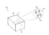
図1に示すように、センサ素子10は、略直方体状に形成されたセンサ本体11と、センサ本体11における対向する側面にそれぞれ固着された一対の電極12とから構成されている。これら電極12は、センサ本体11と電気的に接続されている。
Hereinafter, an embodiment in which the present invention is embodied in a tactile sensor will be described with reference to FIGS. First, the structure of the sensor element will be described.
<Structure of sensor element>
As shown in FIG. 1, the
センサ本体11は、弾力性を有する誘電性の媒体(例えば、シリコーン樹脂)11aと、この媒体11a中に分散された複数のコイル状炭素繊維11bとから構成されている。コイル状炭素繊維11bは、コイル状に形成された非晶質の炭素繊維であり、本実施形態におけるコイル状炭素繊維11bは、太さ(繊維径)が1nm〜10μm、直径(コイル径)が1nm〜50μm、長さ(コイル長さ)が10nm〜10mmとなるように形成されている。なお、本明細書における繊維径という概念には、断面円形状に形成された炭素繊維の直径に限らず、断面楕円形状に形成された炭素繊維の長辺の長さや、断面四角状に形成された炭素繊維の長辺の長さ等も含むものとする。
The
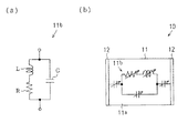
コイル状炭素繊維11bは、コイル状に形成された導電性の繊維であるため、図2(a)に示すように、インダクタンス成分(L成分)、容量成分(C成分)、及び抵抗成分(R成分)をそれぞれ有している。これら成分は、LCR共振回路を構成している。このため、コイル状炭素繊維11bが媒体11a中に分散した状態では、複数のコイル状炭素繊維11bが容量成分(結合容量)により相互に結合された状態となっている。
Since the coiled
<センサ素子による検出の原理>
このように構成されたセンサ素子10に例えば押圧力(外力)が加わった場合、コイル状炭素繊維11bのコイル長さは変化する。コイル状炭素繊維11bのコイル長さ、つまりコイルのピッチが変化することにより、R成分及びリアクタンス成分(L成分及びC成分)は変化する。また、センサ素子10の体積が変化することにより、結合容量も変化する。したがって、電極12を介してR成分やリアクタンス成分を検出することにより、センサ素子10に加わる外力を検出することができる。
<Principle of detection by sensor element>
For example, when a pressing force (external force) is applied to the
以上から、センサ素子10の等価回路は、図2(b)に示すように、可変抵抗器、可変コンデンサ、及び可変インダクタンスにより構成されるLCR共振回路で表される。
<触覚センサの構成>
次に、センサ素子10を備える触覚センサについて説明する。
From the above, the equivalent circuit of the
<Configuration of tactile sensor>
Next, a tactile sensor including the
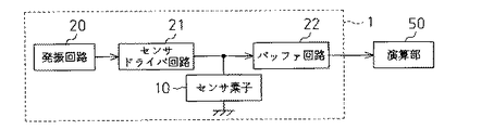
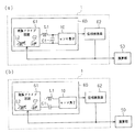
図3に示すように、触覚センサ1は、基準信号入力手段としての発振回路20と、センサ素子10と、検出手段及び信号調整手段としての移相部30と、検出手段としての検波部35とを備えている。検波部35は、第1検波器としての同相検波器36及び第2検波器としての直交検波器37を備えている。発振回路20は、センサドライバ回路21を介してセンサ素子10に接続されている。センサ素子10は、バッファ回路22を介して検波部35に接続されている。また、発振回路20は、移相部30を介して検波部35に接続されている。
As shown in FIG. 3, the
発振回路20は、予め設定された周波数の交流信号(基準信号)をセンサドライバ回路21に出力する。詳しくは、発振回路20は、周波数f0(本実施形態においては200kHz前後)及び振幅Aの正弦波を出力する。なお、発振回路20は、時間の経過に伴って振幅が変化する交流信号を出力する構成であればよく、正弦波を出力する構成に限定されない。例えば、発振回路20は、三角波や方形波等を出力するように構成されてもよい。本実施形態における発振回路20は、予め設定された周波数範囲内の周波数を生成可能なファンクションジェネレータLSIにより構成されている。しかし、この構成に限定されず、発振回路20は、所定の周波数の交流信号を出力する水晶発振回路を用いて構成されてもよい。
The
センサドライバ回路21は、センサ素子10の駆動が可能な振幅レベルに基準信号の振幅を変換して、センサ素子10の一方の電極12に出力する。センサドライバ回路21は、センサ素子10が有するインピーダンスの影響によって基準信号が歪むことを防止するために、入力インピーダンスが高く、出力インピーダンスが低くなるように構成される。本実施形態におけるセンサドライバ回路21は、利得「1」の正相増幅器(いわゆるボルテージフォロワ)により構成されている。
The
バッファ回路22は、センサ素子10の他方の電極12から入力される信号(センサ出力信号)を検波部35に出力する回路である。バッファ回路22は、検波部35の回路構成によってセンサ出力信号が変動しないように、入力インピーダンスが高くなるように構成されている。また、センサ素子10のセンサ出力信号は微小であるため、本実施形態におけるバッファ回路22は、増幅器の機能を有している。具体的には、バッファ回路22は、非反転型増幅器により構成されている。このため、利得の調整により増幅度が調整される。
The
移相部30は、移相器31及び直交用移相器としての90°移相器32を備えている。移相器31は、発振回路20から入力された基準信号の位相を遅らせたり進めたりする回路である。移相器31は、入力された信号の全ての周波数成分を通過させるフィルタ(オールパスフィルタ)により構成されている。移相器31は、この位相が相違させられた基準信号(検波基準信号としての同相信号)を検波部35の同相検波器36に出力するとともに、90°移相器32に出力する。移相器31は、基準信号の位相を調整することにより、センサ素子10に外力が加わっていない状態におけるセンサ出力信号の位相と同相信号の位相とを一致させる。
The
90°移相器32は、同相信号の位相を90°だけ遅らせる回路である。すなわち、90°移相器32は、センサ素子10に外力が加わっていない状態(R成分及びリアクタンス成分が変化しない状態)におけるセンサ出力信号に対して90°の位相差となるように、基準信号を移相させる回路である。90°移相器32は、移相器31と同様の構成を有し、移相器31における位相の調整量が90°に固定された構成となっている。90°移相器32は、入力された同相信号に対して90°遅れた信号を直交信号として直交検波器37に出力する。
The 90 ° phase shifter 32 is a circuit that delays the phase of the in-phase signal by 90 °. That is, the 90 ° phase shifter 32 has a reference signal so as to have a 90 ° phase difference with respect to the sensor output signal when no external force is applied to the sensor element 10 (the R component and the reactance component do not change). Is a circuit for shifting the phase. The 90 ° phase shifter 32 has a configuration similar to that of the
検波部35は、同相検波器36及び直交検波器37により、バッファ回路22を介して入力されたセンサ出力信号を直交検波する。本実施形態においては、検波部35は、直交検波の方式としてプロダクト検波を用いている。すなわち、検波部35は、位相が90°だけ互いに異なり、振幅及び周期が同一の2つの正弦波を用いてセンサ出力信号を検波する。
The
同相検波器36は、同相信号によりセンサ出力信号を検波してオフセットアンプ回路38に出力する。具体的には、同相検波器36は、同相信号とセンサ出力信号とを乗算して出力する。例えば、同相信号として「A・sin(ωt)(ここで、ω=2πf0)」で示される正弦波が入力され、センサ出力信号として「A’sin(ωt+ψ)(ψ:センサ素子10による位相遅れ)」で示される正弦波が入力された場合、同相検波器36は、「A・A’・sin(ωt)・sin(ωt+ψ)」で示される信号を出力する。同相検波器36は、この信号成分のうち同相信号の2倍の周波数の信号成分「cos(2ωt+ψ)」をローパスフィルタにより除去して、「α・cos(ψ)(αは、A及びA’により定まる直流電圧であり、以下「振幅電圧」という)」として示される直流電圧(同相検波電圧I)を出力する。
The in-
一方、直交検波器37は、直交信号によりセンサ出力信号を検波してオフセットアンプ回路39に出力する。具体的には、直交検波器37は、直交信号とセンサ出力信号とを乗算して出力する。例えば、直交信号として「A・cos(ωt)(同相信号に対して90°位相が遅れた信号)」で示される正弦波が入力され、センサ出力信号として「A’sin(ωt+ψ)」で示される正弦波が入力された場合、直交検波器37は、「A・A’・cos(ωt)・sin(ωt+ψ)」で示される信号を出力する。直交検波器37は、この信号成分のうち直交信号の2倍の周波数の信号成分「sin(2ωt+ψ)」をローパスフィルタにより除去して、「α’・sin(ψ)(α’は、A及びA’により定まる定数)」として示される直流電圧(直交検波電圧Q)を出力する。
On the other hand, the
オフセットアンプ回路38は、基準電源40で示される電圧を同相検波電圧Iから減算して検出電圧V1として出力する。同様に、オフセットアンプ回路39は、基準電源40で示される電圧を直交検波電圧Qから減算して検出電圧V2として出力する。なお、本実施形態におけるオフセットアンプ回路38,39は、減算増幅器により構成されている。オフセットアンプ回路38やオフセットアンプ回路39の減算量の調整により、センサ素子10に外力が加わっていないときの検出電圧V1,V2の値は「0」に設定されている。
The offset
演算部50は、入力された検出電圧V1、V2に基づいて、センサ素子10に加わった外力の変化量や種類を求める。以下、触覚センサ1による被検出量の検出原理について、図4及び図5に基づいて具体的に説明する。ここでは、触覚センサ1に対して指によって外力が加えられた場合を例にして説明する。なお、検出電圧V1及び検出電圧V2は、同相検波電圧I及び直交検波電圧Qをそれぞれオフセットさせることにより得られる電圧値であり、これら検波電圧I,Qの挙動に連動して変動する。そこで、以下、同相検波電圧I及び直交検波電圧Qに基づく検出原理について説明する。
The
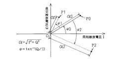
<同相検波電圧I及び直交検波電圧Qに基づく検出原理>
図4に示すように、センサ素子10に外力が加わっていない状態において、同相検波電圧IをX成分、直交検波電圧QをY成分として極座標表示すると(ポイントP0)、原点OからポイントP0までの仮想線のX軸に対する傾きは位相遅れψ0、原点OからポイントP0までの長さは振幅電圧αとなる。なお、本実施形態においては、移相器31により、センサ素子10に外力が加わっていない状態におけるセンサ出力信号の位相と同相信号の位相とは一致しているため、位相遅れψは「0[rad]」(ψ0=0[rad])となる。ここでは、説明の便宜上、ψ0を図面上に表示している。
<Detection principle based on in-phase detection voltage I and quadrature detection voltage Q>
As shown in FIG. 4, in the state where no external force is applied to the
センサ素子10に外力が加わった際、例えば、位相遅れψが増大するとともに振幅電圧αが減少して同相検波電圧I及び直交検波電圧QがポイントP1で示される場合、センサ素子10のR成分及びL成分が増加し、C成分が減少したと推定される。詳しくは、振幅電圧αが振幅電圧α0から振幅電圧α1に減少していることから、センサ出力信号の振幅が減少したと推定され、R成分が増加したと推定される。また、位相遅れψが位相遅れψ0から位相遅れψ1に増加していることから、同相信号に対するセンサ出力信号の位相遅れψが増加したと推定され、L成分が増加するとともにC成分が減少したと推定される。
When an external force is applied to the
一方、センサ素子10に外力が加わった際、例えば、位相遅れψが減少するとともに振幅電圧αが増大して同相検波電圧I及び直交検波電圧QがポイントP2で示される場合、センサ素子10のC成分が増加し、R成分及びL成分が減少したと推定される。詳しくは、振幅電圧αが振幅電圧α0から振幅電圧α2に増大していることから、センサ出力信号の振幅が増大したと推定され、R成分が減少したと推定される。また、位相遅れψが位相遅れψ0から位相遅れψ1に減少していることから、同相信号に対するセンサ出力信号の位相遅れψが減少したと推定され、C成分が増加するとともにL成分が減少したと推定される。
On the other hand, when an external force is applied to the
このように、演算部50は、センサ素子10に外力が加わっていない状態からの振幅電圧α及び位相遅れψの変化傾向や変化量を算出することによって、センサ素子10に外力が加わることにより変化する成分(R成分、リアクタンス成分)を検出することができる。振幅電圧α及び位相遅れψは、センサ素子10に加わる外力の種類(指で押したのか、針で突いたのか等)やその大きさにより変動する。よって、振幅電圧α及び位相遅れψの変化パターンによってセンサ素子10に加わる外力の種類や大きさを検出することができる。
As described above, the
<触覚センサ1による外力の微小な変化の検出>
センサ素子10は、非常に小さなコイル状炭素繊維11bが弾力性を有する媒体11a中に分散されることにより構成されている。このため、センサ素子10に外力が加わると、その外力の微小な変化により、媒体11aの体積が変化するとともに、コイル状炭素繊維11bは圧縮または伸張する。このようにコイル状炭素繊維11bの形状が変化することにより、コイル状炭素繊維11bが有するR成分及びリアクタンス成分は変化する。また、媒体11aの体積変化によりC成分が変化する。したがって、センサ素子10に加わる外力の微小な変化により、センサ素子10のR成分及びリアクタンス成分が変化する。
<Detection of minute changes in external force by the
The
これらR成分の変化及びリアクタンス成分の変化により、センサ出力信号が変化する。センサ出力信号の変化は、検波部35における直交検波により検出される。そして、前述したように、R成分及びリアクタンス成分の変化傾向や変化量が求められる。したがって、触覚センサ1により、センサ素子10に加わる外力の微小な変化を検出することができる。
The sensor output signal changes due to the change in the R component and the change in the reactance component. The change in the sensor output signal is detected by quadrature detection in the
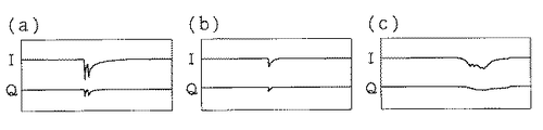
図5には、センサ素子10に対して指で外力を加えた場合における同相検波電圧Iと直交検波電圧Qとの測定結果を示す。図5(a)は、センサ素子10の表面を指で押圧した場合を、図5(b)は、センサ素子10の表面を指で軽く触れた場合を、図5(c)は、センサ素子10の表面を指で撫でた場合をそれぞれ示す。各図に示すように、同相検波電圧I及び直交検波電圧Qは、センサ素子10に加えられる外力の種類及び大きさにより影響を受けることが確かめられた。
FIG. 5 shows measurement results of the in-phase detection voltage I and the quadrature detection voltage Q when an external force is applied to the
したがって上記実施形態によれば、以下のような効果を得ることができる。
(1)センサ素子10を構成するコイル状炭素繊維11bは、繊維径が1nm〜10μm、コイル径が1nm〜50μm、コイル長さが10nm〜10mmとなるように形成されている。このため、センサ素子10は、センサ素子10に加わる外力の微小な変化にも応答して、そのR成分及びリアクタンス成分を変化させる。検波部35は、これらR成分やリアクタンス成分に基づいて変化するセンサ出力信号を検波する。したがって、触覚センサ1に加わる外力の微小な変化を検出することができる。
Therefore, according to the above embodiment, the following effects can be obtained.
(1) The coiled
(2)発振回路20は、正弦波からなる基準信号を出力する。検波部35は、この時間の経過とともに振幅が変化する基準信号を用いてセンサ出力信号を直交検波する。このため、こうした触覚センサ1によれば、センサ素子10のR成分の変化及びリアクタンス成分の変化の両方を検出することができる。よって、演算部50は、これら両成分の変化により、センサ素子10に加わった外力を総合的に検出することができる。つまり、こうした触覚センサ1では、R成分とリアクタンス成分とを共に変化させる外力が加わった場合は勿論、R成分のみを変化させる外力やリアクタンス成分のみを変化させる外力をも検出することができ、該外力の大きさや種類を演算部50による演算処理によって求めることが可能となる。したがって、該触覚センサ1によれば、被検出量の微小な変化を確実に検出することができる。すなわち、高感度の触覚センサ1とすることができる。
(2) The
また、演算部50は、振幅電圧α及び位相遅れψを共に算出することができるため、R成分の変化量(=A’−A)とリアクタンス成分の変化量(位相遅れψ)とを高精度に求めることができる。よって、例えば演算部50が振幅電圧αのみを算出し、位相遅れψを算出しない場合、すなわちR成分の変化量のみを算出する場合においても、該R成分の変化量を高精度に求めることができる。つまり、この場合においても、演算部50は、R成分の変化量に基づく外力の大きさや種類を求めることができることとなる。同様に、例えば演算部50が位相遅れψのみを算出し、振幅電圧αを算出しない場合、すなわち、リアクタンス成分の変化量のみを算出する場合においても、該リアクタンス成分の変化量を高精度に求めることができる。つまり、この場合においても、演算部50は、リアクタンス成分の変化量に基づく外力の大きさや種類を求めることができることとなる。
Further, since the
(3)移相器31により、センサ素子10に外力が加わっていない状態においては基準信号の位相とセンサ出力信号の位相とは同相となる。このため、検波部35は、センサドライバ回路21やバッファ回路22による位相遅れψ、または外力が加わっていない状態におけるセンサ素子10自身による位相遅れψを排除してセンサ出力信号を検波することができる。したがって、触覚センサ1の回路構成上生じる位相遅れψを考慮することなく、センサ素子10に加わる外力を検出することができる。
(3) Due to the
(4)センサ出力信号にノイズ(電気信号の乱れ)が重畳してしまうと、その振幅は変化する。演算部50は、同相検波電圧I(検出電圧V1)、直交検波電圧Q(検出電圧V2)によりセンサ出力信号と基準信号との移相遅れψを求めるため、ノイズの影響を抑制しつつ被検出量の微小な変化を精度よく検出することができる。
(4) If noise (electric signal disturbance) is superimposed on the sensor output signal, its amplitude changes. The
(5)触覚センサ1は、バッファ回路22及び移相器31を備えている。これら回路は、製造ばらつきによるセンサ素子10のR成分やリアクタンス成分のばらつきを吸収することができる。つまり、センサ素子10のR成分のばらつきは主としてバッファ回路22により、リアクタンス成分のばらつきは主として移相器31により吸収できる。したがって、触覚センサ1の特性を揃えるための製造設備を構築する必要がなく、触覚センサ1の製造コストを抑制することができる。
(5) The
なお、本発明の実施形態は以下のように変更してもよい。
・前記実施形態において、移相器31には、発振回路20から基準信号が入力されている。しかし、移相器31には、発振回路20に代わってセンサドライバ回路21から基準信号に相当する信号が入力されてもよい。この場合、発振回路20及びセンサドライバ回路21が基準信号入力手段に相当する。このようにしても、基準信号に基づいてセンサ出力信号を検波することができる。
In addition, you may change embodiment of this invention as follows.
In the above embodiment, the reference signal is input from the
・前記実施形態において、触覚センサ1は、オフセットアンプ回路38,39を備えなくてもよい。このように構成しても、前記(1)〜(5)に示す効果と同様の効果を得ることができる。この場合、演算部50は、同相検波電圧I及び直交検波電圧Qに基づいてセンサ素子10に加えられる外力を求めるように変更される。なお、演算部50により求められる振幅電圧α及び移相遅れψは、基準信号に対する相対的な変化量となる。
In the embodiment, the
・前記実施形態において、触覚センサ1は、90°移相器32、直交検波器37、及びオフセットアンプ回路39を備えていなくてもよい。
この場合、演算部50には前記同相検波電圧I(=α・cos(ψ))のみが入力されることとなるものの、該演算部50は、該同相検波電圧Iにおける振幅電圧αの変化量を近似的に求めることが可能となる。つまり、演算部50は、リアクタンス成分の変化量については算出できないものの、R成分の変化量を近似的に算出することが可能となる。よって、こうした変更態様においても、演算部50は、R成分の変化量に基づき、触覚センサ1に加わる外力の微小な変化を検出することが可能となる。しかも、このようにすれば、触覚センサ1の構成を簡単にすることができる。
In the embodiment, the
In this case, although only the in-phase detection voltage I (= α · cos (ψ)) is input to the
また、例えば、同相検波器36は、前記同相検波電圧Iを出力せず、同相信号に対するセンサ出力信号の振幅変化及び位相遅れψのうちの少なくとも一方を示す検波信号を出力するように変更されてもよい。このようにしても、演算部50は、センサ素子10におけるR成分の変化及びリアクタンス成分の変化の少なくとも一方を検出することができるため、触覚センサ1に加わる外力の微小な変化を検出することができる。
Further, for example, the in-
・センサ素子10に加わった外力を検出する方法は、前記実施形形態における直交検波方式を用いた方法に限定されない。例えば、図6に示すように、センサドライバ回路21は、センサ素子10を介して接地されるとともにバッファ回路22に接続されてもよい。この場合、演算部50は、センサ素子10の端子間電圧に基づいてセンサ素子10に加わる外力を求めるように変更される。すなわち、センサ素子10の端子間電圧(出力電圧)を直接検出する「出力電圧の直接検出方式」により、センサ素子10に加わった外力を検出するようにしてもよい。このようにすれば、触覚センサ1の回路構成を簡単にすることができる。なお、このような構成におけるセンサ素子10は、検出手段としても機能する。
The method for detecting the external force applied to the
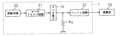
・また、触覚センサ1は、図7に示すように、センサ素子10がシャント抵抗Rs(検出手段)を介して接地されるともに、バッファ回路22に接続されることにより構成されてもよい。センサ素子10からの出力電流は、シャント抵抗Rsにより電圧に変換される。演算部50は、シャント抵抗Rsの端子間電圧に基づいてセンサ素子10に加わる外力を求めるように変更される。すなわち、センサ素子10に流れる電流をシャント抵抗Rsにより検出する「出力電流の直接検出方式」により、センサ素子10に加わった外力を検出するようにしてもよい。このような構成にしても、触覚センサ1の回路構成を簡単にすることができる。
As shown in FIG. 7, the
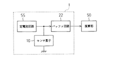
・また、触覚センサ1は、図8に示すように、センサ素子10の一方の電極12が接地されるとともに、他方の電極12が定電流回路55に接続されることにより構成されてもよい。ここで、定電流回路55は、センサ素子10に対して直流電流を流す回路である。演算部50は、センサ素子10の端子間電圧に基づいてセンサ素子10に加わる外力を求めるように変更される。このように構成すれば、センサ素子10におけるR成分やリアクタンス成分の変化により、センサ素子10の端子間抵抗が変化する。この端子間抵抗の変化は、センサ素子10の端子間電圧の変化として現れる。したがって、演算部50は、センサ素子10の端子間電圧により、センサ素子10におけるR成分やリアクタンス成分の変化を求めることができる。すなわち、センサ素子10に一定電流を流した状態で、センサ素子10の端子間抵抗の変化を検出する「抵抗値変化検出方式」により、センサ素子10に加わった外力を検出するようにしてもよい。
As shown in FIG. 8, the
・更に、触覚センサ1は、図9に示すように、センサ素子10を用いて発振部60を構成し、該発振部60から出力される発振信号の周波数の変化からセンサ素子10に加わる外力を検出するように構成されてもよい。詳しくは、触覚センサ1は、発振ドライブ回路61(基準信号入力手段)とセンサ素子10とにより構成される発振部60を備えてもよい。この発振部60は、センサ素子10のR成分及びリアクタンス成分の変化により周波数や振幅が変動する発振信号を出力するように構成される。
Furthermore, as shown in FIG. 9, the
具体的には、発振部60は、センサ素子10のリアクタンス成分が容量性の場合には、図9(a)に示すように、センサ素子10とコンデンサC1とが並列となるように構成される。一方、発振部60は、センサ素子10のリアクタンス成分が誘導性の場合には、図9(b)に示すように、センサ素子10とコイルL1とが直列となるように構成される。発振ドライブ回路61は、リアクタンス調整手段としての可変コイルL2及び可変コンデンサC2を備えている。発振ドライブ回路61は、後述する制御信号に基づいて可変コイルL2または可変コンデンサC2の値を調整可能に構成されている。このような構成により、発振部60は、コイルL1、可変コイルL2、コンデンサC1、及び可変コンデンサC2のそれぞれの値で定まる周波数を有する発振信号を出力する。位相検波器62(検出手段)は、予め設定された基準発振周波数に対して発振信号の周波数が大きくなったり小さくなったりした場合、その周波数の変化量に基づいて周波数の変動を抑制するべく制御信号を発振ドライブ回路61に出力する。つまり、位相検波器62は、発振信号の周波数が大きくなった場合には発振信号の周波数を小さくする旨の制御信号を、発振信号の周波数が小さくなった場合には発振信号の周波数を大きくする旨の制御信号を出力する。また、位相検波器62は、制御信号を、センサ素子10におけるリアクタンス成分の変化量として演算部50に出力する。演算部50は、制御信号に基づいてセンサ素子10に加わる外力を求める。
Specifically, when the reactance component of the
このような構成によれば、センサ素子10のリアクタンス成分の変化分は、発振信号の周波数の変化分を介して間接的に検出される。このため、触覚センサ1の被検出量の変化が微小なためにセンサ素子10のリアクタンス成分の変化が微弱となっても、センサ素子10に加わる外力を発振信号の周波数の変化として確実に検出することができる。また、位相検波器62に加えて、発振信号の振幅を検出する回路を備えれば、演算部50は、その振幅の変化に基づいて、センサ素子10におけるR成分の変化をも求めることができる。
According to such a configuration, the change in the reactance component of the
・前記実施形態における触覚センサ1は、移相器31により、センサ素子10に外力が加わっていない状態におけるセンサ出力信号の位相と同相信号の位相とを一致させている。しかし、触覚センサ1は、移相器31によらないで、両信号の位相を一致させるように構成されてもよい。例えば、電気的な特性が同一のセンサ素子10を別途用意し、このセンサ素子10を移相器31の代わりに用いてもよい。このようにしても、同相信号の位相とセンサ出力信号の位相とを一致させることができる。また、このように、同一のセンサ素子10を2つ使用した場合、位相のみならず、センサ素子10に外力が加わっていない状態におけるセンサ出力信号の振幅と同相信号の振幅とをも一致させることができる。したがって、製造ばらつきによるセンサ素子10のR成分及びリアクタンス成分のばらつきを吸収することができる。
In the
・前記実施形態において90°移相器は、同相信号の位相を90°だけ遅らせることにより直交用移相器として用いられている。しかし、90°移相器32は、移相器31における基準信号の移相量に90°加算した分だけ基準信号を移相させることにより直交用移相器として用いられてもよい。要するに、直交用移相器は、センサ素子10に外力が加わっていない状態におけるセンサ出力信号に対して90°の位相差となるように、基準信号を移相させる構成であればよい。
In the embodiment, the 90 ° phase shifter is used as a quadrature phase shifter by delaying the phase of the in-phase signal by 90 °. However, the 90 ° phase shifter 32 may be used as an orthogonal phase shifter by shifting the phase of the reference signal by an amount obtained by adding 90 ° to the phase shift amount of the reference signal in the
・前記実施形態において発振回路20は、交流信号に代わって直流信号を出力するように変更されてもよい。この場合、演算部50は、バッファ回路22からの出力に基づいてセンサ素子10に加わった外力を検出するように変更される。演算部50は、直流信号の電圧値の変化からセンサ素子10のR成分の変化を検出する。このような構成によると、触覚センサ1の回路構成を簡単にすることができる。特に、センサ素子10のR成分を大きく変化させる外力がセンサ素子10に加わった場合には、このような回路構成による検出が特に有効となる。
In the embodiment, the
・センサ素子10は、コイル状炭素繊維11bのみ、コイル状炭素繊維11bを含んだものに限定されない。例えば、センサ素子10は、銅や銀等の金属材料、炭化チタン(TiC)、窒化チタン(TiN)、酸化亜鉛(ZnO)等の合金材料、炭素材料、ポリアセチレン等の高分子材料などの導電性繊維が、線状、コイル状、または筒状等に形成されたものが媒体11a中に分散された構成となっていてもよい。この導電性繊維の製造方法は特に限定されず、例えば気相成長法等が挙げられる。導電性繊維の具体例としては、前記コイル状炭素繊維11bの他に、カーボンナノチューブ、VGCF(気相成長炭素繊維)、PAN系炭素繊維やピッチ系炭素繊維等の炭素繊維、導電性ウィスカ等が挙げられる。これらは単独でセンサ素子10を構成してもよいし、二種以上が組み合わされてセンサ素子10を構成してもよい。これら導電性繊維は、太さがμm単位以下の寸法に形成されているため、コイル状炭素繊維11bと同様に、被検出量の微小な変化にも反応してそのR成分やリアクタンス成分が変化する。つまり、センサ素子に外力が加わって導電性繊維が曲がると、導電性繊維内に歪が発生してR成分が変化するとともに、曲がる前に比較して媒体11aと導電性繊維との位置関係が相違することによりリアクタンス成分が変化する。これら導電性繊維を用いたセンサ素子を用いた触覚センサによっても、前記(1)〜(5)に示す効果と同様の効果を得ることができる。
The
また、センサ素子10は、これら導電性繊維とコイル状炭素繊維11bとの混合物が媒体11a中に分散された構成となっていてもよい。例えば、VGCFとコイル状炭素繊維11bとの混合物が媒体11a中に分散されたセンサ素子10を適用した場合には、センサ出力信号が安定して被検出量の微小変化を精度よく検出することができることが、本願の発明者により実験で確認されている。また、センサ素子10は、媒体11a中に圧電体粉末が分散されることにより構成されてもよい。圧電体粉末の具体例としてはフェライト、酸化チタン(TiO2)、ジルコン酸鉛(PbZrO3)、チタン酸鉛(PbTiO3)、ジルコン酸チタン酸鉛(PbZrTiO3)、チタン酸バリウム(BaTiO3)等が挙げられる。このように構成しても、センサ素子10からのセンサ出力信号が安定して被検出量の微小変化を精度よく検出することができる。
The
・コイル状炭素繊維11bは、必ずしも非晶質である必要はなく、コイル状に形成された結晶質の炭素繊維によって構成されていてもよい。
・本発明によるセンサは、触覚センサ1以外の用途にも適用することができる。例えば、本発明のセンサは、歪センサ、微振動センサ、味覚センサ、光センサ、電磁波センサ、超音波センサ、温度センサ、湿度センサ、流量センサ、加速度センサ、角速度センサ等にも適用することができる。要するに、センサ素子10のR成分、L成分、及びC成分のいずれかを変動させる被検出量であれば、本センサにより検出することが可能である。
-
The sensor according to the present invention can be applied to uses other than the
次に、前記実施形態から把握できる技術的思想を以下に追記する。
(1)請求項1に記載のセンサにおいて、前記検出手段は、前記センサ素子の端子間における電圧を前記センサ出力信号として検出すること。
Next, the technical idea that can be grasped from the embodiment will be added below.
(1) In the sensor according to
(2)請求項1に記載のセンサにおいて、前記センサ素子に直列に接続される抵抗素子を備え、前記検出手段は、前記抵抗素子の端子間電圧を前記センサ出力信号として検出すること。
(2) The sensor according to
(3)請求項1に記載のセンサにおいて、前記基準信号入力手段は、前記センサ素子に一定電流を流す定電流回路であり、前記検出手段は、前記センサ素子の端子間における抵抗値の変化を検出すること。
(3) In the sensor according to
1…センサとしての触覚センサ、10…センサ素子、11a…媒体、20…基準信号入力手段としての発振回路、30…信号調整手段としての移相部、31…検出手段としての移相器、32…検出手段及び直交用移相器としての90°移相器、35…検出手段としての検波部、36…検出手段及び第1検波器としての同相検波器、37…検出手段及び第2検波器としての直交検波器、55…基準信号入力手段としての電流回路、60…発振部、62…位相検波器、Rs…検出手段としてのシャント抵抗、C2…リアクタンス調整手段としての可変コンデンサ、L2…リアクタンス調整手段としての可変コイル。
DESCRIPTION OF
Claims (10)
前記センサ素子に基準信号を出力する基準信号入力手段と、
前記基準信号の入力に対する前記センサ素子の抵抗成分及びリアクタンス成分のうち少なくとも一方の変化に基づくセンサ出力信号を検出する検出手段とを備えるセンサ。 A sensor element configured by dispersing carbon fibers having a coil shape with a thickness of μm or less in a dielectric medium;
A reference signal input means for outputting a reference signal to the sensor element;
And a sensor that detects a sensor output signal based on a change in at least one of a resistance component and a reactance component of the sensor element with respect to an input of the reference signal.
前記検出手段は、前記基準信号に基づく検波基準信号を用いて前記センサ出力信号を検波する請求項1に記載のセンサ。 The reference signal is an AC signal whose amplitude changes over time,
The sensor according to claim 1, wherein the detection unit detects the sensor output signal using a detection reference signal based on the reference signal.
前記検出手段は、前記検波基準信号を用いて前記センサ出力信号を検波する第1検波器と、前記直交信号を用いて前記センサ出力信号を検波する第2検波器とを備える請求項3または請求項4に記載のセンサ。 The signal adjustment means generates a quadrature signal by shifting the detection reference signal so that a phase difference of 90 ° is obtained with respect to the sensor output signal in a state where the resistance component and reactance component of the sensor element are not changed. With a quadrature phase shifter
The said detection means is provided with the 1st detector which detects the said sensor output signal using the said detection reference signal, and the 2nd detector which detects the said sensor output signal using the said orthogonal signal. Item 5. The sensor according to item 4.
前記検出手段は、前記発振信号の周波数及び振幅のうち少なくとも一方を検出する請求項1に記載のセンサ。 The reference signal input means and the sensor element constitute an oscillation unit that outputs an oscillation signal whose frequency varies due to a change in reactance component of the sensor element and whose amplitude varies due to a change in the resistance component of the sensor element,
The sensor according to claim 1, wherein the detection unit detects at least one of a frequency and an amplitude of the oscillation signal.
前記検出手段は、前記発振信号の周波数の変化量を検出する位相検波器を備え、該変化量を前記センサ素子におけるリアクタンス成分の変化として検出するとともに、該変化量に基づいて該周波数の変化を抑制するべく前記制御信号を出力する請求項7に記載のセンサ。 The reference signal input means includes reactance adjustment means for changing the frequency of the oscillation signal, and when a control signal for changing the frequency of the oscillation signal is input, the frequency of the oscillation signal by the reactance adjustment means Adjust
The detection means includes a phase detector that detects a change in frequency of the oscillation signal, detects the change as a change in reactance component in the sensor element, and detects a change in the frequency based on the change. The sensor according to claim 7, wherein the control signal is output for suppression.
前記センサ素子に基準信号を出力する基準信号入力手段と、
前記基準信号の入力に対する前記センサ素子の抵抗成分及びリアクタンス成分のうち少なくとも一方の変化に基づくセンサ出力信号を検出する検出手段とを備えるセンサ。 A sensor element formed by dispersing elastic conductive fibers having a thickness of μm or less in a dielectric medium;
A reference signal input means for outputting a reference signal to the sensor element;
And a sensor that detects a sensor output signal based on a change in at least one of a resistance component and a reactance component of the sensor element with respect to an input of the reference signal.
前記センサ素子に交流信号を出力する基準信号入力手段と、
前記センサ素子の抵抗成分及びリアクタンス成分が変化しない状態において、前記交流信号の入力に対する前記センサ素子の抵抗成分及びリアクタンス成分のうち少なくとも一方の変化に基づくセンサ出力信号に対して90°の位相差となるように前記交流信号を移相させて、直交信号を生成する直交用移相器を備え、
前記交流信号に基づく検波基準信号を用いて前記センサ出力信号を検波する第1検波器と、
前記直交信号を用いて前記センサ出力信号を検波する第2検波器とを備えるセンサ。 A sensor element having a resistance component and a reactance component, wherein at least one of the resistance component and the reactance component changes based on a change in the detected amount;
Reference signal input means for outputting an AC signal to the sensor element;
A phase difference of 90 ° with respect to a sensor output signal based on a change in at least one of the resistance component and reactance component of the sensor element with respect to the input of the AC signal in a state where the resistance component and reactance component of the sensor element do not change. A phase shifter for quadrature for generating a quadrature signal by shifting the phase of the alternating current signal,
A first detector for detecting the sensor output signal using a detection reference signal based on the AC signal;
A sensor comprising: a second detector that detects the sensor output signal using the orthogonal signal.
Priority Applications (1)
| Application Number | Priority Date | Filing Date | Title |
|---|---|---|---|
| JP2004107606A JP2005291927A (en) | 2004-03-31 | 2004-03-31 | Sensor |
Applications Claiming Priority (1)
| Application Number | Priority Date | Filing Date | Title |
|---|---|---|---|
| JP2004107606A JP2005291927A (en) | 2004-03-31 | 2004-03-31 | Sensor |
Publications (1)
| Publication Number | Publication Date |
|---|---|
| JP2005291927A true JP2005291927A (en) | 2005-10-20 |
Family
ID=35325014
Family Applications (1)
| Application Number | Title | Priority Date | Filing Date |
|---|---|---|---|
| JP2004107606A Pending JP2005291927A (en) | 2004-03-31 | 2004-03-31 | Sensor |
Country Status (1)
| Country | Link |
|---|---|
| JP (1) | JP2005291927A (en) |
Cited By (7)
| Publication number | Priority date | Publication date | Assignee | Title |
|---|---|---|---|---|
| WO2007086358A1 (en) * | 2006-01-24 | 2007-08-02 | Shimadzu Corporation | Proximity and contact sensor and sensor element |
| JP2007201641A (en) * | 2006-01-24 | 2007-08-09 | Gifu Univ | Proximity sensor and proximity / contact sensor |
| JP2008082711A (en) * | 2006-09-25 | 2008-04-10 | Gifu Univ | Sensor element, object detection sensor, and object detection method using object detection sensor |
| JP2010271087A (en) * | 2009-05-19 | 2010-12-02 | Nippon Telegr & Teleph Corp <Ntt> | measuring device |
| US7868628B2 (en) | 2007-08-16 | 2011-01-11 | Tdk Corporation | Tactile sensor utilizing microcoils with spiral shape |
| JP2013115682A (en) * | 2011-11-30 | 2013-06-10 | Pentel Corp | Capacitive coupling type electrostatic sensor |
| JP2013135346A (en) * | 2011-12-27 | 2013-07-08 | Pentel Corp | Capacitance coupling type electrostatic sensor |
Citations (11)
| Publication number | Priority date | Publication date | Assignee | Title |
|---|---|---|---|---|
| JPS62127628A (en) * | 1985-11-29 | 1987-06-09 | Anritsu Corp | Saw force sensor |
| JPS634601A (en) * | 1986-06-25 | 1988-01-09 | 横浜ゴム株式会社 | Ac driving method of pressure-sensitive conductive rubber |
| JPH02293620A (en) * | 1989-05-08 | 1990-12-04 | Murata Mfg Co Ltd | Vibration gyro |
| JPH07248270A (en) * | 1994-03-09 | 1995-09-26 | Omron Corp | Signal processing device and cutting tool condition detection device |
| JPH10256003A (en) * | 1997-03-07 | 1998-09-25 | Thueringisches Inst Fuer Textil & Kunststoff Forsch Ev | Manufacture of sensor material |
| JP2000027072A (en) * | 1998-07-10 | 2000-01-25 | Seiji Motojima | Coiled carbon fiber, method for producing the same, and electromagnetic wave shielding material |
| JP2001146645A (en) * | 1999-11-19 | 2001-05-29 | Seiji Motojima | Coiled carbon fiber composite having ferromagnetism, method for producing the same and electric wave absorber |
| JP2001336995A (en) * | 2000-05-30 | 2001-12-07 | Mitsubishi Electric Corp | Torque detector |
| JP2002134325A (en) * | 2000-07-08 | 2002-05-10 | Lg Electronics Inc | Inductor utilizing carbon nanotube and/or carbon nanofiber |
| JP2002236059A (en) * | 2001-02-08 | 2002-08-23 | Univ Tokyo | Tactile sensor, tactile sensor unit, method of using tactile sensor, method of using tactile sensor unit, and method of manufacturing tactile sensor unit |
| JP2004045277A (en) * | 2002-07-12 | 2004-02-12 | Suzuki Co Ltd | Load detecting method for actuator |
-
2004
- 2004-03-31 JP JP2004107606A patent/JP2005291927A/en active Pending
Patent Citations (11)
| Publication number | Priority date | Publication date | Assignee | Title |
|---|---|---|---|---|
| JPS62127628A (en) * | 1985-11-29 | 1987-06-09 | Anritsu Corp | Saw force sensor |
| JPS634601A (en) * | 1986-06-25 | 1988-01-09 | 横浜ゴム株式会社 | Ac driving method of pressure-sensitive conductive rubber |
| JPH02293620A (en) * | 1989-05-08 | 1990-12-04 | Murata Mfg Co Ltd | Vibration gyro |
| JPH07248270A (en) * | 1994-03-09 | 1995-09-26 | Omron Corp | Signal processing device and cutting tool condition detection device |
| JPH10256003A (en) * | 1997-03-07 | 1998-09-25 | Thueringisches Inst Fuer Textil & Kunststoff Forsch Ev | Manufacture of sensor material |
| JP2000027072A (en) * | 1998-07-10 | 2000-01-25 | Seiji Motojima | Coiled carbon fiber, method for producing the same, and electromagnetic wave shielding material |
| JP2001146645A (en) * | 1999-11-19 | 2001-05-29 | Seiji Motojima | Coiled carbon fiber composite having ferromagnetism, method for producing the same and electric wave absorber |
| JP2001336995A (en) * | 2000-05-30 | 2001-12-07 | Mitsubishi Electric Corp | Torque detector |
| JP2002134325A (en) * | 2000-07-08 | 2002-05-10 | Lg Electronics Inc | Inductor utilizing carbon nanotube and/or carbon nanofiber |
| JP2002236059A (en) * | 2001-02-08 | 2002-08-23 | Univ Tokyo | Tactile sensor, tactile sensor unit, method of using tactile sensor, method of using tactile sensor unit, and method of manufacturing tactile sensor unit |
| JP2004045277A (en) * | 2002-07-12 | 2004-02-12 | Suzuki Co Ltd | Load detecting method for actuator |
Cited By (9)
| Publication number | Priority date | Publication date | Assignee | Title |
|---|---|---|---|---|
| WO2007086358A1 (en) * | 2006-01-24 | 2007-08-02 | Shimadzu Corporation | Proximity and contact sensor and sensor element |
| JP2007201641A (en) * | 2006-01-24 | 2007-08-09 | Gifu Univ | Proximity sensor and proximity / contact sensor |
| US8203349B2 (en) | 2006-01-24 | 2012-06-19 | Shimadzu Corporation | Proximity and contact sensor and sensor element |
| JP2008082711A (en) * | 2006-09-25 | 2008-04-10 | Gifu Univ | Sensor element, object detection sensor, and object detection method using object detection sensor |
| US7868628B2 (en) | 2007-08-16 | 2011-01-11 | Tdk Corporation | Tactile sensor utilizing microcoils with spiral shape |
| US8072227B2 (en) | 2007-08-16 | 2011-12-06 | Tdk Corporation | Method for manufacturing tactile-sensitive material utilizing microcoils |
| JP2010271087A (en) * | 2009-05-19 | 2010-12-02 | Nippon Telegr & Teleph Corp <Ntt> | measuring device |
| JP2013115682A (en) * | 2011-11-30 | 2013-06-10 | Pentel Corp | Capacitive coupling type electrostatic sensor |
| JP2013135346A (en) * | 2011-12-27 | 2013-07-08 | Pentel Corp | Capacitance coupling type electrostatic sensor |
Similar Documents
| Publication | Publication Date | Title |
|---|---|---|
| US8823394B2 (en) | Apparatus for capacitively measuring changes | |
| JP5284911B2 (en) | Capacitance type physical quantity sensor and angular velocity sensor | |
| JP6343984B2 (en) | Non-contact voltage measuring device | |
| CN101918804B (en) | Piezoelectric vibration type force sensor | |
| US20140152327A1 (en) | Capacitive Proximity Sensor As Well As Method For Capacitive Approximation Detection | |
| US9791522B2 (en) | Magnetic field detection sensor | |
| CN110461214A (en) | Measuring properties in the body | |
| CN103787266B (en) | Mechanical part, mechanical system and the method being used for running mechanical part | |
| JP2005291927A (en) | Sensor | |
| JP5711368B2 (en) | Magnetic field detection method and magnetic field detection circuit | |
| JP2017503178A (en) | Pressure transducer with capacitively coupled source electrode | |
| JP4406567B2 (en) | Circuit device for rectifying the output voltage of a sensor fed by an oscillator | |
| US7343802B2 (en) | Dynamic-quantity sensor | |
| US7997135B2 (en) | Angular velocity sensor | |
| US11940503B2 (en) | Magnetic sensor circuit and magnetic field detection device | |
| JP6981711B2 (en) | Non-contact type voltage detector | |
| Wen et al. | Frequency adaptive driver for ultrasonic vibrators with motional current feedback | |
| JP2021025820A (en) | Magnetic field detection sensor | |
| JP6801414B2 (en) | Moisture detector | |
| JP6273443B2 (en) | Physical quantity measurement method using physical quantity measurement circuit | |
| JP2017009414A (en) | Piezoelectric sensor | |
| CN117129021A (en) | A PVDF piezoelectric sensor device that can achieve pressing and holding | |
| JP2017083331A (en) | Capacitance detection device and sensor system | |
| JP2013044527A (en) | Physical quantity detecting sensor, and electronic apparatus | |
| Wena et al. | Frequency Adaptive Driver for Ultrasonic Vibrators with Motional Current Feedback1 |
Legal Events
| Date | Code | Title | Description |
|---|---|---|---|
| A521 | Written amendment |
Free format text: JAPANESE INTERMEDIATE CODE: A523 Effective date: 20060613 |
|
| A621 | Written request for application examination |
Effective date: 20070326 Free format text: JAPANESE INTERMEDIATE CODE: A621 |
|
| A521 | Written amendment |
Effective date: 20070326 Free format text: JAPANESE INTERMEDIATE CODE: A821 |
|
| A977 | Report on retrieval |
Free format text: JAPANESE INTERMEDIATE CODE: A971007 Effective date: 20090917 |
|
| A131 | Notification of reasons for refusal |
Free format text: JAPANESE INTERMEDIATE CODE: A131 Effective date: 20091201 |
|
| A521 | Written amendment |
Free format text: JAPANESE INTERMEDIATE CODE: A523 Effective date: 20100201 |
|
| A131 | Notification of reasons for refusal |
Effective date: 20100302 Free format text: JAPANESE INTERMEDIATE CODE: A131 |
|
| A521 | Written amendment |
Free format text: JAPANESE INTERMEDIATE CODE: A523 Effective date: 20100430 |
|
| A02 | Decision of refusal |
Effective date: 20100615 Free format text: JAPANESE INTERMEDIATE CODE: A02 |