JP2005291833A - Defect inspecting device of sample - Google Patents
Defect inspecting device of sample Download PDFInfo
- Publication number
- JP2005291833A JP2005291833A JP2004105371A JP2004105371A JP2005291833A JP 2005291833 A JP2005291833 A JP 2005291833A JP 2004105371 A JP2004105371 A JP 2004105371A JP 2004105371 A JP2004105371 A JP 2004105371A JP 2005291833 A JP2005291833 A JP 2005291833A
- Authority
- JP
- Japan
- Prior art keywords
- inspection
- defect
- sample
- wafer
- defect inspection
- Prior art date
- Legal status (The legal status is an assumption and is not a legal conclusion. Google has not performed a legal analysis and makes no representation as to the accuracy of the status listed.)
- Pending
Links
- 230000007547 defect Effects 0.000 title claims abstract description 186
- 238000007689 inspection Methods 0.000 claims abstract description 294
- 238000001514 detection method Methods 0.000 claims abstract description 56
- 238000010894 electron beam technology Methods 0.000 claims description 40
- 238000003860 storage Methods 0.000 claims description 17
- 230000002457 bidirectional effect Effects 0.000 claims description 7
- 230000001678 irradiating effect Effects 0.000 claims description 7
- 230000002950 deficient Effects 0.000 abstract description 20
- 238000012545 processing Methods 0.000 abstract description 19
- 235000012431 wafers Nutrition 0.000 description 184
- 238000000034 method Methods 0.000 description 61
- 230000003287 optical effect Effects 0.000 description 57
- 239000004065 semiconductor Substances 0.000 description 29
- 238000012546 transfer Methods 0.000 description 27
- 230000008569 process Effects 0.000 description 24
- 238000004519 manufacturing process Methods 0.000 description 19
- 230000006870 function Effects 0.000 description 15
- 239000007789 gas Substances 0.000 description 10
- 230000000737 periodic effect Effects 0.000 description 10
- 230000002093 peripheral effect Effects 0.000 description 10
- 238000010586 diagram Methods 0.000 description 9
- 230000015654 memory Effects 0.000 description 9
- 238000012360 testing method Methods 0.000 description 9
- 230000007246 mechanism Effects 0.000 description 8
- 238000004891 communication Methods 0.000 description 7
- 239000011261 inert gas Substances 0.000 description 6
- 238000013507 mapping Methods 0.000 description 6
- YVWNECBAHBJBSI-HZOWPXDZSA-N (2E,4E)-2,4,6-trimethyldeca-2,4-dienamide Chemical compound CCCCC(C)\C=C(/C)\C=C(/C)C(N)=O YVWNECBAHBJBSI-HZOWPXDZSA-N 0.000 description 5
- 239000002245 particle Substances 0.000 description 5
- 238000005192 partition Methods 0.000 description 5
- 238000006243 chemical reaction Methods 0.000 description 4
- 238000012937 correction Methods 0.000 description 4
- 239000000428 dust Substances 0.000 description 4
- 101000873785 Homo sapiens mRNA-decapping enzyme 1A Proteins 0.000 description 3
- 230000001133 acceleration Effects 0.000 description 3
- 230000005540 biological transmission Effects 0.000 description 3
- 238000004364 calculation method Methods 0.000 description 3
- 238000013461 design Methods 0.000 description 3
- 102100035856 mRNA-decapping enzyme 1A Human genes 0.000 description 3
- 238000011084 recovery Methods 0.000 description 3
- 239000000758 substrate Substances 0.000 description 3
- 230000000007 visual effect Effects 0.000 description 3
- IJGRMHOSHXDMSA-UHFFFAOYSA-N Atomic nitrogen Chemical compound N#N IJGRMHOSHXDMSA-UHFFFAOYSA-N 0.000 description 2
- 238000012935 Averaging Methods 0.000 description 2
- QVGXLLKOCUKJST-UHFFFAOYSA-N atomic oxygen Chemical compound [O] QVGXLLKOCUKJST-UHFFFAOYSA-N 0.000 description 2
- 230000015572 biosynthetic process Effects 0.000 description 2
- 230000005684 electric field Effects 0.000 description 2
- 238000005530 etching Methods 0.000 description 2
- 230000010354 integration Effects 0.000 description 2
- 239000001301 oxygen Substances 0.000 description 2
- 229910052760 oxygen Inorganic materials 0.000 description 2
- 230000035945 sensitivity Effects 0.000 description 2
- MYMOFIZGZYHOMD-UHFFFAOYSA-N Dioxygen Chemical compound O=O MYMOFIZGZYHOMD-UHFFFAOYSA-N 0.000 description 1
- 230000005856 abnormality Effects 0.000 description 1
- 230000008901 benefit Effects 0.000 description 1
- 230000008859 change Effects 0.000 description 1
- 239000003086 colorant Substances 0.000 description 1
- 230000000052 comparative effect Effects 0.000 description 1
- 238000011109 contamination Methods 0.000 description 1
- 230000008602 contraction Effects 0.000 description 1
- 238000012938 design process Methods 0.000 description 1
- 230000006866 deterioration Effects 0.000 description 1
- 229910001882 dioxygen Inorganic materials 0.000 description 1
- 238000007599 discharging Methods 0.000 description 1
- 238000006073 displacement reaction Methods 0.000 description 1
- 230000007717 exclusion Effects 0.000 description 1
- 238000000605 extraction Methods 0.000 description 1
- 230000010365 information processing Effects 0.000 description 1
- 238000005468 ion implantation Methods 0.000 description 1
- 238000002955 isolation Methods 0.000 description 1
- 229910052746 lanthanum Inorganic materials 0.000 description 1
- FZLIPJUXYLNCLC-UHFFFAOYSA-N lanthanum atom Chemical compound [La] FZLIPJUXYLNCLC-UHFFFAOYSA-N 0.000 description 1
- 238000001459 lithography Methods 0.000 description 1
- 239000000463 material Substances 0.000 description 1
- 229910052751 metal Inorganic materials 0.000 description 1
- 239000002184 metal Substances 0.000 description 1
- 238000012544 monitoring process Methods 0.000 description 1
- 229910052757 nitrogen Inorganic materials 0.000 description 1
- 238000000879 optical micrograph Methods 0.000 description 1
- 238000005498 polishing Methods 0.000 description 1
- 238000012552 review Methods 0.000 description 1
- 238000007789 sealing Methods 0.000 description 1
- 238000004904 shortening Methods 0.000 description 1
- 229910052710 silicon Inorganic materials 0.000 description 1
- 239000010703 silicon Substances 0.000 description 1
- 238000004544 sputter deposition Methods 0.000 description 1
- 239000000126 substance Substances 0.000 description 1
Images
Landscapes
- Length Measuring Devices By Optical Means (AREA)
- Investigating Materials By The Use Of Optical Means Adapted For Particular Applications (AREA)
- Testing Or Measuring Of Semiconductors Or The Like (AREA)
Abstract
Description
本発明は、表面にパターンが形成された試料の欠陥検査装置に関し、より詳細には、半導体製造工程におけるウエハ等の試料に電子ビームを照射し、その表面の性状に応じて変化する二次電子等を捕捉して画像データを形成し、該画像データに基づいて試料表面に形成されたパターン等の欠陥を高スループットで評価するための欠陥検査装置に関する。 The present invention relates to a defect inspection apparatus for a sample having a pattern formed on a surface, and more specifically, a secondary electron that irradiates a sample such as a wafer in a semiconductor manufacturing process with an electron beam and changes according to the surface properties. The present invention relates to a defect inspection apparatus for forming image data by capturing image data and the like, and evaluating defects such as patterns formed on the surface of a sample based on the image data with high throughput.
半導体製造プロセスにおいて、デザインルールは100nmの時代を迎えようとしており、また生産形態はDRAMに代表される少品種大量生産からSOC(Silicon on chip)のように多品種少量生産へ移行しつつある。それに伴い、製造工程数が増加し、各工程毎の歩留まり向上は必須となり、プロセス起因の欠陥検査が重要になる。
そして、半導体デバイスの高集積化及びパターンの微細化に伴い、高分解能、高スループットの検査装置が要求されている。100nmデザインルールのウエハの欠陥を調べるためには、100nm以下の分解能が必要であり、デバイスの高集積化による製造工程の増加により、検査量が増大するため、高スループットが要求されている。また、デバイスの多層化が進むにつれて、層間の配線をつなぐビアのコンタクト不良(電気的欠陥)を検出する機能も、検査装置に要求されている。
In the semiconductor manufacturing process, the design rule is about to reach the age of 100 nm, and the production form is shifting from small-quantity mass production represented by DRAM to high-variety small-quantity production such as SOC (Silicon on chip). Along with this, the number of manufacturing processes increases, and it is essential to improve the yield for each process, and defect inspection due to the process becomes important.
Along with the high integration of semiconductor devices and the miniaturization of patterns, high resolution and high throughput inspection apparatuses are required. In order to examine a defect of a wafer having a 100 nm design rule, a resolution of 100 nm or less is necessary, and an inspection amount increases due to an increase in manufacturing process due to high integration of devices, and thus high throughput is required. In addition, as the number of devices increases, the inspection apparatus is also required to have a function of detecting a contact failure (electrical defect) of a via that connects wirings between layers.
このような欠陥検査装置において、以下の特許文献1に記載されているように、検査すべき複数の半導体ウエハの内、どのウエハが検査済であるか否か、及び、検査済のウエハが良品であるか否かを識別表示することができるようにした装置が提案されている。
上記したように、どの試料が検査済みであるか否か及び検査済の試料が良品であるか否かを、ディスプレイ上に表示することができる装置が提案されているが、現在検査中の試料上のどの領域を走査中であるか、及び、検査中の試料上の走査済領域において、どの位置に欠陥が検出されたかを表示することができるものではない。したがって、現在検査中の試料の走査済領域に多数の欠陥が存在して不良品である場合であっても、その試料の検査が終了するまで、不良品であることを表示することができない。
このように、従来例においては、各試料の検査領域全体の欠陥検査が完了した後に初めて、良品であるか不良品であるかの判定が可能であり、したがって、良品であるか不良品であるかに拘わらず、同一の検査時間を必要としている。
As described above, a device has been proposed that can display on a display which sample has been inspected and whether the inspected sample is a non-defective product. It is not possible to display which region is being scanned and at which position a defect is detected in the scanned region on the sample under inspection. Therefore, even if there are many defects in the scanned region of the sample currently being inspected and it is a defective product, it cannot be displayed as a defective product until the inspection of the sample is completed.
As described above, in the conventional example, it is possible to determine whether the product is a non-defective product or a defective product only after the defect inspection of the entire inspection area of each sample is completed. Regardless, the same examination time is required.
ところで、半導体ウエハの欠陥検査においては、一般に、1つのウエハの検査に数時間を要していることから、検査時間を短縮して欠陥検査のスループットを向上させることが課題の1つとなっている。しかしながら、上記した従来例等の装置においては、全てのウエハの検査時間が同等であるから、スループットを向上させるためには、ウエハ当たりの検査時間を短縮せざるを得ず、検査時間を短縮すると、検査精度が低下してしまうことがある。
したがって、各ウエハの検査途中でも、不良品であることを判断できるようにすることが切望されている。
By the way, in the defect inspection of a semiconductor wafer, since several hours are generally required for the inspection of one wafer, it is one of the problems to shorten the inspection time and improve the defect inspection throughput. . However, since the inspection time of all the wafers in the above-described conventional apparatus is the same, in order to improve the throughput, the inspection time per wafer must be shortened, and the inspection time is shortened. The inspection accuracy may be reduced.
Therefore, it is desired to be able to determine that the wafer is defective even during the inspection of each wafer.
本発明は、上記した従来例の問題点に鑑みてなされたものであり、その目的は、半導体ウエハ等の試料の欠陥検査において、各試料の欠陥検査中に、現在までに走査済の領域及び該走査済領域中の欠陥箇所をモニタ上に表示することができるようにし、もって、オペレータが、検査途中の試料であっても不良品であるか否かを判断できるようにすることである。 The present invention has been made in view of the problems of the above-described conventional example. The purpose of the present invention is to inspect the area of a sample that has been scanned so far during the defect inspection of each sample, such as a semiconductor wafer. It is to be able to display a defective part in the scanned region on a monitor, and to allow an operator to determine whether or not a sample is in the middle of an inspection.
上記した目的を達成するために、本発明に係る、パターンが形成された試料の欠陥を検査する欠陥検査装置は、
試料上を走査することによって得られた試料表面の画像データと参照画像データとを対比して欠陥が存在するか否かを判定し、欠陥が存在するか否かを表す欠陥検査結果データを、走査に対応して出力する欠陥検出手段と、
欠陥検出手段からの欠陥検査結果データを受け取り、該データに基づいて、走査終了領域及び走査未終了領域を識別してモニタ上に表示させるよう制御する制御手段と
を備えていることを特徴としている。
In order to achieve the above object, a defect inspection apparatus for inspecting a defect of a sample on which a pattern is formed according to the present invention,
By comparing the image data of the sample surface obtained by scanning the sample and the reference image data to determine whether or not a defect exists, defect inspection result data indicating whether or not a defect exists, Defect detection means for outputting corresponding to scanning;
And control means for receiving defect inspection result data from the defect detection means, and controlling to identify and display on the monitor a scanning end area and a scanning incomplete area based on the data. .
上記した本発明に係る欠陥検査装置において、制御手段はさらに、欠陥検査結果データに基づいて、走査終了領域中の欠陥検出位置を識別してモニタ上に表示させるよう制御するよう構成されている。この場合、制御手段は、(i)試料上の1検出単位の欠陥検査結果データを受け取る毎に、当該検出単位に関する走査終了領域及び走査未終了領域の識別表示、並びに、当該検出単位中の欠陥検出位置の識別表示を、モニタ上に行わせるよう構成されているか、又は(ii)試料上のY軸方向の1走査が終了する毎に、該走査された矩形領域全体に関する走査終了領域及び走査未終了領域の識別表示、並びに、当該矩形中の欠陥検出位置の識別可能な表示の少なくとも一方の表示を、モニタ上に行わせるよう構成されている。 In the above-described defect inspection apparatus according to the present invention, the control unit is further configured to control the defect detection position in the scanning end region to be identified and displayed on the monitor based on the defect inspection result data. In this case, the control means (i) each time receiving the defect inspection result data of one detection unit on the sample, the identification display of the scanning end region and the non-scanning end region relating to the detection unit, and the defect in the detection unit The detection position identification display is configured to be performed on the monitor, or (ii) every time one scan in the Y-axis direction on the sample ends, the scan end region and the scan for the entire scanned rectangular region At least one of the identification display of the unfinished area and the identifiable display of the defect detection position in the rectangle is configured to be performed on the monitor.
上記した本発明に係る欠陥検査装置において、試料上の走査として、所定方向及びその逆方向に交互走査する双方向走査が設定可能であることが好ましい。
また、該装置は、セル検査アルゴリズム及びダイ対ダイ検査アルゴリズムのいずれを実行すべきかの設定が可能であり、制御手段は、セル検査アルゴリズム及びダイ対ダイ検査アルゴリズムのいずれが設定されたかに応じて、欠陥検出手段における基準画像データの取得及び格納を制御するよう構成されていることが好ましい。
さらに、欠陥検査装置はさらに、試料上に電子ビームを照射するための電子銃と、電子銃からの電子ビームが試料上を走査するように、該電子ビームを偏向させる偏向器と、電子ビームの試料上の走査により生成される、試料表面の情報を有する電子を検出して、試料表面の画像データを出力する検出器とを備えていることが好ましい。また、欠陥検査装置はさらに、試料上に電子ビームを照射するための電子銃と、試料を保持するステージであって、電子銃からの電子ビームが試料上を走査するように移動可能な試料ステージと、電子ビームの試料上の走査により生成される、試料表面の情報を有する電子を検出して、試料表面の画像データを出力する検出器とを備えていてもよい。そして、これらの場合、電子銃は、複数の画素を含むように、1又は複数本の電子ビームを試料上に照射するよう構成されており、検出器は、試料表面の情報を有する電子に基づき、試料表面の画像を検出器上に結像するよう構成されていることが好ましい。
In the defect inspection apparatus according to the present invention described above, it is preferable that bidirectional scanning that alternately scans in a predetermined direction and in the opposite direction can be set as scanning on the sample.
In addition, the apparatus can set which of the cell inspection algorithm and the die-to-die inspection algorithm should be executed, and the control unit can determine whether the cell inspection algorithm or the die-to-die inspection algorithm is set. Preferably, the defect detection means is configured to control acquisition and storage of reference image data.
Further, the defect inspection apparatus further includes an electron gun for irradiating the sample with an electron beam, a deflector for deflecting the electron beam so that the electron beam from the electron gun scans the sample, and an electron beam It is preferable to include a detector that detects electrons generated by scanning on the sample and has information on the sample surface and outputs image data of the sample surface. The defect inspection apparatus further includes an electron gun for irradiating the sample with an electron beam, and a stage for holding the sample, the sample stage being movable so that the electron beam from the electron gun scans the sample. And a detector that detects electrons having information on the surface of the sample generated by scanning the electron beam on the sample and outputs image data on the surface of the sample. In these cases, the electron gun is configured to irradiate the sample with one or a plurality of electron beams so as to include a plurality of pixels, and the detector is based on electrons having information on the sample surface. The sample surface is preferably configured to form an image on the detector.
本発明の欠陥検査装置は、上記したように構成されているので、オペレータは、モニタを監視しつつ、各試料それぞれが検査途中であっても不良品であるかどうかを判断することができる。そして、不良品であると判断された試料は、検査途中であっても検査を終了させて次の試料の欠陥検査に移行することができるので、欠陥検査のスループットを向上させることができる。 Since the defect inspection apparatus of the present invention is configured as described above, the operator can determine whether each sample is defective even during the inspection while monitoring the monitor. Since the sample determined to be defective can be completed during inspection and can be transferred to defect inspection of the next sample, the throughput of defect inspection can be improved.
また、試料の双方向走査を行う場合には、欠陥検査のスループットをより向上させることができる。
さらに、欠陥検出手段における基準画像データの取得及び格納を制御することによって、セル検査アルゴリズムを実行すべきか又はダイ対ダイ検査アルゴリズムを実行すべきかの設定ができるようにしたので、1つの欠陥検出手段でありながら、複数の検査アルゴリズムを実行することが可能となる。
In addition, when performing bidirectional scanning of the sample, the defect inspection throughput can be further improved.
Further, since it is possible to set whether the cell inspection algorithm or the die-to-die inspection algorithm should be executed by controlling the acquisition and storage of the reference image data in the defect detection means, one defect detection means However, a plurality of inspection algorithms can be executed.
本発明に係る欠陥検査装置の実施例を説明する前に、該欠陥検査装置を組み入れて使用することができる、半導体ウエハ用の検査システムの全体構成について説明する。
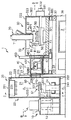
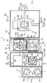
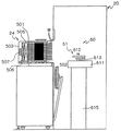
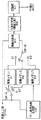
図1及び図2は、検査システム1の主要な構成要素を示す立面図及び平面図である。検査システム1は、複数枚のウエハを収納したカセットを保持するカセットホルダ10と、ミニエンバイロメント装置20と、主ハウジング30と、ミニエンバイロメント装置20と主ハウジング30との間に配置されていて、二つのローディングチャンバを画成するローダハウジング40と、ウエハをカセットホルダ10から主ハウジング30内に配置されたステージ装置50上に装填するローダ60と、主ハウジング30内に配置され、ウエハであるウエハWを載置して移動させるステージ装置50と、主ハウジング30に取り付けられた電子光学系70とを備え、それらは、図1及び図2に示したような位置関係で配置されている。検査システム1は、また、真空の主ハウジング30内に配置されたプレチャージユニット81と、ウエハに電位を印加する電位印加機構と、電子ビームキャリブレーション機構と、ステージ装置50上でのウエハの位置決めを行うためのアライメント制御装置87(図6に図示)を構成する光学顕微鏡871とを備えている。検査システム1はさらに、これらの要素の動作を制御するための制御装置2を備えている。
以下に、検査システム1の主要な要素(サブシステム)それぞれの構成について、詳細に説明する。
Before describing an embodiment of a defect inspection apparatus according to the present invention, an overall configuration of an inspection system for a semiconductor wafer that can be used by incorporating the defect inspection apparatus will be described.
FIGS. 1 and 2 are an elevation view and a plan view showing main components of the
Below, the structure of each of the main elements (subsystems) of the
カセットホルダ10
カセットホルダ10は、複数枚(例えば25枚)のウエハが上下方向に平行に並べられた状態で収納されたカセットc(例えば、アシスト社製のSMIF、FOUPのようなクローズドカセット)を複数個(この実施形態では2個のカセット)保持するようになっている。このカセットホルダとしては、カセットをロボット等により搬送して自動的にカセットホルダ10に装填する場合には、それに適した構造のものを、また人手により装填する場合には、それに適したオープンカセット構造のものを、それぞれ任意に選択して設置できるようになっている。カセットホルダ10は、この実施形態では、自動的にカセットcが装填される形式であり、例えば昇降テーブル11と、その昇降テール11を上下移動させる昇降機構12とを備えている。カセットcは、昇降テーブル上に図2において鎖線で示した状態に自動的に装填可能であり、装填後、図2において実線で示した状態に自動的に回転され、ミニエンバイロメント装置20内の第1の搬送ユニットの回動軸線に向けられる。また、昇降テーブル11は、図1において鎖線で示した状態に降下される。
Cassette holder 10
The
別の実施形態では、図3に示すように、複数の300mmウエハWを箱本体501の内側に固定した溝型ポケット(不図示)に収納した状態で収容し、搬送、保管等を行うものである。この基板搬送箱24は、角筒状の箱本体501と基板搬送出入り口ドアの自動開閉装置とに連結されて、箱本体501の側面の開口部を機械により開閉可能な基板搬送出入りドア502と、開口部と反対側に位置し、フィルタ類及びファンモータの着脱を行うための開口部を覆う蓋体503と、ウエハWを保持するための溝型ポケット507とから構成されている。この実施形態では、ローダー60のロボット式の搬送ユニット61により、ウエハを出し入れする。
なお、カセットc内に収納されるウエハは、半導体製造工程中でウエハを処理するプロセスの後、若しくはプロセスの途中で行われる。具体的には、成膜工程、CMP、イオン注入等を受けたウエハ、表面に配線パターンが形成されたウエハ、又は配線パターンが未だに形成されていないウエハが、検査のためにカセットc内に収納される。カセットc内に収容されるウエハは、多数枚上下方向に隔ててかつ平行に並べて配置されており、カセット中の任意の位置のウエハを、後述する第1の搬送ユニットで保持できるようにするために、第1の搬送ユニットのアームを上下移動できるようになっている。
In another embodiment, as shown in FIG. 3, a plurality of 300 mm wafers W are accommodated in a grooved pocket (not shown) fixed inside the
The wafer stored in the cassette c is performed after or during the process of processing the wafer in the semiconductor manufacturing process. Specifically, a wafer that has undergone a film formation process, CMP, ion implantation, a wafer with a wiring pattern formed on the surface, or a wafer that has not yet been formed with a wiring pattern is stored in a cassette c for inspection. Is done. A large number of wafers accommodated in the cassette c are arranged side by side in parallel in the vertical direction so that a wafer at an arbitrary position in the cassette can be held by a first transfer unit to be described later. In addition, the arm of the first transport unit can be moved up and down.
ミニエンバイロメント装置20
図4は、ミニエンバイロメント装置20を図1とは異なる方向から見た立面図である。この図4並びに先の図1及び図2に示したように、ミニエンバイロメント装置20は、雰囲気制御されるミニエンバイロメント空間21を画成するハウジング22と、ミニエンバイロメント空間21内で清浄空気等の気体を循環して雰囲気制御するための気体循環装置23と、ミニエンバイロメント空間21内に供給された空気の一部を回収して排出する排出装置24と、ミニエンバイロメント空間21内に配設されていて試料であるウエハの粗位置決めを行うプリアライナ25とを備えている。
FIG. 4 is an elevational view of the
ハウジング22は、頂壁221、底壁222及び四周を囲む周壁223を有し、ミニエンバイロメント空間21を外部から遮断する構造になっている。ミニエンバイロメント空間21を雰囲気制御するために、気体循環装置23は、図4に示されるように、ミニエンバイロメント空間21内において、頂壁221に下向きに取り付けられていて、気体(この実施形態では空気)を清浄にして一つ又はそれ以上の気体吹き出し口(図示せず)を通して清浄空気を真下に向かって層流状に流す気体供給ユニット231と、底壁222の上に配置されていて、底に向かって流れ下った空気を回収する回収ダクト232と、回収ダクト232と気体供給ユニット231とを接続して回収された空気を気体供給ユニット231に戻す導管233とを備えている。
The
清浄空気の層流状の下方向の流れすなわちダウンフローは、主に、ミニエンバイロメント空間21内に配置された後述する第1の搬送ユニットによる搬送面を通して流れるように供給され、これにより、搬送ユニットにより発生する恐れのある塵埃がウエハに付着するのを防止する。ハウジング22の周壁223のうち、カセットホルダ10に隣接する部分には、出入り口225が形成されている。
排出装置24は、後に説明する搬送ユニットのウエハ搬送面より下側の位置で搬送ユニットの下部に配置された吸入ダクト241と、ハウジング22の外側に配置されたブロワー242と、吸入ダクト241とブロワー242とを接続する導管243と、を備えている。この排出装置24は、搬送ユニットの周囲を流れ下り搬送ユニットにより発生する可能性のある塵埃を含んだ気体を、吸入ダクト241により吸引し、導管243、244及びブロワー242を介してハウジング22の外側に排出する。
The laminar flow of the clean air, that is, the downward flow, that is, the downward flow is mainly supplied so as to flow through a transfer surface by a first transfer unit (described later) disposed in the
The
ミニエンバイロメント空間21内に配置されたプリアライナー25は、ウエハに形成されたオリエンテーションフラット(円形のウエハの外周に形成された平坦部分を言い、以下においてオリフラと呼ぶ)や、ウエハの外周縁に形成された一つ又はそれ以上のV型の切欠きすなわちノッチを光学的に或いは機械的に検出し、それに基づいて、ウエハの軸線O1−O1の周りの回転方向の位置を、約±1度の精度で予め位置決めする。プリアライナー25は、ウエハであるウエハの座標を決める機構の一部を構成し、ウエハの粗位置決めを担当する。
The pre-aligner 25 disposed in the
主ハウジング30
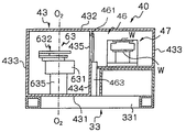
図1及び図2に示したように、ワーキングチャンバ31を画成する主ハウジング30は、ハウジング本体32を備え、そのハウジング本体32は、台フレーム36上に配置された振動遮断装置すなわち防振装置37の上に載せられたハウジング支持装置33によって支持されている。ハウジング支持装置33は矩形に組まれたフレーム構造体331を備えている。ハウジング本体32は、フレーム構造体331上に配設固定されており、フレーム構造体上に載せられた底壁321と、頂壁322と、底壁321及び頂壁322に接続されて四周を囲む周壁323とを備え、ワーキングチャンバ31を外部から隔離している。この実施形態においては、ハウジング32本体及びハウジング支持装置33は、剛構造に組み立てられていて、台フレーム36が設置されている床からの振動がこの剛構造に伝達されるのを、防振装置37で阻止している。ハウジング32の周壁323の内、ローダハウジング40に隣接する周壁には、ウエハ出し入れ用の出入り口325が形成されている。
As shown in FIGS. 1 and 2, the
ワーキングチャンバ31は、汎用の真空装置(図示せず)により、真空雰囲気に保たれる。台フレーム36の下には、検査システム1全体の動作を制御する制御装置2が配置されている。
なお、検査システム1においては、主ハウジング30を含めて、種々のハウジングを真空排気しているが、そのための真空排気系は、真空ポンプ、真空バルブ、真空ゲージ、真空配管等から構成され、電子光学系、検出器部、ウエハ室、ロードロック室等を、所定のシーケンスに従って真空排気を行う。各部においては、必要な真空度を達成するように、真空バルブが制御される。そして、常時、真空度の監視を行い、異常時には、インターロック機能により隔離バルブ等によるチャンバ間又はチャンバと排気系との間の遮断緊急制御を行い、各部において必要な真空度を確保をする。真空ポンプとしては、主排気にターボ分子ポンプ、粗引き用としてルーツ式のドライポンプを使用する。検査場所(電子線照射部)の圧力は、10−3〜10−5Pa、好ましくは、その1桁下の10−4〜10−6Paが実用的である。
The working
In the
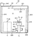
ローダハウジング40
図5は、図1とは別の方向から見たローダハウジング40の立面図を示している。図5並びに図1及び図2に示すように、ローダハウジング40は、第1のローディングチャンバ41と第2のローディングチャンバ42とを画成するハウジング本体43を備えている。ハウジング本体43は、底壁431と、頂壁432と、四周を囲む周壁433と、第1のローディングチャンバ41と第2のローディングチャンバ42とを仕切る仕切壁434とを有しており、2つのローディングチャンバを外部から隔離している。仕切壁434には、2つのローディングチャンバ間でウエハWの受け渡しを行うための開口すなわち出入り口435が形成されている。また、周壁433のミニエンバイロメント装置20及び主ハウジング30に隣接した部分には、出入り口436及び437が形成されている。このローダハウジング40のハウジング本体43は、ハウジング支持装置33のフレーム構造体331上に載置されて支持されている。したがって、このローダハウジング40にも、床の振動が伝達されない。
FIG. 5 shows an elevational view of the
ローダハウジング40の出入り口436とミニエンバイロメント装置20のハウジング22の出入り口226とは整合されているが、これら出入り口436、226の間には、ミニエンバイロメント空間21とローディングチャンバ41との連通を選択的に阻止するシャッタ装置27が設けられている。また、ローダハウジング40の出入り口437と主ハウジング30のハウジング本体32の出入り口325とは整合されているが、これら出入り口436、325の間には、ローディングチャンバ42とワーキンググチャンバ31との連通を選択的に密封阻止するシャッタ装置45が設けられている。更に、仕切壁434に形成された開口には、扉461により開口を閉じて、第1及び第2のローディングチャンバ間の連通を選択的に密封阻止するシャッタ装置46が設けられている。これらのシャッタ装置27、45及び46は、閉じ状態にあるとき、各チャンバを気密シールできるようになっている。
Although the entrance /
第1のローディングチャンバ41内には、複数枚(この実施形態では2枚)のウエハWを上下に隔てて水平に支持するウエハラック47が配設されている。
第1及び第2のローディングチャンバ41及び42は、真空ポンプを含む汎用の真空排気装置(図示せず)によって、高真空状態(真空度としては、10-5〜10-6Pa)に雰囲気制御される。この場合、第1のローディングチャンバ41を低真空チャンバとして低真空雰囲気に保ち、第2のローディングチャンバ42を高真空チャンバとして高真空雰囲気に保つことにより、ウエハの汚染防止を効果的に行うこともできる。このような2つのローディングチャンバを備えたローディングハウジング構造を採用することによって、ウエハWをローディングチャンバからワーキングチャンバ内に遅滞なく搬送することができる。このようなローディングチャンバ構造を採用することによって、欠陥等の検査のスループットを向上させ、更に、保管状態が高真空状態であることを要求される電子源周辺の真空度を、可能な限り高真空状態にすることができる。
In the first loading chamber 41, a
The first and
第1及び第2のローディングチャンバ41及び42にはそれぞれ、真空排気配管と不活性ガス(例えば乾燥純窒素)用のベント配管(それぞれ図示せず)が接続されている。これによって、各ローディングチャンバ内の大気圧状態において、不活性ガスベント(不活性ガスを注入して、不活性ガス以外の酸素ガス等が表面に付着するのを防止する)が達成される。
なお、電子線を使用する本発明の主ハウジング30において、電子光学系70の電子源すなわち電子銃として使用される代表的な六硼化ランタン(LaB6)等は、一度熱電子を放出する程度まで高温状態に加熱された場合には、酸素等に可能な限り接触させないことがその寿命を縮めないために肝要である。本発明においては、主ハウジング30の電子光学系70が配置されているワーキングチャンバにウエハWを搬入する前段階で、上記のような雰囲気制御を行うことにより、酸素に接触する可能性が低減されるため、電子源の寿命を縮めてしまう可能性が低くなる。
A vacuum exhaust pipe and a vent pipe (not shown) for an inert gas (for example, dry pure nitrogen) are connected to the first and
In the
ステージ装置50
ステージ装置50は、主ハウジング30の底壁321上に配置された固定テーブル51と、固定テーブル上でY方向(図1において紙面に垂直の方向)に移動するYテーブル52と、Yテーブル上でX方向(図1において左右方向)に移動するXテーブル53と、Xテーブル上で回転可能な回転テーブル54と、回転テーブル54上に配置されたホルダ55とを備えている。該ホルダ55のウエハ載置面551上にウエハWを解放可能に保持する。ホルダ55は、ウエハWを機械的に或いは静電チャック方式で解放可能に把持できる汎用の構造のものでよい。ステージ装置50は、サーボモータ、エンコーダ及び各種のセンサ(図示せず)を用いて、上記した複数のテーブル52〜54を動作させることにより、載置面551上でホルダ55に保持されたウエハWを電子光学系70から照射される電子ビームに対してX方向、Y方向及びZ方向(図1において上下方向)に、更には、ウエハの支持面に鉛直な軸線の回り方向(θ方向)に、高い精度で位置決めすることができる。
The
なお、Z方向の位置決めは、例えばホルダ55上の載置面の位置をZ方向に微調整可能にしておけばよい。この場合、載置面の参照位置を微細径レーザによる位置測定装置(干渉計の原理を使用したレーザ干渉測距装置)によって検知し、その位置をフィードバック回路(不図示)によって制御したり、それと共に或いはそれに代えて、ウエハのノッチ或いはオリフラの位置を測定して、ウエハの電子ビームに対する平面位置及び回転位置を検知し、回転テーブル54を微小角度制御可能なステッピングモータなどにより回転させて制御する。ホルダ55を設けずに、回転テーブル54上にウエハWを直接載置してもよい。ワーキングチャンバ31内での塵埃の発生を極力防止するために、ステージ装置50用のサーボモータ521、531及びエンコーダ522、532は、主ハウジング30の外側に配置されている。
電子ビームに対するウエハWの回転位置やX−Y座標位置を、後述する信号検出系或いは画像処理系に予め入力することによって、信号の参照化を図ることもできる。
The positioning in the Z direction may be performed by finely adjusting the position of the mounting surface on the
By inputting the rotation position of the wafer W with respect to the electron beam and the XY coordinate position in advance into a signal detection system or an image processing system, which will be described later, the signal can be referenced.
ローダ60
ローダ60は、ミニエンバイロメント装置20のハウジング22内に配置されたロボット式の第1の搬送ユニット61と、第2のローディングチャンバ42内に配置されたロボット式の第2の搬送ユニット63とを備えている。
第1の搬送ユニット61は、駆動部611に関して軸線O1−O1の回りで回転可能になっている多節のアーム612を有している。多節のアームとして任意の構造のものを使用できるが、この実施形態では、互いに回動可能に取り付けられた三つの部分を有している。第1の搬送ユニット61のアーム612の一つの部分すなわち最も駆動部611側の第1の部分は、駆動部611内に設けられた汎用構造の駆動機構(図示せず)により、回転可能な軸613に取り付けられている。アーム612は、軸613により軸線O1−O1の回りで回動可能であると共に、部分間の相対回転により全体として軸線O1−O1に関して半径方向に伸縮可能である。アーム612の軸613から最も離れた第3の部分の先端には、汎用構造の機械式チャック又は静電チャック等のウエハ把持用の把持装置616が設けられている。駆動部611は、汎用構造の昇降機構615により上下方向に移動可能である。
The
The
この第1の搬送ユニット61において、カセットホルダ10中に保持された二つのカセットcの内のいずれか一方の方向M1又はM2(図2)に向かって、アーム612が伸び、そして、カセットc内に収容されたウエハWをアームの上に載せるか又はアームの先端に取り付けたチャック(図示せず)により把持して取り出す。その後、アームが縮み(図2に示した状態)、アームがプリアライナ25の方向M3に向かって伸長できる位置まで回転して、その位置で停止する。するとアームが再び伸びてアームに保持されたウエハWをプリアライナ25に載せる。プリアライナ25から前記と逆にしてウエハを受け取った後、アームは更に回転し、第1のローディングチャンバ41に向かって伸長できる位置(向きM4)で停止し、第1のローディングチャンバ41内のウエハ受け47に、ウエハを受け渡す。なお、機械的にウエハを把持する場合には、ウエハの周縁部(周縁から約5mmの範囲)を把持する。これは、ウエハには周縁部を除いて全面にデバイス(回路配線)が形成されており、周縁部以外の部分を把持すると、デバイスの破壊、欠陥の発生を生じさせるからである。
第2の搬送ユニット63も、第1の搬送ユニット61と構造が基本的に同じであり、ウエハWの搬送を、ウエハラック47とステージ装置50の載置面上との間で行う点でのみ相違する。
In the
The
第1及び第2の搬送ユニット61及び63は、カセットホルダに保持されたカセットcからワーキングチャンバ31内に配置されたステージ装置50上への及びその逆のウエハの搬送を、ウエハをほぼ水平状態に保ったままで行う。そして、搬送ユニット61、63のアームが上下動するのは、単に、カセットcからのウエハの取り出し及びそれへの挿入、ウエハラックへのウエハの載置及びそこからの取り出し、並びに、ステージ装置50へのウエハの載置及びそこからの取り出しのときるだけである。したがって、例えば直径30cm等の大型のウエハであっても、その移動をスムースに行うことができる。
ここで、上記構成を有する検査システム1において、カセットホルダ10に支持されたカセットcからワーキングチャンバ31内に配置されたステージ装置50までへのウエハの搬送を、順を追って説明する。
The first and
Here, in the
カセットホルダ10は、前述のように人手によりカセットをセットする場合にはそれに適した構造のものが、また自動的にカセットをセットする場合にはそれに適した構造のものが使用される。この実施形態において、カセットcがカセットホルダ10の昇降テーブル11の上にセットされると、昇降テーブル11は昇降機構12によって降下され、カセットcが出入り口225に整合される。カセットが出入り口225に整合されると、カセットcに設けられたカバー(不図示)が開き、また、カセットcとミニエンバイロメント装置20の出入り口225との間には、筒状の覆いが配置されて、カセット及びミニエンバイロメント空間21を、外部から遮断する。なお、ミニエンバイロメント装置20側に出入り口225を開閉するシャッタ装置が設けられている場合には、そのシャッタ装置が動作して、出入り口225を開く。
As described above, the
一方、第1の搬送ユニット61のアーム612は、方向M1又はM2のいずれかに向いた状態(この説明では、M1の方向)で停止しており、出入り口225が開くと、アームが伸びてその先端でカセットcに収容されているウエハのうち1枚を受け取る。
アーム612によるウエハの受け取りが完了すると、該アームは縮み、シャッタ装置が動作して出入り口を閉じ(シャッタ装置がある場合)、次に、アーム612は軸線O1−O1の回りで回動し、方向M3に向けて伸長できる状態となる。そして、アームが伸びて先端に載せられ或いはチャックで把持されたウエハをプリアライナ25の上に載せ、該プリアライナによって、ウエハの回転方向の向き(ウエハ平面に垂直な中心軸線の回りの向き)を、所定の範囲内に位置決めする。位置決めが完了すると、第1の搬送ユニット61は、アーム612の先端にプリアライナ25からウエハを受け取った後にアームを縮ませ、方向M4に向けてアームを伸長できる姿勢になる。すると、シャッタ装置27の扉272が動いて出入り口226及び436を開き、アーム612が伸びてウエハを第1のローディングチャンバ41内のウエハラック47の上段側又は下段側に載せる。なお、シャッタ装置27が開いてウエハラック47にウエハが受け渡される前に、仕切壁434に形成された開口435は、シャッタ装置46の扉461により気密状態に閉じられている。
On the other hand, the
When the reception of the wafer by the
上記した第1の搬送ユニット61によるウエハの搬送過程において、ミニエンバイロメント装置20のハウジング本体22に設けられた気体供給ユニット231からは清浄空気が層流状に流れ(ダウンフローとして)、搬送途中で塵埃がウエハの上面に付着するのを防止する。搬送ユニット周辺の空気の一部(この実施形態では、供給ユニットから供給される空気の約20%で主に汚れた空気)は、排出装置24の吸入ダクト241から吸引されて、ハウジング外に排出される。残りの空気は、ハウジング本体22の底部に設けられた回収ダクト232を介して回収され、再び気体供給ユニット231に戻される。
In the wafer transfer process by the
ローダハウジング40の第1のローディングチャンバ41内のウエハラック47に第1の搬送ユニット61によりウエハが載せられると、シャッタ装置27が閉じて、ローディングチャンバ41を密閉する。すると、該ローディングチャンバ41内には空気が追い出されて不活性ガスが充填された後、その不活性ガスも排出されて、ローディングチャンバ41内は真空雰囲気となる。ローディングチャンバ41の真空雰囲気は、低真空度でよい。ローディングチャンバ41の真空度がある程度得られると、シャッタ装置46が動作して、扉461で密閉していた出入り口434を開き、次いで、第2の搬送ユニット63のアーム632が伸びて先端の把持装置でウエハ受け47から1枚のウエハを受け取る(先端の上に載せて或いは先端に取り付けられたチャックで把持して)。ウエハの受け取りが完了するとアームが縮み、シャッタ装置46が再び動作して扉461により出入り口435を閉じる。なお、シャッタ装置46が開く前に、アーム632は予めウエハラック47の方向N1に向けて伸長できる姿勢になる。また、前記のように、シャッタ装置46が開く前に、シャッタ装置45の扉452により出入り口437、325を閉じて、第2のローディングチャンバ42内とワーキングチャンバ31内との連通を阻止しており、かつ、第2のローディングチャンバ42内は真空排気される。
When a wafer is placed on the
シャッタ装置46が出入り口435を閉じると、第2のローディングチャンバ42は再度真空排気され、第1のローディングチャンバ41よりも高真空度で真空にされる。その間に、第2の搬送ユニット61のアームは、ワーキングチャンバ31内のステージ装置50の方向に向いて伸長できる位置に回転される。一方ワーキングチャンバ31内のステージ装置50では、Yテーブル52が、Xテーブル53の中心線X0−X0が第2の搬送ユニット63の回動軸線O2−O2を通るX軸線X1−X1とほぼ一致する位置まで、図2で上方に移動し、また、Xテーブル53が図2で最も左側の位置に接近する位置まで移動し、この状態で待機している。第2のローディングチャンバ42がワーキングチャンバ31の真空状態と略同じになると、シャッタ装置45の扉452が動いて出入り口437、325を開き、アームが伸びて、ウエハを保持したアームの先端がワーキングチャンバ31内のステージ装置50に接近する。そして、ステージ装置50の載置面551上にウエハWを載置する。ウエハの載置が完了するとアームが縮み、シャッタ装置45が出入り口437、325を閉じる。
When the
以上は、カセットc内のウエハWをステージ装置50の載置面551上に搬送載置するまでの動作に付いて説明した。検査処理が完了したウエハWをステージ装置50からカセットcに戻すには、前述と逆の動作を行う。また、ウエハラック47に複数のウエハを載置しているため、第2の搬送ユニット63がウエハラック47とステージ装置50との間でウエハの搬送を行っている間に、第1の搬送ユニットがカセットcとウエハラック47との間でウエハの搬送を行うことができる。したがって、検査処理を効率良く行うことができる。
The operation until the wafer W in the cassette c is transferred and placed on the
電子光学系70
電子光学系70は、試料の画像を得るための系であり、試料に電子線を衝突させ、試料から放出された二次電子、反射電子、後方散乱電子を検出して試料の画像を生成するSEM装置又は写像投影型の任意の電子線装置を使用可能である。このような電子線装置を用いることにより、分解能を向上させることができる。なお、検出される電子は、試料の表面の情報を保持しているものであれば何でもよく、例えば、試料の表面付近に逆電界を形成することにより、試料に直接衝突せずに、試料付近で反射するミラー電子(広義には反射電子とも言う)、或いは試料を透過する透過電子等でもよい。特に、ミラー電子を用いた場合には、電子が試料に直接衝突しないので、チャージアップの影響が極めて小さいという利点がある。
ミラー電子を利用する場合には、試料に、加速電圧よりも低い負の電位を印加し、試料付近に逆電界を形成する。この負の電位は、試料の表面付近で殆どの電子線が戻される程度の値に設定するのがよい。具体的には、電子銃の加速電圧よりも0.5〜1.0V以上低い電位に設定すればよい。例えば、加速電圧が−4kVの場合、試料への印加電圧は−4.000kV〜−4.050kVに設定するのが好ましい。更に望ましくは、−4.0005kV〜−4.020kVがよく、更に好ましくは−4.0005kV〜−4.010kVに設定するのが好適である。
他に、電子線ではないが、X線も利用してもよい。
Electron
The electron
When mirror electrons are used, a negative potential lower than the acceleration voltage is applied to the sample to form a reverse electric field near the sample. This negative potential is preferably set to such a value that most of the electron beam is returned near the surface of the sample. Specifically, it may be set to a potential lower by 0.5 to 1.0 V or more than the acceleration voltage of the electron gun. For example, when the acceleration voltage is −4 kV, the voltage applied to the sample is preferably set to −4.00 kV to −4.050 kV. More desirably, it is preferably −4.005 kV to −4.020 kV, and more preferably −4.005 kV to −4.010 kV.
In addition, although not an electron beam, an X-ray may be used.
プレチャージユニット81
プレチャージユニット81は、図1に示したように、ワーキングチャンバ31内で電子光学系70の鏡筒71に隣接して配設されている。本発明の検査システム1では、ウエハに電子線を走査して照射することによってウエハ表面に形成されたデバイスパターン等を検査する形式の装置であるため、ウエハ材料、照射電子のエネルギ等の条件によって、ウエハ表面が帯電(チャージアップ)することがある。更に、ウエハ表面でも強く帯電する箇所、弱い帯電箇所が生じる可能性がある。そして、電子線の照射により生じる二次電子等の情報をウエハ表面の情報としているが、ウエハ表面の帯電量にむらがあると、二次電子の情報もむらを含み、正確な画像を得ることができない。そこで、この実施形態では、帯電むらを防止するために、プレチャージユニット81が設けられている。該プレチャージユニット81は荷電粒子照射部811を含み、ウエハ上に検査のために一次電子を照射する前に、荷電粒子照射部811から荷電粒子を照射することにより、帯電むらを無くす。なお、ウエハ表面の帯電状態は、電子光学系70を用いて予めウエハ面の画像を形成し、その画像を評価することで検出することができ、そして、検出された帯電状態に基づいて、荷電粒子照射部811からの荷電粒子の照射を制御する。プレチャージユニット81では、一次電子線をぼかして照射してもよい。
As shown in FIG. 1, the
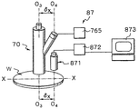
アライメント制御装置87
アライメント制御装置87は、ステージ装置50を用いてウエハWを電子光学系70に対して位置決めさせる装置である。アライメント制御装置87は、光学顕微鏡871(図1)を用いた広視野観察によるウエハの概略位置合わせである低倍率合わせ(電子光学系によるよりも倍率が低い位置合わせ)、電子光学系70の電子光学系を用いたウエハの高倍率合わせ、焦点調整、検査領域設定、パターンアライメント等の制御を行うようになっている。なお、このように低倍率でウエハを検査するのは、ウエハのパターンの検査を自動的に行うためには、電子線を用いた狭視野でウエハのパターンを観察してウエハライメントを行うときに、電子線によるアライメントマークを容易に検出する必要があるからである。
The
光学顕微鏡871は、主ハウジング30内に設けられているが、主ハウジング30内で移動可能に設けられていてもよい。光学顕微鏡871を動作させるための光源(不図示)も主ハウジング30内に設けられている。また高倍率の観察を行う電子光学系は、電子光学系70の電子光学系(一次光学系72及び二次光学系74)を共用するものである。
図6は、アライメント制御装置87の概略構成を示している。ウエハW上の被観察点を低倍率で観察するには、ステージ装置50のXステージ又はYステージを動かすことによって、ウエハの被観察点を光学顕微鏡の視野内に移動させる。光学顕微鏡871を用いて広視野でウエハを視認し、そのウエハ上の観察すべき位置をCCD872を介してモニタ873に表示させ、観察位置すなわち被観察点の位置を、おおよそ決定する。この場合、光学顕微鏡871の倍率を低倍率から高倍率に徐々に変化させるようにしてもよい。
The
FIG. 6 shows a schematic configuration of the
次に、ステージ装置50を電子光学系70の光軸と光学顕微鏡871の光軸との間隔δxに相当する距離だけ移動させることにより、光学顕微鏡871を用いて予め決めたウエハ上の被観察点を電子光学系70の視野位置に移動させる。この場合、電子光学系70の軸線O3−O3と光学顕微鏡871の光軸O4−O4との間の距離(この実施形態では、X軸方向にのみ両者は位置ずれしているものとするが、Y軸方向に位置ずれしていてもよい)δxは予めわかっているので、その値δxだけ移動させれば、被観察点を視認位置に移動させることができる。電子光学系70の視認位置への被観察点の移動が完了した後、電子光学系により高倍率で被観察点をSEM撮像して画像を記憶したり、モニタ873に表示させる。
Next, the
このようにして、電子光学系によって高倍率でウエハの観察点をモニタに表示させた後、公知の方法により、ステージ装置50の回転テーブル54の回転中心に関するウエハの回転方向の位置ずれ、すなわち電子光学系の光軸O3−O3に対するウエハの回転方向のずれθを検出し、また電子光学系70に関する所定のパターのX軸及びY軸方向の位置ずれを検出する。そして、その検出値並びに別途得られたウエハに設けられた検査マークのデータ、或いはウエハのパターンの形状等に関するデータに基づいて、ステージ装置50の動作を制御してウエハのアライメントを行う。
In this way, after the observation point of the wafer is displayed on the monitor at a high magnification by the electron optical system, the positional deviation of the rotation direction of the wafer with respect to the rotation center of the rotary table 54 of the
制御装置2
制御装置2の制御系は、主に、メインコントローラ、制御コントローラ、ステージコントローラから構成されている。
メインコントローラには、マン−マシンインターフェースが備えられており、オペレータの操作は、ここを通して行われる(種々の指示/命令、レシピなどの入力、検査スタートの指示、自動と手動検査モードの切り替え、手動検査モード時等の必要な全てのコマンドの入力等)。その他、工場のホストコンピュータとのコミュニケーション、真空排気系の制御、ウエハの搬送、位置合わせの制御、制御コントローラやステージコントローラヘのコマンドの伝達や情報の受け取り等も、メインコントローラで行われる。また、光学顕微鏡からの画像信号の取得、ステージの変動信号を電子光学系にフィードバックさせて像の悪化を補正するステージ振動補正機能、ウエハ観察位置のZ軸方向(二次光学系の軸方向)の変位を検出して、電子光学系ヘフィードバツクし、自動的に焦点を補正する自動焦点補正機能を備えている。電子光学系へのフィードバック信号等の授受、及びステージ装置からの信号の授受は、それぞれ制御コントローラ及びステージコントローラを介して行われる。
The control system of the
The main controller is provided with a man-machine interface through which operator operations are performed (various instructions / commands, recipe input, inspection start instructions, automatic and manual inspection mode switching, manual operation, etc. Input all necessary commands in inspection mode etc.). In addition, communication with the host computer in the factory, control of the evacuation system, wafer transfer, alignment control, transmission of commands to the control controller and stage controller, reception of information, and the like are also performed by the main controller. Also, acquisition of image signal from optical microscope, stage vibration correction function that feeds back stage fluctuation signal to electron optical system to correct image deterioration, wafer observation position Z-axis direction (axial direction of secondary optical system) And an automatic focus correction function for automatically correcting the focus by detecting the displacement of the lens and feeding back to the electron optical system. Transmission / reception of feedback signals and the like to the electron optical system and transmission / reception of signals from the stage apparatus are performed via a control controller and a stage controller, respectively.
制御コントローラは、主に電子光学系70の制御、すなわち、電子銃、レンズ、アライナー、ウィーンフィルタ用等の高精度電源の制御等を担う。具体的には、照射領域に、倍率が変わったときにも常に一定の電子電流が照射されるように電源を制御すること、各倍率に対応した各レンズ系やアライナーへ自動的に電圧を設定すること等の、各オペレーションモードに対応した各レンズ系やアライナーへの自動電圧設定等の制御(連動制御)が行われる。
ステージコントローラは、主にステージの移動に関する制御を行い、精密なX軸方向およびY軸方向のμmオーダーの移動(±0.5μm程度の許容誤差)を可能にしている。また、ステージの移動制御では、誤差精度±0.3秒程度以内で、回転方向の制御(θ制御)も行われる。
The control controller is mainly responsible for the control of the electron
The stage controller mainly controls the movement of the stage and enables precise movement in the order of μm in the X-axis direction and Y-axis direction (allowable error of about ± 0.5 μm). In stage movement control, rotation direction control (θ control) is also performed within an error accuracy of about ± 0.3 seconds.
検査システム1はさらに、電子光学系70によって得られたデータを処理して画像データを取得し、得られた画像データに基づいてウエハ上の欠陥を検出する欠陥検査装置を備えている。以下に、本発明に係る半導体ウエハの欠陥検査装置について説明する。
なお、一般に、電子線を用いた検査装置すなわち電子光学系70は、高価であり、またスループットも他のプロセス装置に比べて低い。そのため、現状では最も検査が必要と考えられている重要な工程(例えばエッチング、成膜、又はCMP(化学機械研磨)平坦化処理等)の後に、また、配線工程ではより微細な配線工程部分、すなわち配線工程の1から2工程、及び前工程のゲート配線工程等に利用されている。特に、デザインルールが100nm以下、即ち、100nm以下の線幅を有する配線や直径100nm以下のビアホール等の形状欠陥や電気的欠陥を見つけ、また、プロセスにフィードバックすることが重要である。
The
In general, an inspection apparatus using an electron beam, that is, an electron
上記したように、検査されるウエハは大気搬送系及び真空搬送系を通して、超精密のステージ装置(X−Yステージ)50上に位置合わせ後、静電チャック機構等により固定される。そして、欠陥検査工程では、光学顕微鏡により、必要に応じて各ダイの位置確認や、各場所の高さ検出が行われ、記憶される。光学顕微鏡は、この他に欠陥等の見たい所の光学顕微鏡像を取得し、電子線像との比較等にも使用される。次に電子光学系の条件設定を行い、電子線像を用いて、光学顕微鏡で設定された情報の修正を行い、精度を向上させる。
次いで、ウエハの種類(どの工程後か、ウエハのサイズは200mmか300mmか等)に応じたレシピの情報を装置に入力し、以下、検査場所の指定、電子光学系の設定、検査条件の設定等を行なった後、画像取得を行ないながら通常はリアルタイムで欠陥検査を行なう。セル同士の比較、ダイ比較等が、アルゴリズムを備えた高速の情報処理システムにより検査が行なわれ、必要に応じてCRT等に結果を出力や、メモリへ記憶を行なう。
As described above, the wafer to be inspected is positioned on the ultra-precision stage device (XY stage) 50 through the atmospheric transfer system and the vacuum transfer system, and then fixed by the electrostatic chuck mechanism or the like. In the defect inspection process, the position of each die and the height of each location are detected and stored by an optical microscope as necessary. In addition to this, the optical microscope obtains an optical microscope image of a desired location such as a defect and is used for comparison with an electron beam image. Next, the conditions of the electron optical system are set, and the information set by the optical microscope is corrected using the electron beam image to improve the accuracy.
Next, recipe information corresponding to the type of wafer (after which process, whether the wafer size is 200 mm or 300 mm, etc.) is input to the apparatus. Hereinafter, the designation of the inspection location, the setting of the electron optical system, and the setting of the inspection conditions After performing the above, defect inspection is normally performed in real time while acquiring an image. Cell-to-cell comparison, die comparison, and the like are inspected by a high-speed information processing system equipped with an algorithm, and the results are output to a CRT or the like or stored in a memory as necessary.
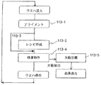
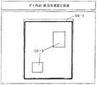
欠陥検査の基本的流れを、図7に示す。まずアライメント動作113・1を含んだウエハ搬送の後、検査に関係する条件等を設定したレシピを作成する(113・2)。レシピは被検査ウエハに最低1種類は必要であるが、複数の検査条件に対応するために、1枚の被検査ウエハに対して、複数のレシピが存在する場合もある。また同一パターンの被検査ウエハが複数枚ある場合、一種類のレシピで複数のウエハを検査する場合もある。図7の経路113・3は、この様に過去に作成されたレシピで検査する場合、検査動作直前にレシピの作成が不要であることを示している。
図7において、検査動作113・4は、レシピに記載された条件、シーケンスに従い、ウエハの検査を行う。欠陥抽出は、検査動作中に欠陥を発見する度に即時行われ、以下の動作をほぼ並列的に実行する。
・欠陥分類(113・5)を行い、結果出力ファイルに抽出欠陥情報と欠陥分類情報を追加する動作
・抽出欠陥画像を画像専用結果出力ファイルもしくはファイルに追加する動作
・抽出欠陥の位置などの欠陥情報を操作画面上に表示する動作
The basic flow of defect inspection is shown in FIG. First, after carrying the wafer including the alignment operation 113. 1, a recipe in which conditions relating to the inspection are set is created (113. 2). At least one type of recipe is required for the wafer to be inspected, but there may be a plurality of recipes for one wafer to be inspected in order to cope with a plurality of inspection conditions. Further, when there are a plurality of wafers to be inspected with the same pattern, a plurality of wafers may be inspected with one type of recipe. The path 1113 in FIG. 7 indicates that when the inspection is performed with the recipe created in the past, it is not necessary to create a recipe immediately before the inspection operation.
In FIG. 7, the inspection operation 1113 performs a wafer inspection according to the conditions and sequence described in the recipe. The defect extraction is performed immediately every time a defect is found during the inspection operation, and the following operations are executed in almost parallel.
・ Operation to perform defect classification (113/5) and add extracted defect information and defect classification information to result output file ・ Operation to add extracted defect image to image-only result output file or file ・ Defects such as position of extracted defect Operation to display information on the operation screen
被検査ウエハ単位で検査が終了すると、次いで、以下の動作をほぼ並列的に実行する。
・結果出力ファイルをクローズして保存する動作
・外部からの通信が検査結果を要求する場合、検査結果を送る動作
・ウエハを排出する動作
連続的にウエハを検査する設定がなされている場合、次の被検査ウエハを搬送して、前記一連の動作を繰り返す。
When the inspection is completed in units of wafers to be inspected, the following operations are then executed substantially in parallel.
・ Operation to close and save result output file ・ Operation to send inspection result when communication from outside requests inspection result ・ Operation to eject wafer When next wafer is set to be inspected continuously The wafer to be inspected is transferred, and the above series of operations is repeated.
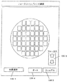
図7におけるレシピ作成においては、検査に関係する条件等の設定ファイルからなるレシピを作成する。該レシピは、保存することも可能であり、該レシピを使用して、検査時もしくは検査前に条件設定を行う。レシピに記載された検査に関係する条件は、例えば、以下の事項を含んでいる。
・検査対象ダイ
・ダイ内部検査領域
・検査アルゴリズム
・検出条件(検査感度等、欠陥抽出に必要な条件)
・観察条件(倍率、レンズ電圧、ステージ速度、検査順序等、観察に必要な条件)
In creating a recipe in FIG. 7, a recipe including a setting file for conditions related to inspection is created. The recipe can be stored, and conditions are set at the time of inspection or before inspection using the recipe. Conditions relating to the inspection described in the recipe include, for example, the following matters.
・ Die to be inspected ・ Die internal inspection area ・ Inspection algorithm ・ Detection condition
・ Observation conditions (magnification, lens voltage, stage speed, inspection order, etc.)
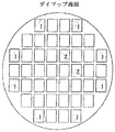
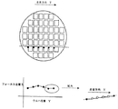
上記した検査条件の内、検査対象ダイの設定は、図8に示すように操作画面に表示されたダイマップ画面に対して、検査するダイをオペレータが指定する。図8の例では、ウエハ端面のダイ1と前工程で明らかに不良と判定されたダイ2をグレイアウトして検査対象から削除し、残りを検査対象ダイとしている。また、ウエハ端面からの距離や前工程で検出されたダイの良否情報をもとに、自動的に検査ダイを指定する機能も有している。
Among the inspection conditions described above, the inspection target die is set by the operator specifying a die to be inspected on the die map screen displayed on the operation screen as shown in FIG. In the example of FIG. 8, the
また、ダイ内部の検査領域の設定は、図9に示される様に操作画面に表示されたダイ内部検査領域設定画面に対して、検査領域をオペレータが光学顕微鏡もしくはEB顕微鏡により取得した画像をもとに、マウス等の入力機器で指定する。図9の例では、実線で示した領域115・1と破線で示した領域115・2を設定している。
領域115・1は、ダイのほぼ全体を設定領域としている。この場合、検査アルゴリズムは、隣接ダイ比較法とし、この領域に対する検出条件、観察条件の詳細は、別に設定する。領域115・2は、検査アルゴリズムをアレイ検査としこの領域に対する検出条件及び観察条件の詳細は、別に設定する。すなわち複数の検査領域の設定が可能でかつ、検査領域は、それぞれ独自の検査アルゴリズムや検査感度を条件設定できる。ただし、検査領域が重ね合った場合は、予め設定した優先順位の検査アルゴリズムを処理する。図9の例においては、領域115.2は、アレイ検査を行い、隣接ダイ比較検査は行われない。
In addition, as shown in FIG. 9, the setting of the inspection area inside the die includes an image obtained by the operator using an optical microscope or an EB microscope with respect to the inspection area setting screen displayed on the operation screen. And using an input device such as a mouse. In the example of FIG. 9, a
In the
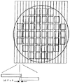
図7の検査動作においては、図10に示すように、被検査ウエハを走査幅に細分化して走査する。走査幅は、ほぼラインセンサの長さで決まるが、ラインセンサの端部が少し重なる様に設定してある。これは、検出した欠陥を最終的に統合処理する場合に、ライン間の連続性を判断する為や比較検査を行う際に画像アライメントするための余裕を確保するためである。その重ね量は、2048ドットのラインセンサに対して16ドット程度である。
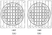
走査方向及びシーケンスを、模式的に図11に示す。すなわち、検査時間短縮のために双方向動作(A動作)や、機械制限からの単方向動作(B動作)などが、オペレータより選択できる構成になっている。
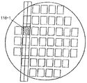
また、レシピの検査対象ダイ設定を元に、走査量を減らす動作を自動演算して検査する機能も有している。図12−1は検査ダイが1個のみの場合の走査例であり、不要な走査は行わない。
In the inspection operation of FIG. 7, as shown in FIG. 10, the wafer to be inspected is scanned by subdividing it into scanning widths. The scanning width is substantially determined by the length of the line sensor, but is set so that the end portions of the line sensor slightly overlap. This is to ensure a margin for image alignment when determining the continuity between lines or when performing a comparative inspection when the detected defects are finally integrated. The amount of overlap is about 16 dots for a 2048-dot line sensor.
The scanning direction and sequence are schematically shown in FIG. That is, in order to shorten the inspection time, a bidirectional operation (A operation) and a unidirectional operation (B operation) due to machine limitations can be selected by the operator.
In addition, it has a function of automatically calculating and inspecting an operation for reducing the scanning amount based on the inspection target die setting of the recipe. FIG. 12A is an example of scanning when there is only one inspection die, and unnecessary scanning is not performed.
レシピによって設定される検査アルゴリズムは、セル検査(アレイ検査)とダイ検査(ランダム検査)に大別することができる。
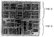
図12−2に示すように、ダイは、主にメモリに用いられる周期構造をしたセル部118・2と、周期構造を取らないランダム部118・3とに分けられる。周期構造をしたセル部118・2は、比較対象が同じダイの中に複数個あるので、セル検査、すなわち同じダイの中のセル同士で比較を行うことによって検査可能である。一方、ランダム部118・3は、同じダイの中に比較対象がないので、ダイ検査によってダイ同士の比較を行う必要がある。
ダイ検査は、比較対象により、さらに以下にように区分される。
・隣接ダイ比較法(Die-to-Die検査)
・基準ダイ比較法(Die-to- Any Die検査)
・CADデータ比較法(CAD Data-to-Any Die検査)
一般にゴールデンテンプレート方式と呼ばれる方式は、基準ダイ比較法及びCADデータ比較法であり、基準ダイ比較法においては、参照ダイをゴールデンテンプレートとし、CADデータ比較法おいては、CADデータをゴールデンテンプレートとする。
The inspection algorithm set by the recipe can be roughly divided into cell inspection (array inspection) and die inspection (random inspection).
As shown in FIG. 12B, the die is divided into a cell portion 118.2 having a periodic structure mainly used for a memory and a random portion 118.3 having no periodic structure. Since there are a plurality of comparison objects in the same die, the
The die inspection is further classified as follows according to the comparison target.
・ Adjacent die comparison method (Die-to-Die inspection)
・ Standard die comparison method (Die-to-Any Die inspection)
・ CAD data comparison method (CAD Data-to-Any Die inspection)
A method generally referred to as a golden template method is a standard die comparison method and a CAD data comparison method. In the standard die comparison method, a reference die is a golden template, and in a CAD data comparison method, CAD data is a golden template. .
以下に、各検査アルゴリズムの動作を述べる。
セル検査(アレイ検査)
セル検査は、周期構造の検査に適用される。DRAMセルなどはその一例である。
検査は、参照とする参照画像と被検査画像の比較を行い、その差分を欠陥として抽出する。参照画像と被検査画像は、二値化画像でも検出精度を向上するため多値画像でも構わない。
欠陥は、参照画像と被検査画像の差分そのものでも良いが、検出した差分の差分量や差分のある画素の合計面積などの差分情報を元にして、誤検出を防ぐための2次的な判定を行っても良い。
The operation of each inspection algorithm is described below.
Cell inspection (array inspection)
Cell inspection is applied to inspection of periodic structures. An example is a DRAM cell.
In the inspection, the reference image to be referred to is compared with the image to be inspected, and the difference is extracted as a defect. The reference image and the image to be inspected may be a binary image or a multi-value image in order to improve detection accuracy.
The defect may be the difference itself between the reference image and the image to be inspected, but it is a secondary determination for preventing erroneous detection based on difference information such as the difference amount of the detected difference and the total area of the pixels having the difference. May be performed.
セル検査においては、参照画像と被検査画像の比較は構造周期単位で行われる。すなわちCCDなどで一括取得した画像を読み出しながら1構造周期単位で比較しても良いし、参照画像がn個の構造周期単位であれば、n個の構造周期単位を同時に比較できる。
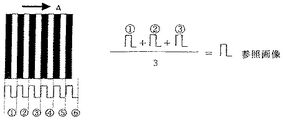
参照画像の生成方法の一例を図13に示す、ここでは1構造周期単位で比較する例を述べるので1構造周期単位生成を表す。同じ方法で周期数をnにする事も可能である。
前提として図13での検査方向はAである。また周期4を被検査周期とする。周期の大きさはオペレータが画像を見ながら入力するので、図13において周期1〜6は容易に認識できる。
参照周期画像は、各画素において被検査周期直前の周期1〜3を加算し平均して生成する。1〜3いずれかに欠陥が存在しても平均処理されるので影響は少ない。この形成された参照周期画像と被検査周期画像4を比較して欠陥の抽出を行う。
次に被検査周期画像5を検査する場合、周期2〜4を加算平均して参照周期画像を生成する。以下同様に被検査周期画像取得以前に得た画像より、被検査周期画像を生成して検査を連続させる。
In the cell inspection, the comparison between the reference image and the image to be inspected is performed in units of structure periods. That is, comparison may be made in units of one structure period while reading out images collectively acquired by a CCD or the like. If the reference image is n structure period units, n structure period units can be compared simultaneously.
An example of a reference image generation method is shown in FIG. 13. Here, an example in which comparison is made in units of one structure period will be described, and thus one structure period unit generation is represented. It is also possible to set the number of periods to n in the same way.
As a premise, the inspection direction in FIG. Period 4 is the inspection period. Since the operator inputs the magnitude of the period while viewing the image,
The reference period image is generated by adding and averaging the
Next, when inspecting the
ダイ検査(ランダム検査)
ダイ検査は、ダイの構造に制限されず適用できる。検査は、参照となる参照画像と被検査画像の比較を行い、その差分を欠陥として抽出する。参照画像と被検査画像は、二値化画像でも検出精度を向上するため多値画像でも構わない。欠陥は、参照画像と被検査画像の差分そのものでも良いが、検出した差分の差分量や差分のある画素の合計面積などの差分情報を元にして、誤検出を防ぐため2次的な判定を行っても良い。ダイ検査は参照画像の求め方で分類することができる。以下に、ダイ検査に含まれる隣接ダイ比較法、基準ダイ比較検査法、及びCADデータ比較法について動作を説明する。
Die inspection (random inspection)
The die inspection can be applied without being limited to the die structure. In the inspection, the reference image to be referred to is compared with the image to be inspected, and the difference is extracted as a defect. The reference image and the image to be inspected may be a binary image or a multi-value image in order to improve detection accuracy. The defect may be the difference itself between the reference image and the image to be inspected, but based on the difference information such as the difference amount of the detected difference and the total area of the pixels having the difference, a secondary determination is made to prevent erroneous detection. You can go. Die inspection can be classified according to how to obtain a reference image. The operations of the adjacent die comparison method, the reference die comparison inspection method, and the CAD data comparison method included in the die inspection will be described below.
隣接ダイ比較検査法(Die-to-Die検査)
参照画像は、被検査画像と隣接したダイである。被検査画像に隣り合った2つのダイと比較して欠陥を判断する。すなわち、図14に示すように、走査方向Sに走査される場合、ダイ画像2はダイ画像1と対比されて差分が求められ、ダイ画像3はダイ画像2と対比されて差分が求められる。そして、差分結果により、欠陥があるか否かが判定される。
設定によって、画像の差分を求める前に、比較する2つの画像の位置アライメント差(位置差)が無くなるように補正する。または、濃度アライメント差(濃度差)が無くなるように補正する。もしくはその両方の処理を行う場合がある。
Adjacent die inspection method (Die-to-Die inspection)
The reference image is a die adjacent to the image to be inspected. A defect is judged by comparing with two dies adjacent to the image to be inspected. That is, as shown in FIG. 14, when scanned in the scanning direction S, the
Depending on the settings, before obtaining the difference between the images, correction is made so that the position alignment difference (position difference) between the two images to be compared is eliminated. Alternatively, correction is performed so that the density alignment difference (density difference) is eliminated. Alternatively, both processes may be performed.
基準ダイ比較検査法(Die-to-Any Die検査)
オペレータにより基準となるダイを指定する。基準ダイは、ウエハ上に存在するダイもしくは、検査以前に保存してあるダイ画像であり、まず基準ダイを走査もしくは転送して画像をメモリに保存し、これを参照画像とする。そして、順次走査して得られる被検査画像と、基準ダイの画像である参照画像とを比較して差分を求め、得られた差分により欠陥を検出する。
この場合も、差分を求める前に、比較する2つの画像の位置アライメント差(位置差)が無くなるように補正こと、及び濃度アライメント差(濃度差)が無くなるように補正することの少なくとも一方を実行してもよい。参照画像は、基準ダイ全ての画像でも良いし、基準ダイの一部の画像として更新しながら検査しても良い。
Standard die comparison inspection method (Die-to-Any Die inspection)
The operator designates a reference die. The reference die is a die existing on the wafer or a die image stored before inspection. First, the reference die is scanned or transferred, and the image is stored in a memory, which is used as a reference image. Then, the inspected image obtained by sequentially scanning and the reference image that is the image of the standard die are compared to obtain a difference, and a defect is detected based on the obtained difference.
In this case as well, before obtaining the difference, at least one of correcting so that the position alignment difference (position difference) between the two images to be compared is eliminated and correcting so that the density alignment difference (density difference) is eliminated is executed. May be. The reference image may be the entire image of the standard die or may be inspected while being updated as a partial image of the standard die.
CADデータ比較検査法(CAD Data-to-Any Die検査)
半導体製造の工程において、CADによる半導体パターン設計工程の出力であるCADデータより参照画像を作成し参照画像とする。参照画像はダイ全体もしくは検査部分を含んだ部分的な物でも良い。このCADデータは、通常ベクタデータであり、走査動作によって得られる画像データと等価なラスタデータに変換しないと参照画像として使用できない。したがって、CADデータ加工作業に関して、以下の変換がなされる。
a)CADデータであるベクタデータをラスタデータに変換する。
b)上記a)は、検査時に被検査ダイを走査して得られる画像走査幅の単位で行う。
c)上記b)は、被検査ダイを走査して得る予定の画像とダイにおける相対位置が同じである画像データを変換する。
d)上記c)は、検査走査と、変換作業をオーバラップして行う。
上記のa)〜d)は高速化のために画像走査幅単位の変換を行う例であるが、変換単位を画像走査幅に固定しなくても検査は可能である。また、ベクタデータをラスタデータに変換する作業の付加機能として、以下の少なくとも1つを有する。
a)ラスタデータの多値化機能。
b)上記a)に関し、多値化の、階調重み、オフセットを検査装置の感度を鑑みて設定する機能。
c)ベクタデータをラスタデータに変換した後で、膨張、収縮など画素を加工する画像処理を行う機能。
CAD data comparison inspection method (CAD Data-to-Any Die inspection)
In a semiconductor manufacturing process, a reference image is created from CAD data, which is an output of a semiconductor pattern design process by CAD, and used as a reference image. The reference image may be an entire die or a partial object including an inspection part. This CAD data is usually vector data, and cannot be used as a reference image unless converted into raster data equivalent to image data obtained by a scanning operation. Therefore, the following conversion is performed for the CAD data processing operation.
a) Vector data as CAD data is converted into raster data.
b) The above a) is performed in units of image scanning width obtained by scanning the inspection die during inspection.
c) The above b) converts image data whose relative position on the die is the same as the image to be obtained by scanning the inspection die.
d) The above c) is performed by overlapping the inspection scan and the conversion work.
The above a) to d) are examples in which conversion in units of image scanning width is performed for speeding up, but inspection is possible without fixing the conversion units to the image scanning width. In addition, as an additional function for converting vector data into raster data, at least one of the following functions is provided.
a) Multi-value function of raster data.
b) A function of setting the multi-value gradation weight and offset in consideration of the sensitivity of the inspection apparatus with respect to a).
c) A function of performing image processing for processing pixels such as expansion and contraction after vector data is converted into raster data.
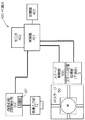
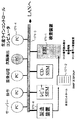
図15は、上記した検査システム1に適用可能な、本発明に係る欠陥検査装置の主要構成を示すブロック図である。該欠陥検査装置は、上記した検査アルゴリズム(セル検査法、隣接ダイ比較法、基準ダイ比較法、及びCADデータ比較法)を、予め設定したシーケンスに基づいて、選択的に実行できるよう構成されている。
図15において、5は干渉計からなるステージ位置取得部を示し、50は電子線装置を構成するXYステージを示し、500はステージ駆動部を示している。ステージ駆動部500は、図1及び図2に示したサーボモータ521、531及びエンコーダ522、532を含んでいる。また、図15において、72は電子光学系70を構成する画像入力部、
、300は画像処理/欠陥検出部、400はPC等のオペレータ用のコンピュータ端末(PC端末)である。
なお、本発明に係る欠陥検査装置においては、電子線装置として、SEM型及び写像投影型等の任意の電子線装置を採用可能であるが、欠陥検査装置として写像投影型の電子線装置を用いた場合、画像入力部72は、例えばCCDカメラからなるラインセンサである。Wは、ステージ50上に載置された半導体ウエハである。
FIG. 15 is a block diagram showing a main configuration of a defect inspection apparatus according to the present invention that can be applied to the
In FIG. 15, 5 indicates a stage position acquisition unit including an interferometer, 50 indicates an XY stage constituting the electron beam apparatus, and 500 indicates a stage driving unit. The
, 300 is an image processing / defect detection unit, and 400 is a computer terminal (PC terminal) for an operator such as a PC.
In the defect inspection apparatus according to the present invention, an arbitrary electron beam apparatus such as an SEM type or a mapping projection type can be adopted as the electron beam apparatus. However, a mapping projection type electron beam apparatus is used as the defect inspection apparatus. In such a case, the
図16は、ステージ50を移動させることにより、ウエハをどのように走査するかを説明するための模式図であり、図2における各矩形R0、R1、R2、…、RnのX軸方向幅は、ラインセンサ幅である1スワース(例えば、2048ドット)に等しい。
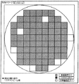
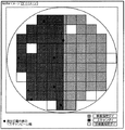
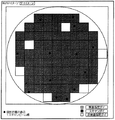
図17A〜Cは、PC端末400のモニタ402上に表示される画面の模式図であり、図17Aは検査開始時の画面、図17Bは検査中途の画面、図17Cは検査終了時の画面を表している。図17A〜C中、複数の正方形(長方形でもよい)はそれぞれ、ウエハ上のダイを表し、また、白抜きは、非検査指定ダイを示している。
FIG. 16 is a schematic diagram for explaining how the wafer is scanned by moving the
17A to 17C are schematic diagrams of screens displayed on the monitor 402 of the PC terminal 400. FIG. 17A is a screen at the start of the inspection, FIG. 17B is a screen during the inspection, and FIG. 17C is a screen at the end of the inspection. Represents. 17A to 17C, each of a plurality of squares (which may be rectangular) represents a die on the wafer, and white represents a non-inspection designated die.
図15、図16、図17A〜Cを参照して、本発明における欠陥検査装置の動作を説明する。
まず、オペレータが、PC端末400のモニタ402上で、検査レシピ(検査アルゴリズムを含む)、検査条件、検査ダイ指定、検査エリア指定、走査方向指定(双方向、順方向、又は逆方向)、ステージ速度指定等の、検査に必要な条件情報を初期設定する。以下においては、走査方向指定が双方向に設定されたものととして説明する。
The operation of the defect inspection apparatus according to the present invention will be described with reference to FIGS. 15, 16, and 17A to 17C.
First, an operator performs an inspection recipe (including an inspection algorithm), inspection conditions, inspection die specification, inspection area specification, scanning direction specification (bidirectional, forward direction, or reverse direction), stage on the monitor 402 of the PC terminal 400. Initialize condition information necessary for inspection such as speed designation. In the following description, it is assumed that the scanning direction designation is set to bidirectional.
初期設定が終了すると、PC端末400の制御部401は、モニタ402上に、図17Aに示すようなウエハの画面を表示させる。そして、欠陥検査がスタートすると、制御部401はステージ駆動部500を制御して、矩形R0のスタート位置Aの画像が画像入力部72から得られるよう、ステージ50の初期位置設定を行う。
次いで、制御部401は、ステージ駆動部500を制御して、ステージ50を−Y軸方向に移動させながら矩形R0の画像を取得し、ウエハW上の走査位置がストップ位置Bに到達して1走査が完了すると、Y軸方向の移動を停止させる。矩形R0の走査中、得られた画像データは、順次、画像処理/欠陥検出部300に送られて欠陥検出処理が実行され、その処理結果が欠陥検査結果記憶部301に記憶される。記憶部301は、少なくとも1つの矩形すなわち1走査分の欠陥検査結果データを格納可能な容量を有している。
When the initial setting is completed, the
Next, the
ウエハW上の走査がストップ位置Bに到達すると、制御部401は、ステージ駆動部500を制御して、ステージ50を−X軸方向に1スワース幅(例えば、2048ドットに相当する幅)ステップ移動させ、それに並行して、画像処理/欠陥検出部300に指示して、欠陥検査結果記憶部301から矩形R0の欠陥検査結果データを読み出させ、PC端末400の制御部401に転送させる。制御部401では、転送された欠陥検査結果データを欠陥検査結果記憶部403に格納する。この記憶部403は、全ての矩形R1〜Rnの欠陥検査結果データを記憶することができる容量を有している。
なお、画像処理/欠陥検出部300に記憶部301設けることなく、欠陥検査結果データを直接PC端末400に転送して、その記憶部403に格納しても良い。
そして、制御部401は、矩形R0の欠陥検査結果データを記憶部403から読み出し、未検査の矩形と識別可能とするために、色彩等を変えてモニタ402に表示させる。モニタ上402への表示は、ステージ位置取得部5からのX軸座標データに応じた位置に、1スワース幅の矩形で表示される。
When the scanning on the wafer W reaches the stop position B, the
Instead of providing the
Then, the
また、このとき、制御部401は、欠陥検査結果データが欠陥検出データを含んでいる場合には、その位置も色彩を変えて表示させる。欠陥の表示は、色彩を変える代わりに、形状を変化させても、また、○×等で表示しても良い。欠陥検出部300は、画像入力部(カメラ)72からの有効画素量(=画素数)で欠陥位置を管理する。制御部401は、スタート位置AのY軸座標を記憶しており、欠陥データを取得すると、スタート位置Aからそれまでの有効画素数に基づいて、モニタ402上の色彩を変化させる。例えば、1ピクセル100nmの倍率で観察している状態で、スタート時点から1スワース(=2048)×10の欠陥検査結果データを受け取ったときに、その時のデータが欠陥検出データである場合には、Y軸方向に10ピクセル分移動した位置が欠陥位置であることを表しているため、制御部401は、スタート位置Aから1000nmの位置の色彩を変化させる。
したがって、ステージ位置取得部5から、欠陥位置に対応するY軸座標を取得する必要がない。
At this time, if the defect inspection result data includes defect detection data, the
Therefore, it is not necessary to acquire the Y-axis coordinates corresponding to the defect position from the stage
X軸方向の1スワース幅のステップ移動が終了すると、制御部401は、ステージ駆動部500を制御して、ステージ50を+Y軸方向に移動させることにより、矩形R1のスタート位置Dからストップ位置Eまでの画像データが順次得られ、矩形R0の場合と同様に、画像処理/欠陥検出部300により欠陥検出が行われ、そして、ストップ位置Eに到達すると、矩形R1の欠陥検査結果データが制御部401に転送されかつモニタ402上に表示される。
Step movement of one swath width in the X axis direction is completed, the
このようにして、走査方向(Y軸方向)を反転しつつ矩形R0、R1、R2、…が順次検査され、かつPC端末400のモニタ402に図17Bに示すように表示される。オペレータがこのように表示された欠陥検査結果の画面を監視して、欠陥検出箇所が多数の場合又は欠陥検出箇所の面積の総和が大きい場合、ウエハW上の検査が完了していなくても、その時点でそのウエハの欠陥検査を終了させ、不良品であることを示すマークを当該ウエハに対応付けて、記憶部403に記憶させる。これにより、不良品を不要に検査する時間を短縮することができる。
最後の矩形Rnまで走査して欠陥検査処理を行った場合は、モニタ402に、図17Cに示すような画面が表示される。言うまでもなく、この時点であっても、オペレータは、不良品であるか否かを判定することができる。
In this way, the rectangles R 0 , R 1 , R 2 ,... Are sequentially inspected while reversing the scanning direction (Y-axis direction) and displayed on the monitor 402 of the PC terminal 400 as shown in FIG. The operator monitors the screen of the defect inspection result displayed in this way, and when the number of defect detection locations is large or the total area of the defect detection locations is large, even if the inspection on the wafer W is not completed, At that time, the defect inspection of the wafer is terminated, and a mark indicating a defective product is stored in the
When the defect inspection process is performed by scanning up to the last rectangle R n , a screen as shown in FIG. 17C is displayed on the monitor 402. Needless to say, even at this point, the operator can determine whether or not the product is defective.
なお、図8に関連して説明したように、欠陥検査を実行する前に、オペレータがウエハW上の非検査ダイ(検査除外ダイ)を指定することが好適である。上記したように、非検査ダイとして指定されたダイに対応する箇所は、図17A〜Cに示すように、色彩等を変えて他と識別してモニタ402上に表示される。非検査指定ダイには、例えば、ウエハ周辺の通常不良品であるダイ等の、予め不良品であることがわかっているダイが含まれる。
また、各ダイ中で所定の領域のみを検査するよう設定することもでき、その場合には、ダイ中の非検査領域に対応する箇所の色彩を変えて表示する。
As described with reference to FIG. 8, it is preferable that the operator designates a non-inspection die (inspection exclusion die) on the wafer W before executing the defect inspection. As described above, a location corresponding to a die designated as a non-inspection die is displayed on the monitor 402 while being distinguished from others by changing the color or the like, as shown in FIGS. Non-inspection designated dies include dies that are known to be defective in advance, such as dies that are normally defective around the wafer.
It is also possible to set to inspect only a predetermined area in each die, and in that case, the color corresponding to the non-inspection area in the die is changed and displayed.
上記においては、ステージ50のX軸方向へのステップ移動中に、すなわち、Y軸方向の1走査が終了する毎に、画像処理/欠陥検出部300から該1走査全体の欠陥検査結果データをPC端末400に転送してモニタ402上に表示できるようにしているが、1つの矩形Riの走査中であっても、1スワース(1検出単位)毎又は複数スワース毎の欠陥検査結果データが得られる毎に、該データを制御部401に転送して、逐次的にモニタ402上に表示するようにしてもよい。
この場合、ステージ位置取得部5から、現在の走査中のX軸座標及びY軸座標を取得し、その位置に、検出結果を表示すようにしてもよい。
In the above, during the step movement of the
In this case, the X-axis coordinate and the Y-axis coordinate during the current scanning may be acquired from the stage
また、上記したように、オペレータによるPC端末400上の設定により、ウエハWの走査方向を交互的に反転させて双方向走査を行う代わりに、順方向のみ又は逆方向のみの一方向走査を行ってもよい。いずれにしても、設定された走査の方向に応じて、制御部401がステージ駆動部500に指令して、ステージ50を駆動させることになる。
さらに、オペレータがPC端末400上で、良品として許容可能な欠陥位置の数又は面積の上限値(又は、上限値よりも低い警報値)を設定可能に構成することもできる。この場合、設定された上限値が記憶部403に記憶される。そして、制御部401は、欠陥検出部300から取得した欠陥検査結果データ中の欠陥位置又は面積を累算して、上限値に到達した時点でモニタ402上に不良品(又は、不良類似品)であることを表示させ、かつ、ステージ駆動部500の動作を停止させるようにする。
さらにまた、画像入力部72が2048ドットのラインセンサである場合、矩形RiとRi+1とが16ドット程度重なるように設定すると、ウエハ上のラインパターンの連続性判断等に好適である。
Further, as described above, instead of performing bidirectional scanning by alternately reversing the scanning direction of the wafer W according to the setting on the PC terminal 400 by the operator, unidirectional scanning is performed only in the forward direction or only in the reverse direction. May be. In any case, the
Further, the operator can set the upper limit value (or alarm value lower than the upper limit value) of the number or area of defect positions that are acceptable as non-defective items on the PC terminal 400. In this case, the set upper limit value is stored in the
Furthermore, when the
画像処理/欠陥検出部300における欠陥検出処理は、取得した画像データと参照画像データとを比較して、許容誤差以上の差分がある場合に欠陥と判定する、任意の手法を用いることができるが、上述したように、複数の検査アルゴリズムを選択的に実行可能に構成することが好ましい。
図18は、セル検査アルゴリズム及びダイ対ダイ検査アルゴリズム(隣接ダイ検査アルゴリズム)を選択的に実行可能な画像処理/欠陥検出部300の詳細な構成を示しており、302はセル参照画像生成部、303は画像比較部、304は欠陥判定部である。また、M1〜M3はそれぞれ画像メモリ、SW−A及びSW−Bは、PC端末400の制御部401からの制御信号によって切り替えられるスイッチである。
The defect detection processing in the image processing / defect detection unit 300 can use any method that compares the acquired image data with the reference image data and determines a defect when there is a difference greater than an allowable error. As described above, it is preferable that a plurality of inspection algorithms can be selectively executed.
FIG. 18 shows a detailed configuration of an image processing / defect detection unit 300 that can selectively execute a cell inspection algorithm and a die-to-die inspection algorithm (adjacent die inspection algorithm). 302 is a cell reference image generation unit, Reference numeral 303 denotes an image comparison unit, and 304 denotes a defect determination unit. M1 to M3 are image memories, and SW-A and SW-B are switches that are switched by a control signal from the
以下に、図18に示した画像処理/欠陥検出部300の動作を説明する。
オペレータがPC端末400上で、セル検査アルゴリズムを実行するように設定すると、制御部401は、欠陥検出部300のスイッチSW−Bを接点b3に接続する。セル検査アルゴリズムにおいては、画像メモリM1及びM2を使用しないので、スイッチSW−Aをどの接点に接続しても良い。
セル検査アルゴリズムにおいて、セル参照画像生成部302は、図13に関連して説明したように、セル検査の参照画像データを、検査対象であるセルの直前の複数のセルから検査と同時に取得するが、所定の周期で加重平均をとって生成するため、被検査領域の移動に伴って随時更新される。更新されたセル参照画像データは、随時、画像メモリM3に更新的に記憶される。
そして、画像比較部303が、その更新された参照画像データと現在取得された画像データ(画像入力部72から)とを比較してその差分を求め、欠陥判定部304が、得られた差分が所定の閾値よりも大きいか否かを判定し、大きい場合は、現在検査中の位置に欠陥が存在していると判定する。その結果は、記憶部301に記憶される。
The operation of the image processing / defect detection unit 300 shown in FIG. 18 will be described below.
When the operator sets on the PC terminal 400 to execute the cell inspection algorithm, the
In the cell inspection algorithm, the cell reference image generation unit 302 acquires the reference image data of the cell inspection from a plurality of cells immediately before the cell to be inspected at the same time as the inspection as described with reference to FIG. In order to generate a weighted average at a predetermined period, it is updated at any time as the region to be inspected moves. The updated cell reference image data is updated and stored in the image memory M3 as needed.
Then, the
オペレータによりダイ対ダイ検査アルゴリズムが設定された場合、制御部401は、奇数番目のダイの検査か偶数番目のダイの検査かに応じて、スイッチSW−Aを接点a1及びa2に交互接続するように切り替え、そして逆に、SW−Bを接点b2及びb1に交互に接続するように切り替える。どのダイであるかは、ステージ位置取得部5からの位置座標に基づいて判定することができる。
すなわち、検査中のダイが2n+1番目(奇数番目)である場合、スイッチSW−A及びSW−Bを接点a1及びb2に接続させ(又はその逆)、画像入力部72からのリアルタイムの画像データと、画像メモリM2に記憶された2n番目(偶数番目)のダイの画像データからなる参照画像データとが、画像比較部303に供給されるようにする。一方、検査中のダイが2n番目のダイである場合、スイッチSW−A及びSW−Bを接点a2及びb1に接続させ(又はその逆)、画像入力部72からのリアルタイムの画像データと、画像メモリM1に記憶された2n−1番目のダイの画像データからなる参照画像データとが、画像比較部303に供給されるようにする。
そして、セル検査アルゴリズムの場合と同様に、画像比較部303及び欠陥判定部304が、現在検査中の位置に欠陥があるか否かを判定し、その結果を欠陥検査結果記憶部301に記憶する。
When the die-to-die inspection algorithm is set by the operator, the
That is, when the die under inspection is the 2n + 1th (odd number), the switches SW-A and SW-B are connected to the contacts a1 and b2 (or vice versa), and the real-time image data from the
As in the case of the cell inspection algorithm, the
上記のアルゴリズムに加えて、欠陥検出部300を、基準ダイ比較検査アルゴリズム、及びCADデータ比較検査アルゴリズムの少なくとも一方も選択的に実行可能となるように構成し、それをPC端末400の制御部401で制御するようにしてもよい。また、各ダイについて、セル検査アルゴリズム及びダイ対ダイ検査アルゴリズムを、ダイ内の位置に応じて切り替えて実行しても良い。
また、上記したように、画像処理/欠陥検出部300に欠陥検査結果記憶部301を設けずに、欠陥判定部304の判定結果を直接、PC端末400に転送して欠陥検検査結果記憶部403に記憶させても良い。
In addition to the above algorithm, the defect detection unit 300 is configured so that at least one of the reference die comparison inspection algorithm and the CAD data comparison inspection algorithm can be selectively executed. You may make it control by. Further, for each die, the cell inspection algorithm and the die-to-die inspection algorithm may be switched and executed according to the position in the die.
Further, as described above, without providing the defect inspection
ところで、レシピの1つとして含まれるフォーカスマップレシピがあるが、該フォーカスマッピレシピの作成、及び該フォーカスマッピレシピにより実行される検査動作時のオートフォーカス動作について、図19〜図21を参照して説明する。
フォーカスマップレシピは、例えば、独立的な入力画面上で(又は、別の目的で設けられた入力画面上で)、オペレータによる次のステップにより作成される。
a)フォーカス値を入力するダイ位置やダイの中のパターン等、フォーカスマップ座標を入力する。(図19のスイッチ126・1)
b)フォーカス値を自動測定する場合に必要な、ダイパターンを設定する。このステップは、フォーカス値を自動測定しない場合、スキップできる。
c)上記a)で決められたフォーカスマップ座標のベストフォーカス値を設定する。
By the way, there is a focus map recipe included as one of the recipes. The creation of the focus map recipe and the autofocus operation during the inspection operation executed by the focus map recipe are described with reference to FIGS. explain.
The focus map recipe is created, for example, on the independent input screen (or on the input screen provided for another purpose) by the next step by the operator.
a) Input focus map coordinates such as a die position for inputting a focus value and a pattern in the die. (Switch 126.1 in FIG. 19)
b) A die pattern necessary for automatically measuring the focus value is set. This step can be skipped if the focus value is not automatically measured.
c) The best focus value of the focus map coordinates determined in the above a) is set.
この中で、a)のステップでは、オペレータが任意のダイを指定する事もできるが、全てのダイの選択や、n個毎のダイの選択などの設定も可能である。また入力画面はウエハ内のダイ配列を模式的に表現した図でも、実画像を使った画像でもオペレータが選択できる。
また、c)のステップでは、オペレータが、図18に示した画面上で、スイッチ126・3を選択して、マニュアルでフォーカス用電極の電圧値に連動したフォーカススイッチ126・2で設定するか、又は、スイッチ126・4を選択して、自動的にフォーカス値を求めるかにより、フォーカス値を設定することができる。
Among these, in step a), the operator can designate any die, but it is also possible to select all dies or select every n dies. The input screen can be selected by the operator, whether it is a diagram schematically representing the die arrangement on the wafer, or an image using an actual image.
In the step c), the operator selects the switch 126.3 on the screen shown in FIG. 18 and manually sets the switch with the focus switch 12.6 linked to the voltage value of the focus electrode. Alternatively, the focus value can be set by selecting the switch 126. 4 and automatically obtaining the focus value.
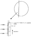
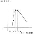
上記c)のステップで自動的にフォーカス値を求める手順は、コンピュータ演算により自動的に実行されるが、例えば、図20において、
a)フォーカス位置Z=1の画像を求めそのコントラストを計算し、
b)上記a)をZ=2,3,4でも行い、
c)上記a)、b)で得られたコントラスト値から回帰させコントラスト関数を求め(図20)、
d)コントラスト関数の最大値を得るZを計算で求め、これをベストフォーカス値とする
ことによって、得られる。
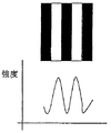
例えば、フォーカス値を自動測定する場合に必要なダイパターンが図21の様なライン&スペースである場合、良好な結果を示すが、コントラストは白黒パターンがあれば形状によらず計測できる。
上記のa)〜d)を行うことで、1点のベストフォーカス値Zが求まる。この時のデータ形式は(X,Y,Z)で表される。X及びYは、フォーカスを求めた座標、Zはベストフォーカス値である。したがって、フォーカスマップレシピで決められたフォーカスマップ座標値(X,Y,Z)が存在することになり、これをフォーカスマップレシピの一部でフォーカスマップファイルと呼ぶ。
The procedure for obtaining the focus value automatically in step c) is automatically executed by computer calculation. For example, in FIG.
a) Obtain an image at the focus position Z = 1, calculate its contrast,
b) The above a) is also performed with Z = 2, 3, 4;
c) A contrast function is obtained by regression from the contrast values obtained in the above a) and b) (FIG. 20),
d) It is obtained by calculating Z for obtaining the maximum value of the contrast function and setting it as the best focus value.
For example, when the die pattern necessary for automatically measuring the focus value is a line and space as shown in FIG. 21, good results are shown. However, if there is a monochrome pattern, the contrast can be measured regardless of the shape.
By performing the above a) to d), the best focus value Z of one point is obtained. The data format at this time is represented by (X, Y, Z). X and Y are coordinates for which focus is obtained, and Z is a best focus value. Therefore, focus map coordinate values (X, Y, Z) determined by the focus map recipe exist, and this is called a focus map file in a part of the focus map recipe.
このようにしてフォーカスマップレシピが作成されると、該フォーカスマップレシピに基づいて、以下のようにしてオートフォーカス動作が実行される。
a)フォーカスマップレシピの作成時に作成されたフォーカスマップファイル1を元に、位置情報をさらに細分化し、かつこの時のベストフォーカスを計算で求め、細分化したフォーカスマップファイル2を作成する。
b)上記a)の計算は、補間関数で行う。
c)上記b)の補間関数は、リニア補間やスプライン補間等でフォーカスマップレシピの作成時にオペレータにより指定される。
d)ステージの位置座標、すなわちTDIセンサの位置座標(Tx,Ty)を監視して、フォーカスマップファイル2に記述されている、現在のXY位置座表に適したフォーカス値に、フォーカス用電極の電圧を調整する。
さらに具体的に説明すると、図22において、黒丸がフォーカスマップファイル1のフォーカス値、白丸がフォーカスマップファイル2のフォーカス値であり、フォーカスマップファイル1のフォーカス値の間を、フォーカスマップファイル2のフォーカス値で補間している。そして、走査に従ってフォーカス位置Zを変化させるが、フォーカス値とフォーカス値との間は、次の変更する位置まで現在値が保持される。
When the focus map recipe is created in this way, the autofocus operation is executed as follows based on the focus map recipe.
a) Based on the
b) The calculation of a) is performed with an interpolation function.
c) The interpolation function of b) is specified by the operator when creating a focus map recipe by linear interpolation, spline interpolation, or the like.
d) The position coordinates of the stage, that is, the position coordinates (Tx, Ty) of the TDI sensor are monitored, and the focus value described in the
More specifically, in FIG. 22, the black circle is the focus value of the
図23は、図15に示した欠陥検査装置を使用した半導体製造プラントの例を示す。図23において、欠陥検査装置は参照番号171.1で示されており、該欠陥検査装置で検査されるウエハのロット番号、製造に経由した製造装置履歴等の情報は、SMIFまたはFOUP171・2に備えられたメモリから読み出されるか、または、そのロット番号を、SMIF、FOUP171・2又はウエハカセットのID番号を読み取ることにより、認識できるようになっている。ウエハの搬送中は、水分の量をコントロールしてメタル配線の酸化等を防止している。
欠陥検査装置171.1の欠陥検出制御用のPC171.6(すなわち、図15の制御部401)は、生産ラインの情報通信ネットワーク171・3に接続されており、このネットワーク171・3を介して、生産ラインを制御している生産ラインコントロールコンピュータ171・4、各製造装置171・5、及び別の検査システムに、被検査物であるウエハのロット番号などの情報とその検査結果を送ることができる。製造装置171・5には、リソグラフィー関連装置例えば露光装置、コーター、キュア装置、デベロッパ等、又は、エッチング装置、スパッタ装置及びCVD装置などの成膜装置、CMP装置、各種計測装置、他の検査装置、レビュー装置等が含まれる。
FIG. 23 shows an example of a semiconductor manufacturing plant using the defect inspection apparatus shown in FIG. In FIG. 23, the defect inspection apparatus is indicated by reference number 171.1. Information such as the lot number of the wafer to be inspected by the defect inspection apparatus and the history of the manufacturing apparatus that has been manufactured is stored in SMIF or FOUP 171-2. The lot number can be read out from the provided memory, or the lot number can be recognized by reading the SMIF, FOUP 171-2, or wafer cassette ID number. During the transfer of the wafer, the amount of moisture is controlled to prevent the metal wiring from being oxidized.
The PC 171.6 for defect detection control of the defect inspection apparatus 171.1 (that is, the
以上説明したように、本発明の欠陥検査装置によれば、半導体ウエハ等の欠陥検査を高スループットで行うことができ、もって、半導体ウエハの製造に大きく寄与することができる。 As described above, according to the defect inspection apparatus of the present invention, a defect inspection of a semiconductor wafer or the like can be performed with a high throughput, which can greatly contribute to the manufacture of a semiconductor wafer.
Claims (9)
試料上を走査することによって得られた試料表面の画像データと参照画像データとを対比して欠陥が存在するか否かを判定し、欠陥が存在するか否かを表す欠陥検査結果データを、走査に対応して出力する欠陥検出手段と、
欠陥検出手段からの欠陥検査結果データを受け取り、該データに基づいて、走査終了領域及び走査未終了領域を識別してモニタ上に表示させるよう制御する制御手段と
を備えていることを特徴とする欠陥検査装置。 In a defect inspection apparatus for inspecting a defect of a sample on which a pattern is formed,
By comparing the image data of the sample surface obtained by scanning the sample and the reference image data to determine whether or not a defect exists, defect inspection result data indicating whether or not a defect exists, Defect detection means for outputting corresponding to scanning;
Control means for receiving defect inspection result data from the defect detection means, and controlling to identify and display on the monitor a scanning end area and a scanning incomplete area based on the data. Defect inspection equipment.
該装置は、セル検査アルゴリズム及びダイ対ダイ検査アルゴリズムのいずれを実行すべきかの設定が可能であり、
制御手段は、セル検査アルゴリズム及びダイ対ダイ検査アルゴリズムのいずれが設定されたかに応じて、欠陥検出手段における基準画像データの取得及び格納を制御するよう構成されている
ことを特徴とする欠陥検査装置。 In the defect inspection apparatus in any one of Claims 1-5,
The apparatus can set whether to execute a cell inspection algorithm or a die-to-die inspection algorithm,
The control means is configured to control acquisition and storage of reference image data in the defect detection means in accordance with which one of the cell inspection algorithm and the die-to-die inspection algorithm is set. .
試料上に電子ビームを照射するための電子銃と、
電子銃からの電子ビームが試料上を走査するように、該電子ビームを偏向させる偏向器と、
電子ビームの試料上の走査により生成される、試料表面の情報を有する電子を検出して、試料表面の画像データを出力する検出器と
を備えていることを特徴とする欠陥検査装置。 The defect inspection apparatus according to any one of claims 1 to 6, wherein the apparatus further includes:
An electron gun for irradiating the sample with an electron beam;
A deflector for deflecting the electron beam so that the electron beam from the electron gun scans the sample;
A defect inspection apparatus comprising: a detector that detects electrons having information on a sample surface generated by scanning an electron beam on the sample and outputs image data of the sample surface.
試料上に電子ビームを照射するための電子銃と、
試料を保持するステージであって、電子銃からの電子ビームが試料上を走査するように移動可能な試料ステージと、
電子ビームの試料上の走査により生成される、試料表面の情報を有する電子を検出して、試料表面の画像データを出力する検出器と
を備えていることを特徴とする欠陥検査装置。 The defect inspection apparatus according to any one of claims 1 to 6, wherein the apparatus further includes:
An electron gun for irradiating the sample with an electron beam;
A stage for holding the sample, the sample stage being movable so that the electron beam from the electron gun scans on the sample; and
A defect inspection apparatus comprising: a detector that detects electrons having information on a sample surface generated by scanning an electron beam on the sample and outputs image data of the sample surface.
電子銃は、複数の画素を含むように、1又は複数本の電子ビームを試料上に照射するよう構成されており、
検出器は、試料表面の情報を有する電子に基づき、試料表面の画像を検出器上に結像するよう構成されている
ことを特徴とする欠陥検査装置。 The defect inspection apparatus according to claim 7 or 8,
The electron gun is configured to irradiate the sample with one or a plurality of electron beams so as to include a plurality of pixels,
The detector is configured to form an image of the sample surface on the detector based on electrons having information on the sample surface.
Priority Applications (3)
| Application Number | Priority Date | Filing Date | Title |
|---|---|---|---|
| JP2004105371A JP2005291833A (en) | 2004-03-31 | 2004-03-31 | Defect inspecting device of sample |
| US11/030,320 US20050205781A1 (en) | 2004-01-08 | 2005-01-07 | Defect inspection apparatus |
| US11/979,143 US20080063258A1 (en) | 2004-01-08 | 2007-10-31 | Defect inspection apparatus |
Applications Claiming Priority (1)
| Application Number | Priority Date | Filing Date | Title |
|---|---|---|---|
| JP2004105371A JP2005291833A (en) | 2004-03-31 | 2004-03-31 | Defect inspecting device of sample |
Publications (1)
| Publication Number | Publication Date |
|---|---|
| JP2005291833A true JP2005291833A (en) | 2005-10-20 |
Family
ID=35324934
Family Applications (1)
| Application Number | Title | Priority Date | Filing Date |
|---|---|---|---|
| JP2004105371A Pending JP2005291833A (en) | 2004-01-08 | 2004-03-31 | Defect inspecting device of sample |
Country Status (1)
| Country | Link |
|---|---|
| JP (1) | JP2005291833A (en) |
Cited By (11)
| Publication number | Priority date | Publication date | Assignee | Title |
|---|---|---|---|---|
| JP2007248360A (en) * | 2006-03-17 | 2007-09-27 | Jeol Ltd | Charged particle beam inspection method and apparatus |
| JP2007258064A (en) * | 2006-03-24 | 2007-10-04 | Topcon Corp | Inspection equipment |
| JP2008111770A (en) * | 2006-10-31 | 2008-05-15 | Makino Milling Mach Co Ltd | MEASUREMENT DISPLAY METHOD AND MECHANISM PROVIDED WITH MEASUREMENT DISPLAY DEVICE |
| JP2009168553A (en) * | 2008-01-15 | 2009-07-30 | Advanced Mask Inspection Technology Kk | Sample inspection apparatus and sample inspection method |
| JP2009283977A (en) * | 2009-08-21 | 2009-12-03 | Hitachi High-Technologies Corp | Inspection device and method |
| JP2010286500A (en) * | 2010-08-26 | 2010-12-24 | Advanced Mask Inspection Technology Kk | Sample inspection apparatus and sample inspection method |
| JP2011146607A (en) * | 2010-01-15 | 2011-07-28 | Djtech Co Ltd | Visual testing device |
| JP2012019220A (en) * | 2011-08-01 | 2012-01-26 | Hitachi High-Technologies Corp | Circuit pattern inspection device and circuit pattern inspection method |
| US8525984B2 (en) | 2007-03-28 | 2013-09-03 | Hitachi High-Technologies Corporation | Inspection apparatus and inspection method |
| CN114693668A (en) * | 2022-04-19 | 2022-07-01 | 苏州康钛检测科技有限公司 | Detection method of virtual interaction equipment wafer |
| CN115308231A (en) * | 2022-08-29 | 2022-11-08 | 广西岑科电子工业有限公司 | Automatic method and device for detecting defects of inductive magnetic core |
-
2004
- 2004-03-31 JP JP2004105371A patent/JP2005291833A/en active Pending
Cited By (11)
| Publication number | Priority date | Publication date | Assignee | Title |
|---|---|---|---|---|
| JP2007248360A (en) * | 2006-03-17 | 2007-09-27 | Jeol Ltd | Charged particle beam inspection method and apparatus |
| JP2007258064A (en) * | 2006-03-24 | 2007-10-04 | Topcon Corp | Inspection equipment |
| JP2008111770A (en) * | 2006-10-31 | 2008-05-15 | Makino Milling Mach Co Ltd | MEASUREMENT DISPLAY METHOD AND MECHANISM PROVIDED WITH MEASUREMENT DISPLAY DEVICE |
| US8525984B2 (en) | 2007-03-28 | 2013-09-03 | Hitachi High-Technologies Corporation | Inspection apparatus and inspection method |
| JP2009168553A (en) * | 2008-01-15 | 2009-07-30 | Advanced Mask Inspection Technology Kk | Sample inspection apparatus and sample inspection method |
| JP2009283977A (en) * | 2009-08-21 | 2009-12-03 | Hitachi High-Technologies Corp | Inspection device and method |
| JP2011146607A (en) * | 2010-01-15 | 2011-07-28 | Djtech Co Ltd | Visual testing device |
| JP2010286500A (en) * | 2010-08-26 | 2010-12-24 | Advanced Mask Inspection Technology Kk | Sample inspection apparatus and sample inspection method |
| JP2012019220A (en) * | 2011-08-01 | 2012-01-26 | Hitachi High-Technologies Corp | Circuit pattern inspection device and circuit pattern inspection method |
| CN114693668A (en) * | 2022-04-19 | 2022-07-01 | 苏州康钛检测科技有限公司 | Detection method of virtual interaction equipment wafer |
| CN115308231A (en) * | 2022-08-29 | 2022-11-08 | 广西岑科电子工业有限公司 | Automatic method and device for detecting defects of inductive magnetic core |
Similar Documents
| Publication | Publication Date | Title |
|---|---|---|
| US20080063258A1 (en) | Defect inspection apparatus | |
| JP4741408B2 (en) | XY coordinate correction apparatus and method in sample pattern inspection apparatus | |
| US7352195B2 (en) | Electron beam apparatus with detailed observation function and sample inspecting and observing method using electron beam apparatus | |
| US20050194535A1 (en) | Sample surface inspection method and inspection system | |
| US7408643B2 (en) | Method and apparatus for inspecting samples, and method for manufacturing devices using method and apparatus for inspecting samples | |
| US7928382B2 (en) | Detector and inspecting apparatus | |
| JP5066393B2 (en) | Foreign object / defect inspection / observation system | |
| JP6584946B2 (en) | Inspection device | |
| JP4642362B2 (en) | Substrate alignment method, substrate surface inspection method, substrate positioning method, semiconductor device manufacturing method, substrate alignment apparatus, and substrate surface inspection apparatus | |
| JP2005291833A (en) | Defect inspecting device of sample | |
| JP4279689B2 (en) | Electron beam equipment | |
| JP2005195504A (en) | Apparatus for inspecting defect in sample | |
| JP6737598B2 (en) | Inspection device and inspection method | |
| JP2006244875A (en) | Mapping projection type electron beam device and defect inspection system using the same | |
| JP2005091342A (en) | Sample defect inspection apparatus and method, and device manufacturing method using the defect inspection apparatus and method | |
| JP5302934B2 (en) | Sample surface inspection method and inspection apparatus | |
| JP4384022B2 (en) | Electron beam apparatus with detailed observation function, sample inspection using the electron beam apparatus, and sample observation method | |
| JP2004095281A (en) | Electron beam equipment | |
| JP2009135108A (en) | Mapping projection type electron beam apparatus and defect inspection system using the apparatus |