JP2005291758A - Test method and test program generating program of semiconductor integrated circuit - Google Patents
Test method and test program generating program of semiconductor integrated circuit Download PDFInfo
- Publication number
- JP2005291758A JP2005291758A JP2004103522A JP2004103522A JP2005291758A JP 2005291758 A JP2005291758 A JP 2005291758A JP 2004103522 A JP2004103522 A JP 2004103522A JP 2004103522 A JP2004103522 A JP 2004103522A JP 2005291758 A JP2005291758 A JP 2005291758A
- Authority
- JP
- Japan
- Prior art keywords
- test
- failure detection
- patterns
- detection rate
- program
- Prior art date
- Legal status (The legal status is an assumption and is not a legal conclusion. Google has not performed a legal analysis and makes no representation as to the accuracy of the status listed.)
- Withdrawn
Links
- 239000004065 semiconductor Substances 0.000 title claims abstract description 35
- 238000010998 test method Methods 0.000 title claims abstract description 21
- 238000012360 testing method Methods 0.000 claims abstract description 303
- 238000001514 detection method Methods 0.000 claims description 95
- 238000003860 storage Methods 0.000 claims description 14
- 238000000034 method Methods 0.000 claims description 11
- 238000004904 shortening Methods 0.000 abstract description 4
- 230000002950 deficient Effects 0.000 description 9
- 238000004806 packaging method and process Methods 0.000 description 4
- 238000004519 manufacturing process Methods 0.000 description 2
- 230000007423 decrease Effects 0.000 description 1
Images

Landscapes
- Tests Of Electronic Circuits (AREA)
- Testing Or Measuring Of Semiconductors Or The Like (AREA)
Abstract
Description
本発明は、半導体集積回路のテスト方法及び半導体集積回路のテストプログラム生成プログラムに関するものであり、より詳しくは、例えば、ウェハ試験やパッケージ試験等の複数の試験を行なう場合におけるテストプログラムの生成に関する。 The present invention relates to a test method for a semiconductor integrated circuit and a test program generation program for a semiconductor integrated circuit, and more particularly to generation of a test program when a plurality of tests such as a wafer test and a package test are performed.
従来より半導体集積回路に対しては、様々な試験(テスト)が行なわれている(例えば、特許文献1等)。半導体集積回路の試験には、ウェハ状態で行なわれるウェハ試験やパッケージ化後に行なわれるパッケージ試験がある。 Conventionally, various tests (tests) have been performed on semiconductor integrated circuits (for example, Patent Document 1). Semiconductor integrated circuit tests include a wafer test performed in a wafer state and a package test performed after packaging.
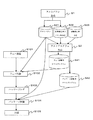
図4は、第1の従来例にかかるテスト方法を示すフローチャートである。このテスト方法では、まず、ウェハ試験とパッケージ試験の両方に適用する1つのテストパタンを生成する(S1)。1種類のテストパタンの生成には、例えば、コンピュータ2台で2日を要する。生成したテストパタンを記憶手段に格納する(S2)。そして、このテストパタンに基づき、テストプログラムを作成する(S3)。作成したテストプログラムに基づき、ウェハ試験用テストプログラム(S41)とパッケージ試験用のテストプログラム(S42)を作成する。 FIG. 4 is a flowchart showing a test method according to the first conventional example. In this test method, first, one test pattern to be applied to both the wafer test and the package test is generated (S1). For example, two computers need two days to generate one type of test pattern. The generated test pattern is stored in the storage means (S2). Based on this test pattern, a test program is created (S3). Based on the created test program, a wafer test test program (S41) and a package test program (S42) are created.
半導体ICは、図4に示されるように、ウェハ製造(S101)、ウェハ試験(S102)、パッケージング(S103)、パッケージ試験(S104)及び出荷(S105)の各工程を経て、製造、試験及び出荷が行なわれる。作成されたウェハ試験用テストプログラム(S41)に基づいてウェハ試験(S102)が実行され、良品/不良品の判定が行なわれる。また、パッケージ試験用のテストプログラム(S42)に基づいてパッケージ試験(S104)が実行され、良品/不良品の判定が行なわれる。 As shown in FIG. 4, the semiconductor IC is manufactured, tested, and processed through the steps of wafer manufacturing (S101), wafer test (S102), packaging (S103), package test (S104), and shipping (S105). Shipment is done. A wafer test (S102) is executed based on the created wafer test test program (S41), and a non-defective / defective product is determined. Further, the package test (S104) is executed based on the test program for package test (S42), and the non-defective / defective product is determined.
図5は、第2の従来例にかかるテスト方法を示すフローチャートである。このテスト方法では、まず、検出率の異なるウェハ試験用とパッケージ試験用の別々のテストパタンを生成する(S11、S12)。生成したテストパタンをそれぞれ記憶手段に格納する(S21、S22)。そして、ウェハ試験用テストパタンに基づいてウェハ試験用テストプログラムを作成し(S31)、記憶手段に格納する(S41)。また、パッケージ試験用テストパタンに基づいてパッケージ試験用テストプログラムを作成し(S32)、記憶手段に格納する(S42)。 FIG. 5 is a flowchart showing a test method according to the second conventional example. In this test method, first, separate test patterns for wafer test and package test having different detection rates are generated (S11, S12). The generated test patterns are stored in the storage means (S21, S22). Then, a wafer test test program is created based on the wafer test test pattern (S31) and stored in the storage means (S41). Further, a test program for package test is created based on the test pattern for package test (S32) and stored in the storage means (S42).
そして、作成されたウェハ試験用テストプログラム(S41)に基づいてウェハ試験(S102)が実行され、良品/不良品の判定が行なわれる。また、パッケージ試験用のテストプログラム(S42)に基づいてパッケージ試験(S104)が実行され、良品/不良品の判定が行なわれる。
上述の第1の従来例にかかるテスト方法によれば、ウェハ状態で行なわれるウェハ試験と、パッケージ化後のパッケージ試験とにおいて、同じテストパタンで実行するが、当該テストパタンは故障検出率を高くできるように作成された全部のテストパタンで実行されるため、ウェハ試験とパッケージ試験で同じテスト時間がかかり、テスト時間が長くなるという問題点があった。 According to the test method of the first conventional example described above, the wafer test performed in the wafer state and the package test after packaging are executed with the same test pattern, but the test pattern has a high failure detection rate. Since it is executed with all the test patterns created so that it can be performed, the same test time is required for the wafer test and the package test, and the test time becomes long.
上述の第2の従来例にかかるテスト方法によれば、テスト時間を短縮するために、ウェハ試験用とパッケージ試験用でテストパタンの異なる故障検出率のテストパタンを使用しようとすると、パッケージ試験用とウェハ試験用とで別々にテストパタンを作成する必要がある。そのため、テストパタン生成に余分な時間と、2つのテストパタンを記憶するハードウェアリソースが必要になる。この第2の従来例においては、パタン数と検出率対応情報がないため、テストパタンを生成した後では、走行パタン数を変更できないという問題点もある。 According to the test method according to the second conventional example described above, in order to shorten the test time, when trying to use test patterns having different failure detection rates for wafer test and package test, It is necessary to create test patterns separately for wafer test and wafer test. For this reason, extra time is required for test pattern generation and hardware resources for storing two test patterns are required. In the second conventional example, since there is no pattern number and detection rate correspondence information, there is also a problem that the travel pattern number cannot be changed after the test pattern is generated.
本発明は、かかる問題を解消するためになされたものであり、歩留りを殆ど変化させることなく、試験時間の短縮を図ることが可能な、半導体集積回路のテスト方法及びテストプログラム生成プログラムを提供することにある。 The present invention has been made to solve such a problem, and provides a test method and a test program generation program for a semiconductor integrated circuit capable of shortening a test time with almost no change in yield. There is.
本発明にかかるテスト方法は、半導体集積回路に対して少なくとも第1の試験と第2の試験を実行する半導体集積回路のテスト方法であって、作成された基準テストパタンの、前記半導体集積回路に対する故障検出率とテストパタン数の対応を求めるステップと、前記第1の試験に対する故障検出率を設定するステップと、前記設定された故障検出率に基づいて、前記故障検出率とテストパタン数の対応を参照して、当該故障検出率を達成するためのテストパタン数を算出するステップと、算出されたテストパタン数分の、前記基準テストパタンに含まれるテストパタンを第1の試験用テストパタンとして第1の試験用テストプログラムを作成するステップとを備えたものである。 A test method according to the present invention is a test method for a semiconductor integrated circuit that executes at least a first test and a second test on a semiconductor integrated circuit, and the reference test pattern thus created is applied to the semiconductor integrated circuit. Obtaining a correspondence between the failure detection rate and the number of test patterns; setting a failure detection rate for the first test; and correspondence between the failure detection rate and the number of test patterns based on the set failure detection rate The step of calculating the number of test patterns for achieving the failure detection rate, and the test pattern included in the reference test pattern for the calculated number of test patterns as a first test pattern for testing And creating a first test program for testing.
ここで、前記基準テストパタンを第2の試験用テストパタンとして第2の試験用テストプログラムを作成するステップを備えることが好ましい。 Here, it is preferable to include a step of creating a second test program using the reference test pattern as a second test pattern.
さらに、前記第2の試験に対する故障検出率を設定するステップと、前記設定された故障検出率に基づいて、前記故障検出率とテストパタン数の対応を参照して、当該第2の試験に対する故障検出率を達成するためのテストパタン数を算出するステップと、算出されたテストパタン数分の、前記基準テストパタンに含まれるテストパタンを第2の試験用テストパタンとして第2の試験用テストプログラムを作成するステップとを備えるようにしてもよい。 Further, a step of setting a failure detection rate for the second test and a failure for the second test with reference to the correspondence between the failure detection rate and the number of test patterns based on the set failure detection rate A step of calculating the number of test patterns for achieving the detection rate, and a test program for the second test, with the test patterns included in the reference test pattern as the second test pattern corresponding to the calculated number of test patterns May be provided.
前記故障検出率とテストパタン数の対応は、当該故障検出率とテストパタン数を対応付けたテーブルにより記憶手段に格納されることが望ましい。 The correspondence between the failure detection rate and the number of test patterns is preferably stored in the storage means by a table in which the failure detection rate and the number of test patterns are associated with each other.
また、前記第1の試験用テストプログラムにより、前記半導体集積回路に対して第1の試験を実行するステップと、前記第2の試験用テストプログラムにより、前記半導体集積回路に対して第2の試験を実行するステップとを備えるようにしてもよい。 A step of executing a first test on the semiconductor integrated circuit by the first test program for testing; and a second test on the semiconductor integrated circuit by the second test program for testing. May be provided.
好適な実施の形態において、前記第1の試験は、ウェハ試験であり、前記第2の試験はパッケージ試験である。 In a preferred embodiment, the first test is a wafer test, and the second test is a package test.
本発明にかかるテストプログラム生成プログラムは、半導体集積回路に対して第1の試験を実行するための第1の試験用テストプログラムと、第2の試験を実行するための第2の試験用テストプログラムを生成するためのテストプログラム生成プログラムであって、当該テストプログラム生成プログラムは、コンピュータに対して、基準テストパタンの、前記半導体集積回路に対する故障検出率とテストパタン数の対応を求めるステップと、前記第1の試験に対する故障検出率の設定するステップと、前記設定された故障検出率に基づいて、前記故障検出率とテストパタン数の対応を参照して、当該故障検出率を達成するためのテストパタン数を算出するステップと、算出されたテストパタン数分の、前記基準テストパタンに含まれるテストパタンを第1の試験用テストパタンとして第1の試験用テストプログラムを作成するステップとを実行させるものである。 A test program generation program according to the present invention includes a first test test program for executing a first test on a semiconductor integrated circuit, and a second test test program for executing a second test. A program for generating a test program, the test program generating program for obtaining a correspondence between a failure detection rate and a test pattern number of a reference test pattern for the semiconductor integrated circuit with respect to a computer; A step for setting a failure detection rate for the first test and a test for achieving the failure detection rate with reference to the correspondence between the failure detection rate and the number of test patterns based on the set failure detection rate A step of calculating the number of patterns, and tests included in the reference test pattern for the calculated number of test patterns Tan is intended to execute the steps of creating a first test for testing program as a first test test pattern.
ここで、前記基準テストパタンを第2の試験用テストパタンとして第2の試験用テストプログラムを作成するステップをさらにコンピュータに実行させることが好ましい。 Here, it is preferable that the computer further execute a step of creating a second test program using the reference test pattern as a second test pattern.
また、前記第2の試験に対する故障検出率を設定するステップと、前記設定された故障検出率に基づいて、前記故障検出率とテストパタン数の対応を参照して、当該第2の試験に対する故障検出率を達成するためのテストパタン数を算出するステップと、算出されたテストパタン数分の、前記基準テストパタンに含まれるテストパタンを第2の試験用テストパタンとして第2の試験用テストプログラムを作成するステップをさらにコンピュータに実行させるようにしてもよい。 A step of setting a failure detection rate for the second test, and referring to the correspondence between the failure detection rate and the number of test patterns based on the set failure detection rate, the failure for the second test A step of calculating the number of test patterns for achieving the detection rate, and a test program for the second test, with the test patterns included in the reference test pattern as the second test pattern corresponding to the calculated number of test patterns You may make it make a computer perform the step which produces this.
また、前記故障検出率とテストパタン数の対応は、当該故障検出率とテストパタン数を対応付けたテーブルにより記憶手段に格納されることが望ましい。 The correspondence between the failure detection rate and the number of test patterns is preferably stored in the storage means by a table in which the failure detection rate and the number of test patterns are associated with each other.
好適な実施の形態において、前記第1の試験は、ウェハ試験であり、前記第2の試験はパッケージ試験である。 In a preferred embodiment, the first test is a wafer test, and the second test is a package test.
本発明によれば、歩留りを殆ど変化させることなく、試験時間の短縮を図ることが可能な、半導体集積回路のテスト方法及びテストプログラム生成プログラムを提供することができる。 According to the present invention, it is possible to provide a test method for a semiconductor integrated circuit and a test program generation program capable of shortening a test time with almost no change in yield.
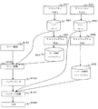
図1は、本発明にかかる半導体集積回路のテスト方法を示すフローチャートである。図に示されるように、半導体ICは、ウェハ製造(S101)、ウェハ試験(S102)、パッケージング(S103)、パッケージ試験(S104)及び出荷(S105)の各工程を経て、製造、試験及び出荷が行なわれる。当該ウェハ試験(S102)、パッケージ試験(S104)は、テストパタンに従う信号を入力端子に入力し、出力端子より出力される信号を検出する試験の他、いわゆるスキャンテストも含まれる。 FIG. 1 is a flowchart showing a method for testing a semiconductor integrated circuit according to the present invention. As shown in the figure, the semiconductor IC is manufactured, tested and shipped through the steps of wafer manufacture (S101), wafer test (S102), packaging (S103), package test (S104) and shipment (S105). Is done. The wafer test (S102) and package test (S104) include a so-called scan test in addition to a test in which a signal according to a test pattern is input to an input terminal and a signal output from the output terminal is detected.
本発明にかかる半導体集積回路のテスト方法においては、まず、基準となるテストパタン(以下、基準テストパタン)を作成する(S1)。基準テストパタンは、周知のテストパタン作成装置によって作成され、当該テストパタン作成装置の内部記憶手段又は外部記憶手段に格納される(S21)。作成されるテストパタン数は、試験対象となる半導体集積回路の構成によって大きく異なるが、例えば、500から数1000である。 In the method for testing a semiconductor integrated circuit according to the present invention, first, a reference test pattern (hereinafter referred to as a reference test pattern) is created (S1). The reference test pattern is created by a known test pattern creation device and stored in the internal storage means or the external storage means of the test pattern creation device (S21). The number of test patterns to be created varies greatly depending on the configuration of the semiconductor integrated circuit to be tested, but is, for example, 500 to several thousand.
基準テストパタンを作成する際に、同時に、故障検出率を算出し、当該故障検出率をパタン数と関連付けて記憶手段に格納しておく。この処理は、テストパタン作成装置によって実行することも可能であるが、テストパタン作成装置より基準テストパタンを出力し、出力された基準テストパタンに基づきテストプログラム作成装置により実行することも可能である。 At the time of creating the reference test pattern, at the same time, the failure detection rate is calculated, and the failure detection rate is associated with the number of patterns and stored in the storage means. This process can be executed by the test pattern creation device, but it is also possible to output a reference test pattern from the test pattern creation device and execute it by the test program creation device based on the outputted reference test pattern. .
テストプログラム作成装置は、例えば、テストプログラム生成プログラムをコンピュータにインストールすることにより構成される。当該コンピュータは、CPU、ROM、RAM、ハードディスク等のハードウェア構成を有するとともに、OS(Operation System)プログラム及びテストプログラム生成プログラム等のアプリケーションプログラムをハードディスク上に格納している。そして、適宜、これらのプログラムをRAM上に展開した上で、CPUにより所定の処理を実行する。 The test program creation device is configured, for example, by installing a test program generation program in a computer. The computer has a hardware configuration such as a CPU, ROM, RAM, and hard disk, and stores application programs such as an OS (Operation System) program and a test program generation program on the hard disk. Then, as appropriate, these programs are expanded on the RAM, and a predetermined process is executed by the CPU.
ここで、故障検出率について説明しておく。この故障検出率は、例えば、次の式によって算出する。
故障検出率=(S0+S1)/(S*2) ・・・ (1)
式(1)において、S0は所定のテストパタンで一度でも"0"になったノードの数、S1は所定のテストパタンで一度でも"1"になったノードの数、Sは全ノード数である。なお、ここで「ノード」とは、IC内部のそれぞれの信号線のことである。式(1)では故障モデルとして、縮退故障モデルを用いているため、テストパタンからより多くのノードが"0"及び"1"にセットされるパタンを検索すれば良い。この式は、全ノードの数の内のどれだけのノードが"0"及び"1"にセットされているか表したものなので、値が大きいと検出率が高いということになる。なお、縮退故障モデルは、単に一例にすぎないので、他の故障を検出したいならば、その故障モデルに見合った式を用いれば良い。
Here, the failure detection rate will be described. This failure detection rate is calculated by the following equation, for example.
Failure detection rate = (S0 + S1) / (S * 2) (1)
In Equation (1), S0 is the number of nodes that have become “0” even once with a predetermined test pattern, S1 is the number of nodes that have become “1” even once with a predetermined test pattern, and S is the total number of nodes. is there. Here, the “node” means each signal line inside the IC. Since the stuck-at fault model is used as the fault model in Equation (1), a pattern in which more nodes are set to “0” and “1” may be searched from the test pattern. Since this expression represents how many nodes among the total number of nodes are set to “0” and “1”, a larger value means a higher detection rate. Note that the stuck-at fault model is merely an example, and if it is desired to detect another fault, an equation corresponding to the fault model may be used.
故障検出率は、具体的には、試験対象となる半導体集積回路において論理演算により求めることが可能であり、コンピュータにより求めることが可能である。 Specifically, the failure detection rate can be obtained by a logical operation in a semiconductor integrated circuit to be tested, and can be obtained by a computer.
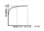
故障検出率とパタン数の対応を示すグラフを図2に示す。図に示されるように、故障検出率は、パタン数を増加させるに伴って増加する。しかしながら、パタン数の増加に伴う故障検出率の増加率は、パタン数の増加に伴って低下する。この例では、95%の故障検出率を得るためのパタン数は、98%の故障検出率を得るためのパタン数は約半分であり、後半の故障検出率の増加率は極めて低い。尚、パタン数の削減割合は回路の構成により異なる。 A graph showing the correspondence between the failure detection rate and the number of patterns is shown in FIG. As shown in the figure, the failure detection rate increases as the number of patterns increases. However, the increase rate of the failure detection rate accompanying the increase in the number of patterns decreases as the number of patterns increases. In this example, the number of patterns for obtaining a failure detection rate of 95% is about half that for obtaining a failure detection rate of 98%, and the rate of increase in the failure detection rate in the latter half is extremely low. Note that the reduction ratio of the number of patterns varies depending on the circuit configuration.
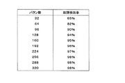
また、故障検出率とパタン数を関連付けることにより得られるテーブルの例を図3に示す。このテーブルは、図2に示すグラフの値を離散的な数値で表わしたものである。この例では、パタン数が256で故障検出率が98%に達し、その後320までパタン数を増加させても故障検出率は殆ど変化しない。他方、95%の故障検出率を得るためのパタン数は160であり、98%の故障検出率を得るためのパタン数256よりも極めて少ないことが判る。
An example of a table obtained by associating the failure detection rate with the number of patterns is shown in FIG. This table represents the values of the graph shown in FIG. 2 as discrete numerical values. In this example, when the number of patterns is 256 and the failure detection rate reaches 98%, the failure detection rate hardly changes even if the number of patterns is increased to 320 thereafter. On the other hand, the number of patterns for obtaining a failure detection rate of 95% is 160, which is found to be extremely smaller than the number of
また、ユーザは、テストプログラム作成装置に対してキーボード等の入力手段により故障検出率を入力して設定する。入力された故障検出率はテストプログラム作成装置における所定の記憶手段中に格納される。この故障検出率は、ウェハ試験、パッケージ試験のそれぞれにおいて、ユーザが必要と判断し、設定したものである。例えば、ウェハ試験を95%、パッケージ試験を98%と設定することができる。このとき、パッケージ試験の方が、ウェハ試験よりも後に実行されるため、より厳密なテストを行なう必要があるとの観点からすれば、ウェハ試験よりもパッケージ試験の方が故障検出率が高くなるように設定すべきである。他方、初期段階で厳しいテストを課す方が作業効率が高まるという観点に立てば、パッケージ試験よりもウェハ試験の方が故障検出率が高くなるように設定する。いずれにしても、本発明の実施の形態によれば、ウェハ試験とパッケージ試験とで、試験時間を短縮化するという観点から、異なる故障検出率を設定する必要がある。 In addition, the user inputs and sets the failure detection rate to the test program creation device using input means such as a keyboard. The inputted failure detection rate is stored in a predetermined storage means in the test program creation device. This failure detection rate is determined and set by the user as necessary in each of the wafer test and the package test. For example, the wafer test can be set to 95% and the package test can be set to 98%. At this time, since the package test is executed after the wafer test, the failure detection rate is higher in the package test than in the wafer test from the viewpoint that a stricter test is required. Should be set to On the other hand, from the viewpoint that working efficiency is higher when a severe test is imposed at the initial stage, the wafer test is set so that the failure detection rate is higher than the package test. In any case, according to the embodiment of the present invention, it is necessary to set different failure detection rates from the viewpoint of shortening the test time between the wafer test and the package test.
次に、基準テストパタン(S21)、故障検出率とパタン数を関連付けたテーブル(S22)、設定された故障検出率(S23)に基づいて、テストプログラムを生成する(S3)。 Next, a test program is generated based on the reference test pattern (S21), the table (S22) in which the failure detection rate and the number of patterns are associated, and the set failure detection rate (S23) (S3).
まず、ウェハ試験用テストプログラムの作成処理について説明する。ユーザは、テストプログラム作成装置に対してウェハ試験用テストプログラムの作成要求を入力する。この作成要求は、必ずしもユーザにより発生する必要はなく、テストプログラム作成装置内部において発生してもよい。テストプログラム作成装置は、インストールされたテストプログラム生成プログラムが起動することにより、当該作成要求に応じて、別途設定されたウェハ試験の故障検出率に基づいて故障検出率とパタン数を関連付けたテーブルを参照し、設定された故障検出率にするために必要なテストパタン数を算出する。図3に示す例において、設定されたウェハ試験の故障検出率が95%の場合には、パタン数160が算出される。尚、設定された故障検出率と同じ値が当該テーブル上にない場合には、当該テーブルにある値を内挿することにより対応するパタン数を算出してもよいし、設定された故障検出率よりも高い故障検出率で最も近い値の故障検出率をテーブル上で選択して、当該選択された故障検出率に対応するパタン数を抽出することによってパタン数を算出してもよい。
First, a process for creating a test program for wafer test will be described. The user inputs a request to create a test program for wafer test to the test program creation device. This creation request does not necessarily have to be generated by the user, and may be generated inside the test program creation apparatus. When the installed test program generation program is started, the test program creation device creates a table in which the failure detection rate and the number of patterns are associated with each other based on the failure detection rate of the wafer test set separately according to the creation request. Refer to and calculate the number of test patterns necessary to achieve the set failure detection rate. In the example shown in FIG. 3, when the failure detection rate of the set wafer test is 95%, the
テストプログラム作成装置は、このようにしてパタン数を算出すると、記憶手段に格納された基準テストパタンのうち、当該パタン数分のテストパタンをウェハ試験用のテストパタンとする。図3に示す例では、160のテストパタンがウェハ試験用のテストパタンとされ、ウェハ試験用テストプログラムが生成される(S41)。 When the number of patterns is calculated in this way, the test program creation device uses as many test patterns as the number of patterns among the reference test patterns stored in the storage means as test patterns for wafer testing. In the example shown in FIG. 3, 160 test patterns are used as wafer test patterns, and a wafer test test program is generated (S41).
次に、パッケージ試験用テストプログラムの作成処理について説明する。ユーザは、テストプログラム作成装置に対してパッケージ試験用テストプログラムの作成要求を入力する。この作成要求は、必ずしもユーザにより発生する必要はなく、テストプログラム作成装置内部において発生してもよい。テストプログラム作成装置は、インストールされたテストプログラム生成プログラムが起動することにより、当該作成要求に応じて、別途設定されたウェハ試験の故障検出率に基づいて故障検出率とパタン数を関連付けたテーブルを参照し、設定された故障検出率にするために必要なテストパタン数を算出する。図3に示す例において、設定されたパッケージ試験の故障検出率が98%の場合には、パタン数256が算出される。このとき、予めパッケージ試験の故障検出率として設定した値が、基準テストパタンを生成する際に設定された故障検出率の値と同じであれば、特にパタン数の算出を行なう必要がない。
Next, a process for creating a package test test program will be described. The user inputs a request to create a test program for package testing to the test program creation device. This creation request does not necessarily have to be generated by the user, and may be generated inside the test program creation apparatus. When the installed test program generation program is started, the test program creation device creates a table in which the failure detection rate and the number of patterns are associated with each other based on the failure detection rate of the wafer test set separately according to the creation request. Refer to and calculate the number of test patterns necessary to achieve the set failure detection rate. In the example shown in FIG. 3, when the failure detection rate of the set package test is 98%, the
テストプログラム作成装置は、このようにしてパタン数を算出すると、記憶手段に格納された基準テストパタンのうち、当該パタン数分のテストパタンをパッケージ試験用のテストパタンとする。図3に示す例では、256のテストパタンがパッケージ試験用のテストパタンとされ、パッケージ試験用テストプログラムが生成される(S42)。このとき、予めパッケージ試験の故障検出率として設定した値が、基準テストパタンを生成する際に設定された故障検出率の値と同じであれば、単純に、基準テストパタンの全パタンをパッケージ試験用テストパタンとしてパッケージ試験用テストプログラムを生成すればよい。 When the number of patterns is calculated in this way, the test program creation device uses as many test patterns as the number of patterns among the reference test patterns stored in the storage means as test patterns for package testing. In the example shown in FIG. 3, 256 test patterns are used as package test test patterns, and a package test test program is generated (S42). At this time, if the value set as the failure detection rate of the package test in advance is the same as the value of the failure detection rate set when generating the reference test pattern, all the patterns of the reference test pattern are simply packaged. A test program for package testing may be generated as a test pattern for testing.
作成されたウェハ試験用テストプログラムは、ウェハ試験(S102)において用いられ、同じく作成されたパッケージ試験用テストプログラムは、パッケージ試験(S104)において用いられる。 The created wafer test test program is used in the wafer test (S102), and the similarly created package test test program is used in the package test (S104).
このように、本発明にかかる半導体集積回路の試験方法によれば、テストプログラムを作成する際には、複数の試験のうち少なくとも一つの試験で用いられるテストパタン数について故障検出率とパタン数の対応から必要なパタン数を算出しているため、歩留りを殆ど低下させることなく、パタン数を削減することができ、試験時間を短縮化できる。 As described above, according to the method for testing a semiconductor integrated circuit according to the present invention, when creating a test program, the failure detection rate and the number of patterns for the number of test patterns used in at least one of a plurality of tests are determined. Since the required number of patterns is calculated from the correspondence, the number of patterns can be reduced without substantially reducing the yield, and the test time can be shortened.
また、ウェハ試験とパッケージ試験で故障検出率を変更することにより、一つテストパタンから、故障検出率の異なるテストプログラムを作成するようにしているため、テストパタンの生成は、一度のみでよい。従って、テストパタンの生成時間を短縮することができる。また、本発明によれば、テストパタン生成を2度行なわないため、テストパタン生成に要する時間、テストパタンを記憶するためのディスクのハードウェアリソースの削減が可能となる。 In addition, since the test programs having different failure detection rates are created from one test pattern by changing the failure detection rates in the wafer test and the package test, the test pattern may be generated only once. Therefore, the test pattern generation time can be shortened. Further, according to the present invention, since test pattern generation is not performed twice, it is possible to reduce the time required for test pattern generation and the hardware resources of the disk for storing the test pattern.
この例では、特にパッケージ試験においては、従来と同程度の故障検出率で試験を行なうため、不良品が最終的に顧客に流出することはない。 In this example, particularly in the package test, since the test is performed with the same failure detection rate as that in the past, the defective product does not eventually flow out to the customer.
尚、上述の例では、ウェハ試験とパッケージ試験を例示したが、これに限らず他の試験であってもよい。 In the above example, the wafer test and the package test are exemplified, but the present invention is not limited to this and may be other tests.
S1 テストパタン生成
S21 テストパタン
S22 故障検出率とパタン数対応
S23 故障検出率設定
S3 テストプログラム生成
S41 ウェハ試験用テストプログラム
S42 パッケージ試験用テストプログラム
S1 Test pattern generation S21 Test pattern S22 Failure detection rate and pattern number correspondence S23 Failure detection rate setting S3 Test program generation S41 Wafer test program S42 Package test program
Claims (11)
作成された基準テストパタンの、前記半導体集積回路に対する故障検出率とテストパタン数の対応を求めるステップと、
前記第1の試験に対する故障検出率を設定するステップと、
前記設定された故障検出率に基づいて、前記故障検出率とテストパタン数の対応を参照して、当該故障検出率を達成するためのテストパタン数を算出するステップと、
算出されたテストパタン数分の、前記基準テストパタンに含まれるテストパタンを第1の試験用テストパタンとして第1の試験用テストプログラムを作成するステップとを備えた半導体集積回路のテスト方法。 A method for testing a semiconductor integrated circuit, which performs at least a first test and a second test on a semiconductor integrated circuit,
Determining a correspondence between a failure detection rate and a test pattern number for the semiconductor integrated circuit of the created reference test pattern;
Setting a fault coverage for the first test;
Based on the set failure detection rate, referring to the correspondence between the failure detection rate and the number of test patterns, calculating the number of test patterns for achieving the failure detection rate;
A test method for a semiconductor integrated circuit, comprising: creating a first test test program by using, as the first test test pattern, the test patterns included in the reference test pattern for the calculated number of test patterns.
前記設定された故障検出率に基づいて、前記故障検出率とテストパタン数の対応を参照して、当該第2の試験に対する故障検出率を達成するためのテストパタン数を算出するステップと、
算出されたテストパタン数分の、前記基準テストパタンに含まれるテストパタンを第2の試験用テストパタンとして第2の試験用テストプログラムを作成するステップとをさらに備えたことを特徴とする請求項1記載の半導体集積回路のテスト方法。 Setting a fault coverage for the second test;
Calculating the number of test patterns for achieving the failure detection rate for the second test with reference to the correspondence between the failure detection rate and the number of test patterns based on the set failure detection rate;
The method further comprises the step of creating a second test program using the test patterns included in the reference test pattern as the second test pattern corresponding to the calculated number of test patterns. 2. A test method for a semiconductor integrated circuit according to 1;
前記第2の試験用テストプログラムにより、前記半導体集積回路に対して第2の試験を実行するステップとをさらに備えたことを特徴とする請求項1記載の半導体集積回路のテスト方法。 Executing a first test on the semiconductor integrated circuit by the first test program for testing;
2. The method for testing a semiconductor integrated circuit according to claim 1, further comprising a step of executing a second test on the semiconductor integrated circuit by the second test program for testing.
当該テストプログラム生成プログラムは、コンピュータに対して、
基準テストパタンの、前記半導体集積回路に対する故障検出率とテストパタン数の対応を求めるステップと、
前記第1の試験に対する故障検出率の設定するステップと、
前記設定された故障検出率に基づいて、前記故障検出率とテストパタン数の対応を参照して、当該故障検出率を達成するためのテストパタン数を算出するステップと、
算出されたテストパタン数分の、前記基準テストパタンに含まれるテストパタンを第1の試験用テストパタンとして第1の試験用テストプログラムを作成するステップとを実行させるテストプログラム生成プログラム。 A test program generation program for generating a first test test program for executing a first test on a semiconductor integrated circuit and a second test test program for executing a second test There,
The test program generation program is
Obtaining a correspondence between a failure detection rate of the reference test pattern and the number of test patterns for the semiconductor integrated circuit;
Setting a fault coverage for the first test;
Based on the set failure detection rate, referring to the correspondence between the failure detection rate and the number of test patterns, calculating the number of test patterns for achieving the failure detection rate;
A test program generation program that executes a step of creating a first test test program using the test patterns included in the reference test pattern as a first test pattern corresponding to the calculated number of test patterns.
前記設定された故障検出率に基づいて、前記故障検出率とテストパタン数の対応を参照して、当該第2の試験に対する故障検出率を達成するためのテストパタン数を算出するステップと、
算出されたテストパタン数分の、前記基準テストパタンに含まれるテストパタンを第2の試験用テストパタンとして第2の試験用テストプログラムを作成するステップをさらにコンピュータに実行させることを特徴とする請求項7記載のテストプログラム生成プログラム。 Setting a fault coverage for the second test;
Calculating the number of test patterns for achieving the failure detection rate for the second test with reference to the correspondence between the failure detection rate and the number of test patterns based on the set failure detection rate;
The computer is further caused to execute a step of creating a second test test program using the test patterns included in the reference test pattern as the second test pattern corresponding to the calculated number of test patterns. Item 8. A test program generation program according to Item 7.
8. The test program generation program according to claim 7, wherein the first test is a wafer test, and the second test is a package test.
Priority Applications (1)
| Application Number | Priority Date | Filing Date | Title |
|---|---|---|---|
| JP2004103522A JP2005291758A (en) | 2004-03-31 | 2004-03-31 | Test method and test program generating program of semiconductor integrated circuit |
Applications Claiming Priority (1)
| Application Number | Priority Date | Filing Date | Title |
|---|---|---|---|
| JP2004103522A JP2005291758A (en) | 2004-03-31 | 2004-03-31 | Test method and test program generating program of semiconductor integrated circuit |
Publications (1)
| Publication Number | Publication Date |
|---|---|
| JP2005291758A true JP2005291758A (en) | 2005-10-20 |
Family
ID=35324869
Family Applications (1)
| Application Number | Title | Priority Date | Filing Date |
|---|---|---|---|
| JP2004103522A Withdrawn JP2005291758A (en) | 2004-03-31 | 2004-03-31 | Test method and test program generating program of semiconductor integrated circuit |
Country Status (1)
| Country | Link |
|---|---|
| JP (1) | JP2005291758A (en) |
Cited By (1)
| Publication number | Priority date | Publication date | Assignee | Title |
|---|---|---|---|---|
| US9666304B2 (en) | 2014-04-02 | 2017-05-30 | Samsung Electronics Co., Ltd. | Method of testing semiconductor memory device, test device, and computer readable recording medium for recording test program for semiconductor memory device |
-
2004
- 2004-03-31 JP JP2004103522A patent/JP2005291758A/en not_active Withdrawn
Cited By (1)
| Publication number | Priority date | Publication date | Assignee | Title |
|---|---|---|---|---|
| US9666304B2 (en) | 2014-04-02 | 2017-05-30 | Samsung Electronics Co., Ltd. | Method of testing semiconductor memory device, test device, and computer readable recording medium for recording test program for semiconductor memory device |
Similar Documents
| Publication | Publication Date | Title |
|---|---|---|
| US20160378646A1 (en) | Method and system for generating functional test cases for software systems | |
| CN104950248B (en) | The circuit safety design for Measurability method and the detection method to hardware Trojan horse of accelerating hardware wooden horse triggering | |
| JP5762542B2 (en) | Computer-implemented method and persistent computer-readable medium for semiconductor process recipe verification | |
| US20060091928A1 (en) | Clock scaling circuit | |
| JP4908281B2 (en) | Power consumption analysis program, power consumption analysis method, and power consumption analysis apparatus | |
| CN110032505A (en) | Software quality determining device, software quality determine that method and software quality determine program | |
| US20110295536A1 (en) | Clock jitter analyzing method and apparatus | |
| JP2000235507A (en) | System reliability design apparatus and method, and recording medium recording system reliability design software | |
| JP4925200B2 (en) | Semiconductor wafer inspection equipment | |
| JP2005291758A (en) | Test method and test program generating program of semiconductor integrated circuit | |
| JP5179861B2 (en) | Semiconductor device | |
| JP4496006B2 (en) | Failure candidate identification system and failure candidate identification method | |
| CN120066511A (en) | Method, device, equipment and medium for generating data analysis and protocol analyzer | |
| JP6199813B2 (en) | Formal verification apparatus and program | |
| JP2014241066A (en) | Test method for integrated system | |
| JP4541196B2 (en) | Failure detection improvement device, failure detection improvement program, failure detection improvement method | |
| JP2011089833A (en) | Semiconductor device and method for generating test pattern of semiconductor device | |
| JP2011008620A (en) | Verification apparatus, verification method, and program | |
| JP3722690B2 (en) | Reliability verification device | |
| Heloue et al. | Efficient block-based parameterized timing analysis covering all potentially critical paths | |
| CN112433700B (en) | Development and operation method and device of robot application, electronic equipment and medium | |
| CN120447958B (en) | A logic checking method, device and computer equipment based on a low-code platform | |
| JP6658297B2 (en) | Test case generation method, test case generation program and test case generation device | |
| US9274172B2 (en) | Selective test pattern processor | |
| JP2012033091A (en) | Semiconductor circuit and test method for the same |
Legal Events
| Date | Code | Title | Description |
|---|---|---|---|
| A621 | Written request for application examination |
Free format text: JAPANESE INTERMEDIATE CODE: A621 Effective date: 20070110 |
|
| A761 | Written withdrawal of application |
Free format text: JAPANESE INTERMEDIATE CODE: A761 Effective date: 20070507 |