JP2005287275A - Power supply - Google Patents
Power supply Download PDFInfo
- Publication number
- JP2005287275A JP2005287275A JP2004102144A JP2004102144A JP2005287275A JP 2005287275 A JP2005287275 A JP 2005287275A JP 2004102144 A JP2004102144 A JP 2004102144A JP 2004102144 A JP2004102144 A JP 2004102144A JP 2005287275 A JP2005287275 A JP 2005287275A
- Authority
- JP
- Japan
- Prior art keywords
- converter
- voltage
- output
- power supply
- generator
- Prior art date
- Legal status (The legal status is an assumption and is not a legal conclusion. Google has not performed a legal analysis and makes no representation as to the accuracy of the status listed.)
- Pending
Links
Images


Classifications
-
- H—ELECTRICITY
- H02—GENERATION; CONVERSION OR DISTRIBUTION OF ELECTRIC POWER
- H02M—APPARATUS FOR CONVERSION BETWEEN AC AND AC, BETWEEN AC AND DC, OR BETWEEN DC AND DC, AND FOR USE WITH MAINS OR SIMILAR POWER SUPPLY SYSTEMS; CONVERSION OF DC OR AC INPUT POWER INTO SURGE OUTPUT POWER; CONTROL OR REGULATION THEREOF
- H02M1/00—Details of apparatus for conversion
- H02M1/36—Means for starting or stopping converters
-
- H—ELECTRICITY
- H02—GENERATION; CONVERSION OR DISTRIBUTION OF ELECTRIC POWER
- H02M—APPARATUS FOR CONVERSION BETWEEN AC AND AC, BETWEEN AC AND DC, OR BETWEEN DC AND DC, AND FOR USE WITH MAINS OR SIMILAR POWER SUPPLY SYSTEMS; CONVERSION OF DC OR AC INPUT POWER INTO SURGE OUTPUT POWER; CONTROL OR REGULATION THEREOF
- H02M3/00—Conversion of dc power input into dc power output
- H02M3/02—Conversion of dc power input into dc power output without intermediate conversion into ac
- H02M3/04—Conversion of dc power input into dc power output without intermediate conversion into ac by static converters
- H02M3/10—Conversion of dc power input into dc power output without intermediate conversion into ac by static converters using discharge tubes with control electrode or semiconductor devices with control electrode
- H02M3/145—Conversion of dc power input into dc power output without intermediate conversion into ac by static converters using discharge tubes with control electrode or semiconductor devices with control electrode using devices of a triode or transistor type requiring continuous application of a control signal
- H02M3/155—Conversion of dc power input into dc power output without intermediate conversion into ac by static converters using discharge tubes with control electrode or semiconductor devices with control electrode using devices of a triode or transistor type requiring continuous application of a control signal using semiconductor devices only
-
- H—ELECTRICITY
- H02—GENERATION; CONVERSION OR DISTRIBUTION OF ELECTRIC POWER
- H02M—APPARATUS FOR CONVERSION BETWEEN AC AND AC, BETWEEN AC AND DC, OR BETWEEN DC AND DC, AND FOR USE WITH MAINS OR SIMILAR POWER SUPPLY SYSTEMS; CONVERSION OF DC OR AC INPUT POWER INTO SURGE OUTPUT POWER; CONTROL OR REGULATION THEREOF
- H02M3/00—Conversion of dc power input into dc power output
- H02M3/22—Conversion of dc power input into dc power output with intermediate conversion into ac
- H02M3/24—Conversion of dc power input into dc power output with intermediate conversion into ac by static converters
- H02M3/28—Conversion of dc power input into dc power output with intermediate conversion into ac by static converters using discharge tubes with control electrode or semiconductor devices with control electrode to produce the intermediate ac
- H02M3/325—Conversion of dc power input into dc power output with intermediate conversion into ac by static converters using discharge tubes with control electrode or semiconductor devices with control electrode to produce the intermediate ac using devices of a triode or a transistor type requiring continuous application of a control signal
- H02M3/335—Conversion of dc power input into dc power output with intermediate conversion into ac by static converters using discharge tubes with control electrode or semiconductor devices with control electrode to produce the intermediate ac using devices of a triode or a transistor type requiring continuous application of a control signal using semiconductor devices only
- H02M3/338—Conversion of dc power input into dc power output with intermediate conversion into ac by static converters using discharge tubes with control electrode or semiconductor devices with control electrode to produce the intermediate ac using devices of a triode or a transistor type requiring continuous application of a control signal using semiconductor devices only in a self-oscillating arrangement
- H02M3/3385—Conversion of dc power input into dc power output with intermediate conversion into ac by static converters using discharge tubes with control electrode or semiconductor devices with control electrode to produce the intermediate ac using devices of a triode or a transistor type requiring continuous application of a control signal using semiconductor devices only in a self-oscillating arrangement with automatic control of output voltage or current
-
- H—ELECTRICITY
- H02—GENERATION; CONVERSION OR DISTRIBUTION OF ELECTRIC POWER
- H02M—APPARATUS FOR CONVERSION BETWEEN AC AND AC, BETWEEN AC AND DC, OR BETWEEN DC AND DC, AND FOR USE WITH MAINS OR SIMILAR POWER SUPPLY SYSTEMS; CONVERSION OF DC OR AC INPUT POWER INTO SURGE OUTPUT POWER; CONTROL OR REGULATION THEREOF
- H02M1/00—Details of apparatus for conversion
- H02M1/0067—Converter structures employing plural converter units, other than for parallel operation of the units on a single load
- H02M1/007—Plural converter units in cascade
Landscapes
- Engineering & Computer Science (AREA)
- Power Engineering (AREA)
- Dc-Dc Converters (AREA)
- Control Of Eletrric Generators (AREA)
Abstract
Description
本発明は、電源装置に関し、特に、発電機で得た電力から安定した電圧を取り出すことができる電源装置に関する。 The present invention relates to a power supply device, and more particularly to a power supply device that can extract a stable voltage from electric power obtained by a generator.
各種作業機を駆動する汎用エンジン等の制御装置用電源として、エンジン駆動される発電機の出力を利用したものが知られる。この種の電源装置では、エンジン回転数が低くて発電機からの入力電圧が低いときであっても、十分な電力を確保できることが要求される。しかし、低回転数で十分な電力を確保できるように設定すると、回転数が高くて発電機からの入力電圧が高いときには電力損失が大きくなるという問題がある。 As a power supply for a control device such as a general-purpose engine for driving various working machines, a power supply using an output of a generator driven by the engine is known. This type of power supply device is required to ensure sufficient power even when the engine speed is low and the input voltage from the generator is low. However, when setting is made so that sufficient power can be secured at a low rotational speed, there is a problem that power loss increases when the rotational speed is high and the input voltage from the generator is high.
この問題に対して、例えば、特開2002−51591号公報に記載されているように、発電機の出力を変圧器を介して制御装置の電源として供給するシステムが提案されている。このシステムによれば、変圧器で電圧が上昇するのを抑えて必要な電力を得ることができる。
エンジン発電機では、エンジンの回転数変動が大きいことがあり、上記公報に記載されたシステムのようにした場合、変圧器の入力電圧が数Vボルト(V)から500Vの範囲で変動することが予想される。したがって、高電圧を予定して変圧器を絶縁耐圧が大きいものにしたり、変圧器の出力側に設けられるダウンコンバータ等のスイッチング回路を高耐圧のものにしたりする必要がある。また、発電機出力は変圧器を介してダウンコンバータへ供給されるので、回転数が低い低電圧時には安定した電源確保が困難である。 In the engine generator, the engine speed fluctuation may be large, and when the system described in the above publication is used, the input voltage of the transformer may fluctuate in the range of several V volts (V) to 500V. is expected. Therefore, it is necessary to make the transformer have a high withstand voltage by planning a high voltage, or make the switching circuit such as a down converter provided on the output side of the transformer have a high withstand voltage. Further, since the generator output is supplied to the down converter via a transformer, it is difficult to secure a stable power source at a low voltage with a low rotation speed.
本発明の目的は、発電機出力の変動幅が大きい場合にも安定した出力電圧を確保することができる電源装置を提供することにある。 An object of the present invention is to provide a power supply apparatus capable of ensuring a stable output voltage even when the fluctuation range of the generator output is large.
上記目的を達成するための本発明は、交流発電機の出力を整流する整流回路と、該整流回路から出力された直流の降圧手段とを有する電源装置において、前記降圧手段が非絶縁型DC−DCコンバータであり、前記非絶縁型DC−DCコンバータの出力側に一次側が接続され、二次側を電源出力側とした自励発振型コンバータをさらに備えた点に第1の特徴がある。 In order to achieve the above object, the present invention provides a power supply apparatus having a rectifier circuit for rectifying the output of an AC generator and a DC step-down means output from the rectifier circuit, wherein the step-down means is a non-insulated DC- The DC converter is characterized in that it further includes a self-oscillation converter in which the primary side is connected to the output side of the non-insulated DC-DC converter and the secondary side is the power supply output side.
また、本発明は、前記非絶縁型DC−DCコンバータをデューティ制御するためのスイッチ手段と、前記交流発電機の交流出力電圧が予定値を超えるまでは前記スイッチ手段のオン状態を継続し、前記交流出力電圧が予定値を超えた時点で前記スイッチ手段のデューティ制御を開始するスイッチ手段駆動回路を備えた点に第2の特徴がある。 Further, the present invention provides a switch means for duty-controlling the non-insulated DC-DC converter, and continues the ON state of the switch means until the AC output voltage of the AC generator exceeds a predetermined value, A second feature is that a switch means driving circuit is provided which starts duty control of the switch means when the AC output voltage exceeds a predetermined value.
また、本発明は、前記自励発振型コンバータは、前記交流出力電圧が前記DC−DCコンバータでデューティ制御を開始する前記予定値に至るまでに動作を開始するように構成されている点に第3の特徴がある。 Further, the present invention is characterized in that the self-excited oscillation type converter is configured to start operation before the AC output voltage reaches the predetermined value at which duty control is started by the DC-DC converter. There are three features.
第1の特徴によれば、発電機出力は、まず非絶縁型DC−DCコンバータ回路で降圧され、この降圧された出力をさらに入力値として自励発振型コンバータで安定化した出力を形成するので、発電機出力の変動幅が大きい場合であっても安定した出力動作が可能な電源装置を提供することができる。 According to the first feature, the generator output is first stepped down by a non-insulated DC-DC converter circuit, and the stepped down output is further used as an input value to form a stabilized output by a self-excited oscillation type converter. In addition, it is possible to provide a power supply device capable of stable output operation even when the fluctuation range of the generator output is large.
また、自励発振型コンバータの前段に変圧器のない非絶縁型DC−DCコンバータを設けているので、変圧器を有する場合のように電圧の立ち上がり遅れや変圧器での損失がない。したがって、低回転時の発電出力を効率よく取り入れることができる。 In addition, since a non-insulated DC-DC converter without a transformer is provided in front of the self-excited oscillation converter, there is no voltage rise delay or loss at the transformer as in the case of having a transformer. Therefore, the power generation output at the time of low rotation can be taken in efficiently.
さらに、自励発振型コンバータは降圧された入力で動作するので、自励発振型コンバータの変圧器の耐圧を高く設定する必要がなく、電源装置全体の低コスト化を実現することができる。 Furthermore, since the self-excited oscillation type converter operates with a step-down input, it is not necessary to set the withstand voltage of the transformer of the self-excited oscillation type converter high, and the cost of the entire power supply device can be reduced.
第2の特徴によれば、低回転時には、非絶縁型DC−DCコンバータはオン状態に維持されるので発電機出力を全て電力源として活用することが可能である。一方、発電機出力が予定値以上に上昇した時点でデューティ制御を開始して自励発振型コンバータの入力電圧が抑制される。したがって、低回転時は無駄なく発電電力を効率的に利用しつつ、回転上昇後も抑制された入力電圧に基づいて安定した出力を得ることができる。 According to the 2nd characteristic, since a non-insulation type DC-DC converter is maintained in an ON state at the time of low rotation, it is possible to utilize all the generator outputs as a power source. On the other hand, duty control is started when the generator output rises above a predetermined value, and the input voltage of the self-excited oscillation converter is suppressed. Therefore, it is possible to obtain a stable output based on the input voltage that is suppressed even after the rotation is increased while efficiently using the generated power without waste during low rotation.
第3の特徴によれば、非絶縁型DC−DCコンバータの出力で動作する自励発振型コンバータでありながら、この自励発振型コンバータは非絶縁型DC−DCコンバータが、設定された最大電圧を出力するよりも以前に、つまり低い回転数域から素速く立ち上がって安定した電源を形成することができる。 According to the third feature, although the self-excited oscillation converter operates at the output of the non-isolated DC-DC converter, the non-isolated DC-DC converter has a set maximum voltage. It is possible to form a stable power supply by quickly starting up from a low rotational speed range before output of.
以下に図面を参照して本発明の一実施形態を詳細に説明する。図1は本発明の一実施形態に係る電源装置を含むエンジン発電装置の構成を示すブロック図である。エンジン発電装置としては、例えば、バッテリを備えていないか、バッテリを備えていてもバッテリが過放電であった場合等に手動で始動できるリコイルスタータを有するものが好適である。このエンジン発電機は、発電機1、整流回路2、DC−DCダウンコンバータ回路3、自励発振型コンバータ(RCC)4、およびECU5を有する。発電機1はエンジンで駆動されて、例えば定格運転状態において交流320Vの3相交流を出力する。この3相交流は整流回路2で整流されて、例えば直流450Vの電圧になって降圧型DC−DCコンバータ回路(以下、単に「ダウンコンバータ」という)3に入力される。ダウンコンバータ3は、入力された交流を半導体スイッチのスイッチングによるデューティ制御で所定の直流電圧、例えば40Vに降圧する。
Hereinafter, an embodiment of the present invention will be described in detail with reference to the drawings. FIG. 1 is a block diagram showing a configuration of an engine power generation device including a power supply device according to an embodiment of the present invention. As the engine power generation device, for example, a device having a recoil starter that can be started manually when the battery is not provided or the battery is overdischarged even if the battery is provided is suitable. The engine generator includes a
ダウンコンバータ3の出力側はRCC4の一次側に接続され、RCC4の二次側は発電機1を駆動するエンジンの制御装置つまりECU5に接続される。こうして、発電機1で発生した3相交流は、整流され、ダウンコンバータ3で例えば40Vに降圧され、さらにRCC4で例えば15Vの安定した電圧になって、ECU5に制御電源として供給される。
The output side of the
図2はダウンコンバータ3の基本回路構成を示す図である。このダウンコンバータ3はトランスを有しない非絶縁型である。図中、前記整流回路2の出力側(電圧Vin)のプラス側およびマイナス側間には、入力用コンデンサ6と、フライホイルダイオード7と、出力用コンデンサ8と、出力電圧検出用の抵抗9,10とが設けられる。
FIG. 2 is a diagram showing a basic circuit configuration of the
直流電源のマイナス側と出力用コンデンサ8のマイナス側との間に、Nチャネル型MOS−FET11とステップダウン用のチョークコイル(リアクトル)12とが直列接続される。FET11のゲートに電圧を印加するためにドライブ回路13が設けられる。ドライブ回路13は、FET11を導通・非導通(オン・オフ)するための駆動信号を出力する。ドライブ回路13から出力される駆動信号のデューティ(オン時間比)を決定するPWM信号(パルス信号)を形成するためのPWM回路14が設けられる。PWM回路14は、PWM信号のデューティを決定する基準電圧(三角波)Vrefを発生する発振回路(詳細は図3参照)23を有する。この基準電圧Vrefと抵抗9,10で分圧された電圧とを比較する比較器15が設けられる。
An N-channel MOS-
抵抗9,10で分圧された電圧が基準電圧Vrefより小さいとき、PWM回路14はFET11のオン状態を維持するため、100%のデューティでPWM信号を出力する。一方、抵抗9,10で分圧された電圧が基準電圧Vrefより大きいときには、PWM回路14は基準電圧Vrefと抵抗9,10の分圧とで決定される100%未満のデューティでPWM信号を出力する。
When the voltage divided by the
PWM回路14から出力されるPWM信号に従ってドライブ回路13はFET11のゲートに駆動信号を供給し、出力用コンデンサ8はFET11のオン時間比に応じた電圧で充電される。出力用コンデンサ8で平滑された平均充電電圧が出力電圧Voutである。出力電圧VoutはRCC4の一次側に接続される。
In accordance with the PWM signal output from the
図3は整流回路2およびダウンコンバータ3の回路図、図4はRCC4の具体的な回路図例を示しており、図1,図2と同符号は同一または同等部分を示す。図3において、整流回路2はダイオードブリッジ回路からなる。入力用コンデンサ6は整流回路2で整流された発電機1の出力を充電、平滑して入力直流電圧を形成する。ドライブ回路13は、フォトカプラ16とインバータバッファ17とインバータバッファ17の電源電圧を形成するツェナーダイオード18およびコンデンサ19を含む。インバータバッファ17に電源電圧が供給されると、インバータバッファ17の出力がFET11のゲートに供給されてFET11はオンになる。FET11のオン期間中のみ出力用コンデンサ8が充電される。
FIG. 3 is a circuit diagram of the rectifier circuit 2 and the
フォトカプラ16は、発光ダイオード20とフォトトランジスタ21を備えており、発光ダイオード20のカソードはPWM回路14の比較器15の出力側と接続されている。従って、PWM回路14からのPWM信号がオンの間、発光ダイオード20は駆動され、フォトトランジスタ21が導通してインバータバッファ17の入力が反転すると、FET11はオフになる。
The
フォトカプラ16の発光ダイオード20は、PWM回路14からのPWM信号によって付勢され、このPWM信号のデューティに基づいてフォトトランジスタ21のオン時間比、つまりFET11のデューティが決定される。
The
PWM回路14は、出力電圧Voutを代表する電圧(抵抗9,10による分圧)が、発振回路23で形成される基準電圧Vrefを超えた時に、100%未満のデューティでPWM信号を出力する。抵抗9,10による分圧は、出力電圧Voutが所定値(例えば40V)を越えたときに前記100%デューティのPWM信号を出力するように設定し、常に出力電圧が40Vに制限されるようにデューティ比が決定される。
The
図4において、RCC4は、一次側コイル24,25と二次側コイル26,27とからなるトランス28を有する。一次側コイル24,25は、FET29、トランジスタ30、およびフォトトランジスタ31を有する自励発振回路に接続される。フォトトランジスタ31は二次側のツェナーダイオード32および発光ダイオード33とともに、二次側を定電圧に制御するフィードバック回路を構成する。
In FIG. 4, the RCC 4 has a
RCC4の一次側に接続されるダウンコンバータ3の出力用コンデンサ8の充電電圧つまり出力電圧Voutは抵抗34a、34bおよび34cで分圧されてFET29のゲートに印加される。FET29がオンになると、コイル24に電流が流れてコイル25には巻線比に応じた電圧が発生する。コイル25で発生する電圧によってコンデンサ35の電圧が上昇し、トランジスタ30がオンになる。トランジスタ30がオンになることによってFET29はオフになる。
The charging voltage of the
FET29がオフになることにより、二次側のコイル26,27に、それぞれの巻線比に応じた電圧が発生し、出力用コンデンサ36,37が充電される。出力コンデンサ37の電圧が所定値(例えば15V)を超えると、発光ダイオード33が付勢されてフォトトランジスタ31がオンになる。そうすると、トランジスタ30がオンになってFET29のゲート電圧が低下し、FET29がオフになる。その結果、一次コイル24に電流が流れなくなり、二次側に発生する電圧が低下する。こうして、二次側コイル27の出力電圧が所定値つまり15Vに保持される。二次側コイル26からは、コイル27の出力電圧と異なる出力電圧(例えば17V)を得ることができる。
When the FET 29 is turned off, voltages corresponding to the respective winding ratios are generated in the secondary side coils 26 and 27, and the
二次側コイル26,27の出力電圧はエンジン発電機を始動・制御するための電源として利用される。 The output voltages of the secondary coils 26 and 27 are used as a power source for starting and controlling the engine generator.
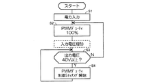
上記動作をフローチャートによって説明する。図5において、ステップS1で発電が開始されて電力が入力される。ステップS2では、PWM回路14のデューティを100%に設定する。なお、ここでいう100%とは、実質的にFET11をオン状態に維持するためのデューティをいい、例えば、デューティ95%程度も含むものとする。PWM回路14を100%デューティに設定することによってFET11が実質的にオンになると発電機の出力電圧の上昇に伴って出力電圧Voutが増大する。出力電圧が所定値(例えば40v)以上になるまではステップS2を維持し、出力電圧Voutが所定値以上になったならば、ステップS3が肯定になり、ステップS4に移行する。ステップS4では、PWM回路14がデューティ100%未満のPWM信号を出力し、ドライブ回路13はこのPWM信号に従ってFET11をスイッチングする。すなわち、出力電圧Voutが40Vに維持されるようにスイッチングのデューディ比を制御する。
The above operation will be described with reference to a flowchart. In FIG. 5, power generation is started in step S1 and electric power is input. In step S2, the duty of the
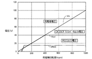
図6は、発電機1の回転数と電圧との関係を示す。図中、電圧Vinは発電機1の出力電圧を示し、電圧Voutはダウンコンバータ3の出力電圧を示し、電圧VRCCはRCC4の二次側コイル27の出力電圧を示す。図のように、発電機1の回転数の上昇に伴って電圧Vinは増大するが、電圧Voutは発電機1の回転数増大に拘わらず、所定値(例えば、40V)でデューティ制御により制限され、上昇が抑制される。また、電圧VRCCはRCC4の自励発振作用により、所定値(例えば、15V)で安定化される。
FIG. 6 shows the relationship between the rotational speed of the
電圧Voutが所定値つまり40Vに到達する以前にRCC4が動作を開始して電圧VRCCが所定値つまり15Vを発生するようにFET29のゲート電圧が設定される。図6に示すように、電圧VRCCは電圧Voutが40Vに到達する回転数以下の低い回転数域で15Vの安定した電圧を発生する。このように、自励発振型コンバータは、トランスによる昇圧機能を有しているので、この昇圧機能によって低回転数域で電圧Vinを超えた安定した出力電圧VRCCを得ることができる。 Before the voltage Vout reaches a predetermined value, that is, 40V, the RCC 4 starts to operate, and the gate voltage of the FET 29 is set so that the voltage VRCC generates a predetermined value, that is, 15V. As shown in FIG. 6, the voltage VRCC generates a stable voltage of 15 V in a low rotation speed region below the rotation speed at which the voltage Vout reaches 40 V. As described above, the self-excited oscillation type converter has a step-up function using a transformer, so that a stable output voltage VRCC exceeding the voltage Vin can be obtained in the low speed range by this step-up function.
本実施形態によれば、リコイルスタータでエンジンの始動操作を行った時等のように、低回転領域において発電機で誘起される低電圧によっても十分な出力電圧が得られ、ECUを立ち上げるための安定した電源を確保することができる。 According to this embodiment, a sufficient output voltage can be obtained even by a low voltage induced by a generator in a low rotation region, such as when an engine is started with a recoil starter, and the ECU is started up. Can ensure a stable power supply.
一方、エンジンが始動した後に回転数の上昇に伴って、発電機から高い出力電圧が発生した後もNチャネルFETの高速スイッチングにより出力電圧を制限することで小型の自励型発振コンバータで高効率運転を行うことができる。 On the other hand, even after a high output voltage is generated from the generator as the engine speed starts up, the output voltage is limited by high-speed switching of the N-channel FET. You can drive.
なお、本発明の制御電源は、エンジン発電機のECUの他、エンジンのチョーク開度制御用モータ、点火装置、バッテリ充電用、エンジンのスタータモータ用電源等、種々の電源装置として使用することができる。 The control power source of the present invention can be used as various power source devices such as an engine generator ECU, an engine choke opening control motor, an ignition device, a battery charging power source, and an engine starter motor power source. it can.
1…発電機、 3…ダウンコンバータ(非絶縁型DC−DCコンバータ)、 4…RCC(自励発振型コンバータ)、 8…出力用コンデンサ、 11…FET、 12…チョークコイル、 14…PWM回路、 15…比較器、 23…発振回路
DESCRIPTION OF
Claims (3)
前記降圧手段が非絶縁型DC−DCコンバータであり、
前記非絶縁型DC−DCコンバータの出力側に一次側が接続され、二次側を電源出力側とした自励発振型コンバータをさらに備えたことを特徴とする電源装置。 In a power supply device having a rectifier circuit for rectifying the output of an AC generator, and a step-down means for direct current output from the rectifier circuit,
The step-down means is a non-insulated DC-DC converter;
A power supply apparatus further comprising a self-excited oscillation type converter in which a primary side is connected to an output side of the non-insulated DC-DC converter and a secondary side is a power output side.
前記交流発電機の交流出力電圧が予定値を超えるまでは前記スイッチ手段のオン状態を継続し、前記交流出力電圧が予定値を超えた時点で前記スイッチ手段のデューティ制御を開始するスイッチ手段駆動回路を備えたことを特徴とする請求項1記載の電源装置。 Switch means for duty-controlling the non-insulated DC-DC converter;
The switch means driving circuit that continues the ON state of the switch means until the AC output voltage of the AC generator exceeds a predetermined value, and starts duty control of the switch means when the AC output voltage exceeds the predetermined value. The power supply device according to claim 1, further comprising:
Priority Applications (6)
| Application Number | Priority Date | Filing Date | Title |
|---|---|---|---|
| JP2004102144A JP2005287275A (en) | 2004-03-31 | 2004-03-31 | Power supply |
| CNB2005800091781A CN100452628C (en) | 2004-03-31 | 2005-03-15 | Power supply |
| PCT/JP2005/004518 WO2005099073A1 (en) | 2004-03-31 | 2005-03-15 | Power supply |
| US10/594,628 US7557547B2 (en) | 2004-03-31 | 2005-03-15 | Self exited oscillation converter providing a stable output voltage from a wide range of input voltages |
| EP05720775A EP1739816A4 (en) | 2004-03-31 | 2005-03-15 | Power supply |
| TW094109901A TWI351167B (en) | 2004-03-31 | 2005-03-30 | Power supply apparatus |
Applications Claiming Priority (1)
| Application Number | Priority Date | Filing Date | Title |
|---|---|---|---|
| JP2004102144A JP2005287275A (en) | 2004-03-31 | 2004-03-31 | Power supply |
Publications (1)
| Publication Number | Publication Date |
|---|---|
| JP2005287275A true JP2005287275A (en) | 2005-10-13 |
Family
ID=35125408
Family Applications (1)
| Application Number | Title | Priority Date | Filing Date |
|---|---|---|---|
| JP2004102144A Pending JP2005287275A (en) | 2004-03-31 | 2004-03-31 | Power supply |
Country Status (6)
| Country | Link |
|---|---|
| US (1) | US7557547B2 (en) |
| EP (1) | EP1739816A4 (en) |
| JP (1) | JP2005287275A (en) |
| CN (1) | CN100452628C (en) |
| TW (1) | TWI351167B (en) |
| WO (1) | WO2005099073A1 (en) |
Cited By (5)
| Publication number | Priority date | Publication date | Assignee | Title |
|---|---|---|---|---|
| JP2012186884A (en) * | 2011-03-03 | 2012-09-27 | Shindengen Electric Mfg Co Ltd | Power control circuit, power control device, and power control system |
| JP2012231557A (en) * | 2011-04-25 | 2012-11-22 | Mitsubishi Electric Corp | Power supply device |
| JP2015035908A (en) * | 2013-08-09 | 2015-02-19 | 三菱電機株式会社 | Step-down chopper circuit |
| CN107357348A (en) * | 2017-07-19 | 2017-11-17 | 中国科学院上海高等研究院 | A kind of AC signal amplitude accurate control circuit and method |
| CN107608443A (en) * | 2017-10-16 | 2018-01-19 | 中国科学院上海高等研究院 | A kind of AC signal amplitude accurate control circuit and method |
Families Citing this family (5)
| Publication number | Priority date | Publication date | Assignee | Title |
|---|---|---|---|---|
| US8890494B2 (en) | 2011-11-16 | 2014-11-18 | Rockwell Automation Technologies, Inc. | Wide input voltage range power supply circuit |
| US9252652B2 (en) | 2011-11-16 | 2016-02-02 | Rockwell Automation Technologies, Inc. | Wide input voltage range power supply circuit |
| US9155232B2 (en) | 2013-01-10 | 2015-10-06 | Rockwell Automation Technologies, Inc. | Wide input voltage range power supply circuit |
| US9755496B2 (en) | 2013-11-21 | 2017-09-05 | National Instruments Corporation | Solid state wideband high impedance voltage converter |
| DE102021100609A1 (en) * | 2021-01-14 | 2022-07-14 | Eberspächer Controls Landau Gmbh & Co. Kg | Starter system for an internal combustion engine in a vehicle |
Citations (4)
| Publication number | Priority date | Publication date | Assignee | Title |
|---|---|---|---|---|
| JPS61207168A (en) * | 1985-03-07 | 1986-09-13 | Seiko Epson Corp | Power source |
| JPS62221880A (en) * | 1986-03-19 | 1987-09-29 | Honda Motor Co Ltd | Portable engine power generator |
| JP2000217345A (en) * | 1999-01-20 | 2000-08-04 | Nec Corp | Boosting/dropping power source circuit |
| JP2002335670A (en) * | 2001-03-07 | 2002-11-22 | Matsushita Electric Ind Co Ltd | Dc-dc converter |
Family Cites Families (22)
| Publication number | Priority date | Publication date | Assignee | Title |
|---|---|---|---|---|
| US3353080A (en) * | 1964-08-06 | 1967-11-14 | Walden Electronics Corp | Regulated power supply having separate regulators responsive to different error signal frequency components |
| US3478256A (en) * | 1966-11-15 | 1969-11-11 | Yokogawa Electric Works Ltd | Capacitor potentiometer |
| US3967181A (en) * | 1970-05-06 | 1976-06-29 | Raytheon Company | Converter wherein switching frequency is independent of output voltage and is synchronized to an external system |
| US4030024A (en) * | 1976-07-02 | 1977-06-14 | Raytheon Company | Switching power supply with floating internal supply circuit |
| JPS591066B2 (en) * | 1978-12-27 | 1984-01-10 | 株式会社リコー | Constant voltage power supply startup method |
| FI66256C (en) * | 1981-01-26 | 1984-09-10 | Delcon Oy | ANALYSIS FOER FAELTSIGNALER I DATAMASKINER MICROPROCESSORSYSTEM ELLER DYLIKA DIGITAL ELECTRONIC SCREENS |
| GB8308100D0 (en) * | 1983-03-24 | 1983-05-05 | Rca Corp | Regulated power supply |
| US5239453A (en) * | 1990-12-21 | 1993-08-24 | Rolm Company | DC to DC converter employing a free-running single stage blocking oscillator |
| US5070439A (en) * | 1991-03-12 | 1991-12-03 | Rolm Corporation | DC to DC converter apparatus employing push-pull oscillators |
| US5430641A (en) * | 1992-04-27 | 1995-07-04 | Dell Usa, L.P. | Synchronously switching inverter and regulator |
| GB2275140B (en) * | 1993-02-13 | 1997-06-18 | Kijima Co Ltd | Push-pull inverter |
| JP3240020B2 (en) * | 1993-09-16 | 2001-12-17 | 本田技研工業株式会社 | Power supply for electric vehicles |
| JPH0898514A (en) * | 1994-09-16 | 1996-04-12 | Toko Inc | Switching power supply device |
| KR100268201B1 (en) * | 1993-11-12 | 2000-10-16 | 사까모또히로시 | Switching power supply device |
| JPH1023749A (en) * | 1996-07-03 | 1998-01-23 | Fuji Electric Co Ltd | Switching power unit |
| JP3224744B2 (en) * | 1996-07-08 | 2001-11-05 | 富士通株式会社 | Step-down DC-DC regulator |
| JP3527636B2 (en) * | 1998-06-12 | 2004-05-17 | 松下電工株式会社 | Self-excited DC-DC converter |
| DE10195883T1 (en) * | 2000-03-09 | 2003-05-08 | Ecoair Corp | Alternator system |
| US6707169B2 (en) * | 2000-07-19 | 2004-03-16 | Honda Giken Kogyo Kabushiki Kaisha | Engine generator, controller, starter apparatus, and remote control system for the engine generator |
| JP2002051591A (en) * | 2000-08-01 | 2002-02-15 | Honda Motor Co Ltd | Engine generator |
| JP4190795B2 (en) * | 2002-04-19 | 2008-12-03 | 日本電気通信システム株式会社 | Power circuit |
| JP4172203B2 (en) | 2002-05-10 | 2008-10-29 | トヨタ自動車株式会社 | Power supply system, power supply control method, and computer-readable recording medium storing a program for causing computer to execute power supply control |
-
2004
- 2004-03-31 JP JP2004102144A patent/JP2005287275A/en active Pending
-
2005
- 2005-03-15 WO PCT/JP2005/004518 patent/WO2005099073A1/en active Application Filing
- 2005-03-15 EP EP05720775A patent/EP1739816A4/en not_active Withdrawn
- 2005-03-15 US US10/594,628 patent/US7557547B2/en not_active Expired - Fee Related
- 2005-03-15 CN CNB2005800091781A patent/CN100452628C/en not_active Expired - Fee Related
- 2005-03-30 TW TW094109901A patent/TWI351167B/en not_active IP Right Cessation
Patent Citations (4)
| Publication number | Priority date | Publication date | Assignee | Title |
|---|---|---|---|---|
| JPS61207168A (en) * | 1985-03-07 | 1986-09-13 | Seiko Epson Corp | Power source |
| JPS62221880A (en) * | 1986-03-19 | 1987-09-29 | Honda Motor Co Ltd | Portable engine power generator |
| JP2000217345A (en) * | 1999-01-20 | 2000-08-04 | Nec Corp | Boosting/dropping power source circuit |
| JP2002335670A (en) * | 2001-03-07 | 2002-11-22 | Matsushita Electric Ind Co Ltd | Dc-dc converter |
Cited By (6)
| Publication number | Priority date | Publication date | Assignee | Title |
|---|---|---|---|---|
| JP2012186884A (en) * | 2011-03-03 | 2012-09-27 | Shindengen Electric Mfg Co Ltd | Power control circuit, power control device, and power control system |
| JP2012231557A (en) * | 2011-04-25 | 2012-11-22 | Mitsubishi Electric Corp | Power supply device |
| JP2015035908A (en) * | 2013-08-09 | 2015-02-19 | 三菱電機株式会社 | Step-down chopper circuit |
| CN107357348A (en) * | 2017-07-19 | 2017-11-17 | 中国科学院上海高等研究院 | A kind of AC signal amplitude accurate control circuit and method |
| CN107608443A (en) * | 2017-10-16 | 2018-01-19 | 中国科学院上海高等研究院 | A kind of AC signal amplitude accurate control circuit and method |
| CN107608443B (en) * | 2017-10-16 | 2019-03-12 | 中国科学院上海高等研究院 | A kind of AC signal amplitude accurate control circuit and method |
Also Published As
| Publication number | Publication date |
|---|---|
| US7557547B2 (en) | 2009-07-07 |
| CN1934773A (en) | 2007-03-21 |
| EP1739816A1 (en) | 2007-01-03 |
| WO2005099073A1 (en) | 2005-10-20 |
| EP1739816A4 (en) | 2010-05-05 |
| TWI351167B (en) | 2011-10-21 |
| CN100452628C (en) | 2009-01-14 |
| TW200539560A (en) | 2005-12-01 |
| US20070206394A1 (en) | 2007-09-06 |
Similar Documents
| Publication | Publication Date | Title |
|---|---|---|
| US10158282B1 (en) | Switching power supply device | |
| JP4013898B2 (en) | Power supply device startup method, power supply device startup circuit, and power supply device | |
| JP5268615B2 (en) | Power supply device and image forming apparatus | |
| US7557547B2 (en) | Self exited oscillation converter providing a stable output voltage from a wide range of input voltages | |
| JP4274364B2 (en) | DC-DC converter | |
| JP6071051B2 (en) | Switching power supply | |
| JP5387628B2 (en) | Current type isolated converter | |
| JP4632023B2 (en) | Power converter | |
| WO2016125561A1 (en) | Switching power supply device | |
| JP2006074965A (en) | Power supply device | |
| JP3236587B2 (en) | Switching power supply | |
| US7068020B2 (en) | Step-down DC—DC converter | |
| JP2017060271A (en) | Switching power supply device | |
| JP5408161B2 (en) | Self-excited switching power supply circuit | |
| JP4526879B2 (en) | DC power supply | |
| JP5901383B2 (en) | In-vehicle charging system | |
| US7729136B2 (en) | Isolated DC-DC converter | |
| JP4191874B2 (en) | Uninterruptible power system | |
| JP2022178982A (en) | Power supply circuit and power supply device | |
| JP2004328837A (en) | Switching power supply circuit and switching regulator comprising the same | |
| JP6053840B2 (en) | Power supply device and image forming apparatus | |
| JP2004328948A (en) | Switching power circuit and switching regulator equipped with the switching power circuit | |
| JP2005051942A (en) | Switching power circuit and switching regulator equipped with it | |
| JP2024014737A (en) | Switching power supply device, control method, and its integrated control circuit | |
| JP2000286080A (en) | High-pressure discharge lamp lighting device |
Legal Events
| Date | Code | Title | Description |
|---|---|---|---|
| A621 | Written request for application examination |
Free format text: JAPANESE INTERMEDIATE CODE: A621 Effective date: 20061130 |
|
| A131 | Notification of reasons for refusal |
Free format text: JAPANESE INTERMEDIATE CODE: A131 Effective date: 20091007 |
|
| A521 | Written amendment |
Free format text: JAPANESE INTERMEDIATE CODE: A523 Effective date: 20091105 |
|
| A131 | Notification of reasons for refusal |
Free format text: JAPANESE INTERMEDIATE CODE: A131 Effective date: 20100210 |
|
| A02 | Decision of refusal |
Free format text: JAPANESE INTERMEDIATE CODE: A02 Effective date: 20100623 |