JP2005267963A - Display device - Google Patents
Display device Download PDFInfo
- Publication number
- JP2005267963A JP2005267963A JP2004076519A JP2004076519A JP2005267963A JP 2005267963 A JP2005267963 A JP 2005267963A JP 2004076519 A JP2004076519 A JP 2004076519A JP 2004076519 A JP2004076519 A JP 2004076519A JP 2005267963 A JP2005267963 A JP 2005267963A
- Authority
- JP
- Japan
- Prior art keywords
- film
- phosphor
- display device
- picture element
- boron
- Prior art date
- Legal status (The legal status is an assumption and is not a legal conclusion. Google has not performed a legal analysis and makes no representation as to the accuracy of the status listed.)
- Pending
Links
Images


Classifications
-
- H—ELECTRICITY
- H01—ELECTRIC ELEMENTS
- H01J—ELECTRIC DISCHARGE TUBES OR DISCHARGE LAMPS
- H01J29/00—Details of cathode-ray tubes or of electron-beam tubes of the types covered by group H01J31/00
- H01J29/86—Vessels; Containers; Vacuum locks
- H01J29/88—Vessels; Containers; Vacuum locks provided with coatings on the walls thereof; Selection of materials for the coatings
-
- H—ELECTRICITY
- H01—ELECTRIC ELEMENTS
- H01J—ELECTRIC DISCHARGE TUBES OR DISCHARGE LAMPS
- H01J17/00—Gas-filled discharge tubes with solid cathode
- H01J17/02—Details
- H01J17/22—Means for obtaining or maintaining the desired pressure within the tube
- H01J17/24—Means for absorbing or adsorbing gas, e.g. by gettering
-
- H—ELECTRICITY
- H01—ELECTRIC ELEMENTS
- H01J—ELECTRIC DISCHARGE TUBES OR DISCHARGE LAMPS
- H01J2329/00—Electron emission display panels, e.g. field emission display panels
Abstract
Description
本発明は真空外囲器を備えた表示装置に係り、特に真空外囲器内のガス放出を抑制した表示装置に関するものである。 The present invention relates to a display device provided with a vacuum envelope, and more particularly to a display device that suppresses gas emission in a vacuum envelope.
表示装置としては、例えばテレビ受像管やディスプレイ管等の各種陰極線管、平面型表示装置としてプラズマディスプレイパネル、液晶表示装置、蛍光表示素子及び平行平板間に電界放出型電子源を備えた電界放出型表示装置(FED)等種々の型式のものが提案されている。 Examples of display devices include various cathode ray tubes such as television picture tubes and display tubes, and flat-panel display devices such as plasma display panels, liquid crystal display devices, fluorescent display elements, and field emission electron sources having a field emission electron source between parallel plates. Various types such as a display device (FED) have been proposed.
これらの表示装置のうち、真空外囲器を備えた表示装置としては前記陰極線管や蛍光表示素子、表面伝導型電子放出表示装置、電界放出型表示装置等が知られており、それぞれ優れた特徴を有している。 Among these display devices, the cathode ray tube, the fluorescent display element, the surface conduction electron emission display device, the field emission display device, and the like are known as display devices having a vacuum envelope, and each has excellent characteristics. have.
前記陰極線管はその精細な画像再現性を有していることから、各種の情報処理機器の表示手段として広く用いられている。 The cathode ray tube is widely used as a display means for various information processing devices because of its fine image reproducibility.
又、電界放出型表示装置のような平面型表示装置は、平行平板の構成で、前記陰極線管に比べ奥行寸法を格段に小さく出来、軽量化、薄型化が図れる等の特徴を備えている。 In addition, a flat display device such as a field emission display device has a parallel plate structure, and has features such that the depth dimension can be remarkably reduced compared to the cathode ray tube, and the weight and thickness can be reduced.
このような真空外囲器を備えた表示装置の中、前記陰極線管は、内面に蛍光体絵素とそれを取り囲む黒鉛を主体とするブラックマトリクス膜(以下BM膜と言う)及びこのBM膜と前記蛍光体絵素を覆う金属薄膜を有する蛍光面を備えたパネル部と、電子ビームを発生してこの電子ビームを蛍光面に向けて出射する複数の電極を有する電子銃を収容したネック部と、前記パネル部と前記ネック部とを連接して真空外囲器を構成するファンネル部とを備え、このファンネル部は内壁面に黒鉛を主成分とする内装導電膜を備えている。更に前記電子銃から発射される電子ビームを蛍光面上で走査させる偏向ヨークを外装した構成とされている。 In the display device having such a vacuum envelope, the cathode ray tube includes a black matrix film (hereinafter referred to as a BM film) mainly composed of a phosphor picture element and graphite surrounding the phosphor picture element, and a BM film. A panel portion having a phosphor screen having a metal thin film covering the phosphor picture element, and a neck portion containing an electron gun having a plurality of electrodes for generating an electron beam and emitting the electron beam toward the phosphor screen; The panel portion and the neck portion are connected to each other, and a funnel portion constituting a vacuum envelope is provided. The funnel portion includes an inner conductive film whose main component is graphite on the inner wall surface. Further, a deflection yoke for scanning an electron beam emitted from the electron gun on the phosphor screen is provided.
このような陰極線管において、前記内装導電膜は、蛍光面及び電子銃等に高電圧を印可する為の導電機能と、二次電子の吸収及び管内のガス吸着機能等を有しており、又この膜は黒鉛を主成分とし、これに膜の強度を高めると共にファンネルガラスとの密着性を高める機能をもつ珪酸カリウムと、膜の抵抗値を調整する目的の酸化チタン、その他の有機質等を含む構成となっている。 In such a cathode ray tube, the interior conductive film has a conductive function for applying a high voltage to a phosphor screen, an electron gun, etc., a secondary electron absorption function, a gas adsorption function in the tube, and the like. This film is mainly composed of graphite, and contains potassium silicate that has the function of increasing the strength of the film and improving the adhesion to the funnel glass, titanium oxide for adjusting the resistance of the film, and other organic substances. It has a configuration.
又、この種陰極線管の内装導電膜については、例えば下記特許文献1及び特許文献2などに開示されている。
The interior conductive film of this kind of cathode ray tube is disclosed in, for example, Patent Document 1 and
先ず、特許文献1には、ファンネル部内壁面に設けられた高抵抗黒鉛被膜と、この黒鉛被膜に接触して配置された高電圧導入部材と、前記黒鉛被膜の前記導入部材と接する近傍に前記黒鉛被膜よりも抵抗値の低い低抵抗黒鉛被膜を備え、前記高抵抗黒鉛被膜は酸化チタンと黒鉛と水ガラスとにより構成し、その比抵抗を1〜1000Ω・cmとし、
又前記低抵抗黒鉛被膜を酸化チタンと黒鉛と水ガラスもしくは黒鉛と水ガラスにより構成し、その比抵抗を0.001〜0.4Ω・cmとし、管内放電の防止と導通不良の発生
を皆無とすることが記載されている。
First, Patent Document 1 discloses a high-resistance graphite coating provided on the inner wall surface of a funnel, a high-voltage introducing member disposed in contact with the graphite coating, and the graphite coating in the vicinity of the graphite coating in contact with the introducing member. A low-resistance graphite film having a lower resistance value than the film, the high-resistance graphite film is composed of titanium oxide, graphite, and water glass, and the specific resistance is 1-1000 Ω · cm,
The low-resistance graphite coating is composed of titanium oxide and graphite and water glass or graphite and water glass, and the specific resistance is 0.001 to 0.4 Ω · cm, so that there is no prevention of discharge in the tube and the occurrence of poor conduction. It is described to do.
又、特許文献2には、ファンネル部内壁面に設けられた導電性被膜を黒鉛、水ガラス及び酸化チタンを主成分とする組成とし、酸化チタンの混合比を変えてアノードボタンと電子銃との中間部に位置する比抵抗が1〜10Ω・cmの高抵抗部、パネル部側に位置
する比抵抗が0.1Ω・cm以下の低抵抗部及びバルブスペーサコンタクトを有するネッ
ク部に位置する比抵抗が0.1〜1Ω・cmの中抵抗部となるように、スパーク電流値の
低減、耐削性、ガス吸着能等の機能に応じて設定して耐電圧特性及び寿命特性等の優れたソフトフッラシュ管を可能とすることが記載されている。
In
更に、特許文献2には、酸化鉄を用いない事からハロゲン対策が不要であることも記載されている。
Furthermore,
一方、平面型表示装置の一種である前記FEDでは特許文献3に開示されているように、真空外囲器は前面基板と背面基板及びこれら両基板間の周縁部に介挿された側壁(封止枠)とを封着して構成されており、このような真空外囲器内には、前記側壁で取り囲まれた領域内に前記両基板に作用する大気圧荷重を支持する複数の支持部材(スペーサ)が配置されている。又前記前面基板と背面基板間の間隔は数mm程度に設定されている。
On the other hand, in the FED, which is a kind of flat display device, as disclosed in
この真空外囲器内を高真空に維持するために、特許文献3では前記スペーサの高さを側壁の高さより低くし、側壁と両基板との封着の信頼性を確保して真空外囲器内を高真空に維持し、表示性能に優れた画像表示装置を提供することが記載されている。
このような構成からなる表示装置において、大型化、高性能化及び長寿命化の要求は厳しく、それに伴い真空外囲器内の高真空の維持が必至となっている。 In a display device having such a configuration, demands for larger size, higher performance, and longer life are severe, and accordingly, maintaining a high vacuum in the vacuum envelope is inevitable.
この真空外囲器内の高真空の維持には、排気作業時に完全な排気を行うことが最も重要であるが、動作中に管内に配置された電極類から残留ガスが発生することは避けられず、動作中のガス放出に伴う真空度劣化防止も不可欠な要因となっている。 In order to maintain a high vacuum in the vacuum envelope, it is most important to exhaust completely during the exhaust operation, but it is unavoidable that residual gas is generated from the electrodes arranged in the pipe during operation. In addition, prevention of deterioration of the degree of vacuum accompanying gas discharge during operation is also an indispensable factor.
表示装置の動作中に真空度が劣化すると、真空外囲器内の残留ガスの一部がイオン化してこれが電子放射面を衝撃し、これにより電子放射能力が阻害される恐れがある。 If the degree of vacuum is deteriorated during the operation of the display device, a part of the residual gas in the vacuum envelope is ionized and this impacts the electron emission surface, which may impair the electron emission capability.
管内残留ガスは、管内に配置された電極類、蛍光体、BM膜等多くの部材から発生することが知られており、特に陰極線管では管内の広範囲に亘って被着形成され、かつ構成材料の点も含めてファンネル部からネック部に亘って配置される内装導電膜からのガス放出量は多い。 It is known that the residual gas in the tube is generated from many members such as electrodes, phosphors, and BM films disposed in the tube. In particular, in a cathode ray tube, it is deposited over a wide area in the tube, and is a constituent material. Including this point, the amount of gas released from the interior conductive film disposed from the funnel portion to the neck portion is large.
この内装導電膜は、前記特許文献2にも開示された如く、管内残留ガスを吸着する機能も期待され、それらを含めて組成、粒径、膜抵抗値等について種々の検討がなさられているが、依然として放出量が吸着量を上回り、ガス放出を皆無とすることは困難であった。
As disclosed in
従って、管内残留ガスを軽減して長寿命化を得るために、管内に配置される例えば蛍光体絵素、BM膜及び内装導電膜等からのガス放出量を抑制することが解決すべき課題の一つとなっていた。 Therefore, in order to reduce the residual gas in the tube and obtain a long life, it is a problem to be solved to suppress the amount of gas released from, for example, the phosphor picture element, the BM film, the interior conductive film, and the like disposed in the tube. It was one.
本発明は、前述した従来の課題を解決するためになされたものであり、その目的は、蛍光体絵素、BM膜及び内装導電膜からの放出ガス量を抑制して長寿命の表示装置を提供することにある。 The present invention has been made to solve the above-described conventional problems, and an object of the present invention is to provide a long-life display device by suppressing the amount of gas released from the phosphor picture element, the BM film, and the inner conductive film. It is to provide.
このような目的を達成するために本発明による表示装置は、蛍光体絵素及びBM膜の少なくとも一方にホウ素を含む構成とした。 In order to achieve such an object, the display device according to the present invention is configured to include boron in at least one of the phosphor picture element and the BM film.
なお、本発明は、上記構成に限定されるものではなく、特許請求の範囲に記載した本発明の技術思想を逸脱しない範囲で種々の変更が可能であることは言うまでもない。 Needless to say, the present invention is not limited to the above-described configuration, and various modifications can be made without departing from the technical idea of the present invention described in the claims.
請求項1の発明によれば、蛍光体絵素及びBM膜の少なくとも一方からのガス放出を抑制出来るので、動作中の真空度劣化を防止でき、陰極の電子放射面の損傷を防止して高精細、長寿命の表示装置を提供することが出来る。 According to the first aspect of the present invention, gas emission from at least one of the phosphor picture element and the BM film can be suppressed, so that the degree of vacuum during operation can be prevented and damage to the electron emission surface of the cathode can be prevented. A display device with high definition and long life can be provided.
請求項2、3の発明によれば、陰極線管の蛍光体絵素、BM膜少なくとも1方及び内装導電膜からのガス放出を抑制出来るので、動作中の真空度劣化を防止でき、陰極の電子放射面の損傷を防止して高精細、長寿命の陰極線管を提供することが出来る。 According to the second and third aspects of the invention, gas emission from at least one of the phosphor picture element, the BM film, and the interior conductive film of the cathode ray tube can be suppressed, so that the degree of vacuum during operation can be prevented and the cathode electron It is possible to provide a high-definition and long-life cathode-ray tube by preventing the radiation surface from being damaged.
更に、内装導電膜からのガス放出を抑制出来るので、排気時間の短縮が可能となり、作業効率の向上と原価低減が可能となる。 Furthermore, since the gas emission from the interior conductive film can be suppressed, the exhaust time can be shortened, and the work efficiency can be improved and the cost can be reduced.
請求項4の発明によれば、平面型表示装置で前面基板の内表面の略全面に配置され、かつ最もガス放出源となる可能性の高い蛍光体絵素及びBM膜の少なくとも一方からのガス放出を抑制出来るので、動作中の真空度劣化を防止でき、陰極の電子放射面の損傷を防止して高精細、長寿命の平面型表示装置を提供することが出来る。 According to the fourth aspect of the present invention, the gas from at least one of the phosphor picture element and the BM film, which is arranged on substantially the entire inner surface of the front substrate and is most likely to be a gas emission source in the flat display device. Since emission can be suppressed, deterioration in vacuum during operation can be prevented, damage to the electron emission surface of the cathode can be prevented, and a flat display device with high definition and long life can be provided.
請求項5の発明によれば、蛍光体絵素、BM膜及び内装導電膜は一般に表面が多孔質であることから、例えばスプレー方式でホウ素の被着が可能で、作業性も優れている。
According to the invention of
請求項6の発明によれば、蛍光体絵素、BM膜及び内装導電膜製造用スラリーにホウ素を加えることで絵素、膜の製造と同時に形成することが可能となり、作業工程を短縮できる。
According to the invention of
又、絵素、膜全体にホウ素が混在するためガス放出抑制効果がより一層期待できる。 Further, since boron is mixed in the entire picture element and film, the effect of suppressing gas emission can be further expected.
本発明は、蛍光体絵素とこの蛍光体絵素を取り囲む黒鉛を主成分とするブッラクマトリクス膜とこのブッラクマトリクス膜と前記蛍光体絵素を覆う金属薄膜を有する蛍光面及びこの蛍光面に向けて電子を放出する電子源を真空外囲器内に備えた表示装置であって、前記蛍光体絵素及びブッラクマトリクス膜の少なくと一方ははホウ素を含むことを特徴としている。 The present invention relates to a phosphor screen having a phosphor matrix, a black matrix film mainly composed of graphite surrounding the phosphor picture element, a black matrix film and a metal thin film covering the phosphor picture element, and a phosphor screen. A display device having an electron source for emitting electrons in a vacuum envelope, wherein at least one of the phosphor picture element and the black matrix film contains boron.
以下、本発明の実施の形態について、実施例の図面を参照して詳細に説明する。 Embodiments of the present invention will be described below in detail with reference to the drawings of the embodiments.
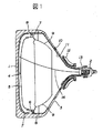
図1は、本発明による表示装置の一実施例を説明するシャドウマスク型カラー陰極線管の一例の概略構成を説明する模式断面図である。 FIG. 1 is a schematic cross-sectional view illustrating a schematic configuration of an example of a shadow mask type color cathode ray tube for explaining an embodiment of a display device according to the present invention.
同図において、1はパネル部で、このパネル部1はフラットパネル型と呼称され、フェース部が略フラット形状となっている。2はネック部、3はファンネル部で、このファンネル部3で前記パネル部1とネック部2とを連接してこれらで真空外囲器を構成している。4はパネル部1の内面に一般に赤(R)、緑(G)、青(B)の3色の蛍光体をモザイク状あるいはストライプ状に有する蛍光面、5は色選択電極としてのシャドウマスクで、このシャドウマスク5はプレス成形した自立形状保持型であり、その周辺をマスクフレーム6に溶接し、マスクフレーム6に固定した懸架スプリング7を介してパネル部1のスカート部内壁に植立したスタッドピン8に懸架支持される。なお、マスクフレーム6の電子銃側には外部磁界(地磁気)を遮蔽する磁気シールド9が取り付けられている。10は高圧導入端子で、この高圧導入端子10は前記ファンネル部3の略全内壁面からネック部2の一部に亘って被着形成された黒鉛を主成分とする内装導電膜11と接続している。この内装導電膜11の前記パネル部1側の端部は前記蛍光面4及びシャドウマスク5と電気的に接続されている。12は偏向ヨークで、この偏向ヨーク12は真空外囲器のネック−ファンネルの遷移領域に外装されている。13は3本の電子ビームを出射する電子銃で、この電子銃13の陽極には前記内装導電膜11を介して高電圧を印加している。14は3本の電子ビームのうちの1本を代表して示す電子ビームである。
In the figure, reference numeral 1 denotes a panel portion. The panel portion 1 is called a flat panel type, and the face portion has a substantially flat shape.
このような構成において、電子銃13から出射する3本の電子ビーム14は、図示しない外部信号処理回路から出力される映像信号により変調され、蛍光面4に向けて出射する。この出射された3本の変調された電子ビーム14を偏向ヨーク12で発生される水平と垂直との偏向磁界を通過させることにより、水平(X方向)と垂直(Y方向)に偏向して蛍光面4上を2次元走査させて画像を再現する。シャドウマスク5は、その面内に形成した多数の開孔で通過する3本の電子ビーム14のそれぞれを色毎に選択して所要の映像を再現する。
In such a configuration, the three
陰極線管は管内を排気した後に封止される。封止された直後の陰極線管は約10-3
〜10-4Paである。その後ゲッタフラッシュ、エージングを行うことで、約10-5〜10-6Pa迄真空度を向上させることができる。
The cathode ray tube is sealed after evacuating the inside of the tube. The cathode ray tube immediately after sealing is about 10 −3.
10 −4 Pa. Thereafter, the degree of vacuum can be improved to about 10 −5 to 10 −6 Pa by performing getter flash and aging.
図2は、図1に示したカラー陰極線管の蛍光面4の構成を説明する拡大した模式断面図である。
FIG. 2 is an enlarged schematic cross-sectional view for explaining the configuration of the
図2において、蛍光面4は赤色螢光体絵素41R、緑色螢光体絵素41G、青色螢光体絵素41Bの組み合わせからなる蛍光体絵素41と、黒鉛を主成分とし前記螢光体絵素41の周りを取り囲むBM膜42及びこのBM膜42と前記螢光体絵素41の電子銃13側を覆う金属薄膜43を有し、更に前記蛍光体絵素41とBM膜42はホウ素を含む構成となっている。このホウ素は蛍光体絵素41及びBM膜42を形成した後、水酸化ホウ素[B(OH)3]を純水で希釈した水溶液に蛍光体絵素41及びBM膜42を浸漬する方法等で含有させる。
In FIG. 2, the
又、前述ではホウ素を蛍光体絵素41及びBM膜42の両者に含ませる構成としたが、これは何れか一方、例えばBM膜42を形成した後、前述した水溶液にBM膜42を浸漬した後、螢光体絵素41を形成しても良い。更に蛍光体絵素41のみにホウ素を含ませる際には、例えば予め蛍光体スラリー中にホウ素を混入させる方法等で形成することが出来る。
In the above description, boron is included in both the
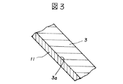
図3は、図1に示したカラー陰極線管のファンネル部3に被着形成された内装導電膜11の構成を説明する拡大断面図である。
FIG. 3 is an enlarged cross-sectional view for explaining the configuration of the interior
図3において、内装導電膜11はファンネル部3の内壁面3aに被着形成されており、この内装導電膜11は黒鉛を主成分としこれに膜の強度を高めると共にファンネルガラスとの密着性を高める機能をもつ珪酸カリウムと、膜の抵抗値を調整する機能を持つ酸化チタン、その他の有機質と、更にホウ素を含む構成となっている。
In FIG. 3, an interior
この実施例1に示す陰極線管では、蛍光体絵素とBM膜の少なくとも一方及び内装導電膜にホウ素を含む構成としたことにより、これら絵素、膜からのガス放出が抑制され、酸化性ガスの存在による陰極の劣化を防止でき、カラー陰極線管の長寿命化を可能にしている。 In the cathode ray tube shown in the first embodiment, since at least one of the phosphor picture element and the BM film and the interior conductive film contain boron, gas emission from these picture elements and film is suppressed, and the oxidizing gas Therefore, it is possible to prevent the cathode from being deteriorated due to the presence of the cathode and to extend the life of the color cathode ray tube.
又、実施例1では前述した構成により、ガス放出量が抑制されることから、陰極線管製造時の排気時間を短縮することが出来、これにより作業効率向上が図れ、それに伴う原価低減を可能にする特徴を有している。 Further, in the first embodiment, since the amount of gas emission is suppressed by the above-described configuration, the exhaust time at the time of manufacturing the cathode ray tube can be shortened, thereby improving the working efficiency and enabling the cost reduction associated therewith. It has the feature to do.
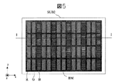
図4乃至図6は本発明の表示装置の他の実施例の電界放出型表示装置の一例の概略構 成を説明する図で、図4は模式展開斜視図、図5は図4の前面基板の背面基板側から 見た平面図、図6は図5のI−I線に沿った断面図である。 4 to 6 are diagrams for explaining the schematic configuration of an example of a field emission display device according to another embodiment of the display device of the present invention. FIG. 4 is a schematic exploded perspective view, and FIG. 5 is a front substrate of FIG. FIG. 6 is a cross-sectional view taken along the line II of FIG. 5.
図4乃至図6において、参照符号PN1は背面パネル、PN2は前面パネル、MFLは封止枠を示し、これら両パネルPN1、2と封止枠MFLを封着して真空外囲器を構成している。 4 to 6, reference numeral PN1 is a rear panel, PN2 is a front panel, MFL is a sealing frame, and both the panels PN1 and PN2 and the sealing frame MFL are sealed to form a vacuum envelope. ing.
背面パネルPN1を構成する背面基板SUB1の内面には多数の陰極配線が一方向(y方向)に延在しy方向に交差する他方向(x方向)に並設して形成され、この陰極配線に電気的に接続されて多数の電子源が配置されている。更にその上にx方向に延在しy方向に並設された多数のリボン状の金属薄板からなる制御電極MRGが設置されている。この各制御電極MRGには電子ビームを通過させる多数の貫通孔が設けられている。 On the inner surface of the back substrate SUB1 constituting the back panel PN1, a large number of cathode wirings are formed extending in one direction (y direction) and arranged in parallel in the other direction (x direction) intersecting the y direction. A number of electron sources are arranged in electrical connection. Furthermore, control electrodes MRG made of a number of ribbon-like thin metal plates extending in the x direction and arranged in parallel in the y direction are provided thereon. Each control electrode MRG is provided with a number of through holes through which an electron beam passes.
一方、前面パネルPN2を構成する前面基板SUB2の内面には蛍光体絵素R、G、BとBM膜BM及び金属薄膜からなる陽極(図示せず)を有し、背面パネルPN1に対して直角方向(z方向)に封止枠MLFを介して貼り合わされる。 On the other hand, the inner surface of the front substrate SUB2 constituting the front panel PN2 has phosphor picture elements R, G, B, a BM film BM, and an anode (not shown) made of a metal thin film, and is perpendicular to the rear panel PN1. Affixed in the direction (z direction) via the sealing frame MLF.
背面基板SUB1に形成される陰極配線と制御電極MRGの間には前記貫通孔部分を除いて絶縁層INSが介在されている。陰極配線から陰極配線引出端子CL−Tが引き出され、制御電極MRGから制御電極引出端子MRG−Tが引き出されている。また、背面パネルPN1と前面パネルPN2を貼り合わせた後、排気される。封止枠MFLで封止された内部は、例えば10-3〜10-5Paの真空に排気される。 An insulating layer INS is interposed between the cathode wiring formed on the back substrate SUB1 and the control electrode MRG except for the through hole portion. A cathode wiring lead terminal CL-T is drawn from the cathode wiring, and a control electrode lead terminal MRG-T is drawn from the control electrode MRG. Further, after the rear panel PN1 and the front panel PN2 are bonded together, the air is exhausted. The inside sealed with the sealing frame MFL is evacuated to a vacuum of 10 −3 to 10 −5 Pa, for example.
前面基板SUB2には蛍光体絵素R、G、Bが形成され、これらの蛍光体絵素の間には遮光性を持つBM膜BMが形成され、これら蛍光体絵素R,G,B及びBM膜BMはホウ素を含んだ構成となっている。このホウ素は蛍光体絵素R,G,B及びBM膜BMを形成した後、水酸化ホウ素[B(OH)3]を純水で希釈した水溶液に浸漬する方法等で含有される。更にこれら蛍光体絵素R,G,B及びBM膜BMは、その背面基板SUB1側を金属薄膜(図示せず)で覆っている。 Phosphor picture elements R, G and B are formed on the front substrate SUB2, and a light-shielding BM film BM is formed between the phosphor picture elements, and the phosphor picture elements R, G, B and The BM film BM includes boron. The boron is contained by, for example, a method of forming phosphor picture elements R, G, B and a BM film BM and then immersing it in an aqueous solution obtained by diluting boron hydroxide [B (OH) 3 ] with pure water. Further, these phosphor picture elements R, G, B and BM film BM cover the back substrate SUB1 side with a metal thin film (not shown).
蛍光体絵素は赤(R)、緑(G)、青(B)の配列で1画素を構成する。各色の間はBM膜BMで区画されている。このBM膜BMは黒色の導電体である。BM膜BMは色ずれの防止、コントラストの向上、蛍光膜のチャージアップ防止等に寄与している。 The phosphor picture element constitutes one pixel by arrangement of red (R), green (G), and blue (B). Each color is partitioned by the BM film BM. This BM film BM is a black conductor. The BM film BM contributes to prevention of color shift, improvement of contrast, prevention of charge-up of the fluorescent film, and the like.
このBM膜BMの抵抗値をコントロールする物質として、陰極線管等の表面処理に用いられている金属アルコキシド液を用いることができる。金属アルコキシド液の一例としてシリコンアルコキシド液がある。このシリコンアルコキシド液はテトラエトキシシランを溶媒であるエタノールに溶解してある。シリコンアルコキシド液に水と硝酸を加えると加水分解反応及び脱水縮合反応を起こし、ポリシロキサン結合を形成する。このポリシロキサン結合中に導電性粒子が取り込まれ安定した導電性を得ることができる。これにより、高圧が印加される前面パネルPN2の帯電対策が実現できる。このとき、BM膜の材料として、400°乃至450°で軟化する材料を用い、遮光性を付与するために酸化クロム(Cr2 O3 )、酸化鉄(Fe2 O3 )等の酸化物を添加すればよい。 As a substance for controlling the resistance value of the BM film BM, a metal alkoxide solution used for surface treatment of a cathode ray tube or the like can be used. An example of the metal alkoxide liquid is a silicon alkoxide liquid. This silicon alkoxide solution is obtained by dissolving tetraethoxysilane in ethanol as a solvent. When water and nitric acid are added to the silicon alkoxide solution, a hydrolysis reaction and a dehydration condensation reaction occur, and a polysiloxane bond is formed. Conductive particles are taken into this polysiloxane bond, and stable conductivity can be obtained. As a result, a countermeasure against charging of the front panel PN2 to which a high voltage is applied can be realized. At this time, a material that softens at 400 ° to 450 ° is used as the material of the BM film, and an oxide such as chromium oxide (Cr 2 O 3 ) or iron oxide (Fe 2 O 3 ) is used to impart light shielding properties. What is necessary is just to add.
BM膜に黒鉛を主成分とする前述の内装導電膜と同じ膜を適用することができる。 The same film as the above-described interior conductive film containing graphite as a main component can be applied to the BM film.
上記では蛍光体絵素R,G,B及びBM膜BMの両者共にホウ素を含んだ構成としたが、実施例1と同様に少なくとも一方でも良いことは勿論である。 In the above description, both the phosphor picture elements R, G, B and the BM film BM contain boron, but it is needless to say that at least one may be used as in the first embodiment.
この実施例2では、蛍光体絵素及びBM膜の少なくとも一方がホウ素を含む構成になっているため、パネル内のガス(酸化を促すガス)の量を抑制することができる。これにより陰極の劣化を防止でき、表示装置の長寿命化を図ることが出来る。 In Example 2, since at least one of the phosphor picture element and the BM film includes boron, the amount of gas (gas for promoting oxidation) in the panel can be suppressed. Thereby, the deterioration of the cathode can be prevented, and the life of the display device can be extended.
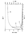
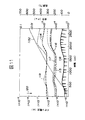
図7は本発明の表示装置を説明するための導電膜のガス放出量を昇温脱離法(TDS )で測定した結果を示す図である。 FIG. 7 is a graph showing the results of measuring the gas release amount of the conductive film by the temperature programmed desorption method (TDS) for explaining the display device of the present invention.
図7において、太実線111は本発明のガス放出量曲線を、又点線112は従来構造のガス放出量曲線を、更に実線113は温度曲線をそれぞれ示している。 In FIG. 7, a thick solid line 111 indicates a gas discharge amount curve of the present invention, a dotted line 112 indicates a gas discharge amount curve of a conventional structure, and a solid line 113 indicates a temperature curve.
図7においては、陰極線管製造工程における排気工程をシュミレートして測定したもので、試料は熱処理を施したガラス基板に、黒鉛と、珪酸カリウムと、酸化チタン及びその他の有機質を含む組成からなる導電膜を塗布し、乾燥後、この導電膜を純度6Nの水酸化ホウ素[B(OH)3]を100倍の純水で希釈した水溶液に浸漬、乾燥して形成した本発明のものと、前記導電膜を塗布し、乾燥しただけの従来構造のものとをそれぞれ準備し、比較評価した。 In FIG. 7, it is measured by simulating the exhaust process in the cathode ray tube manufacturing process. The sample is a conductive glass substrate that has been subjected to a heat treatment, made of a composition containing graphite, potassium silicate, titanium oxide, and other organic substances. After applying the film and drying, the conductive film was immersed in an aqueous solution of 6N pure boron hydroxide [B (OH) 3 ] diluted with 100 times pure water and dried, Each was prepared for comparison with a conventional structure having a conductive film applied and dried.
これらの試料を、実線1131で示す温度曲線に従って昇温して比較測定した結果、本発明のガス放出量は太実線1111で示すように約4分以内にガス放出が略無くなり、しかもガス放出量は1090Pa・L/g(パスカル・リットル/グラム)となった。
As a result of comparing and measuring these samples in accordance with the temperature curve shown by the
これに対し、点線1121で示す従来構造のものでは、本発明の略2倍の約8分間ガス放出が連続して確認され、又、ガス放出量も本発明の約3倍強の3600Pa・L/gとなっている。
On the other hand, in the case of the conventional structure indicated by the dotted
従って、本発明のものは従来構造に比べガス放出時間が半分以下に短縮され、しかもガス放出量も1/3以下に軽減することができた。 Therefore, according to the present invention, the gas release time was shortened to half or less as compared with the conventional structure, and the gas release amount could be reduced to 1/3 or less.
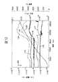
次に、図8は図7と同様に導電膜のガス放出量を昇温脱離法(TDS)で測定した結果を説明する図で、図8では陰極線管の動作時を想定したものである。 Next, FIG. 8 is a diagram for explaining the result of measuring the gas emission amount of the conductive film by the temperature programmed desorption method (TDS) as in FIG. 7, and FIG. 8 assumes the operation of the cathode ray tube. .
図8に示すガス放出特性は、図7で示すガス放出特性を測定した試料を真空中に放置して室温まで温度降下させ、これを再度実線1132で示す温度曲線に従って昇温して比較測定した結果を示したものである。なお、昇温速度は13℃/分とした。
The gas release characteristics shown in FIG. 8 were comparatively measured by allowing the sample for which the gas release characteristics shown in FIG. 7 were measured to stand in a vacuum and allowing the temperature to drop to room temperature, raising the temperature again according to the temperature curve shown by the
図8において、太実線1112で示す本発明のものでは、動作開始後約400℃でガス放出が始まり、略500℃でピークとなるがその値は極めて小さく、ガス放出量は約180Pa・L/gとなった。
In FIG. 8, in the thing of this invention shown by the thick
一方、従来構造のものでは、点線1122で示すように400℃近辺でガス放出が始まり略500℃で最大値となり、この間約100℃の温度上昇時間内に極めて急峻にガス放出が増加し続ける。その後500℃を超えると減少傾向となるが、更に550℃付近に第2のピークを有し、ガス放出量は本発明の約4倍の約760Pa・L/gとなり、管球動作時においてはその差が更に顕著となることを教示している。
On the other hand, in the case of the conventional structure, as shown by a dotted
この図7、図8に示す効果は、蛍光体絵素に付いても略同様であったが、蛍光体絵素では更に輝度向上効果も見られた。 The effects shown in FIGS. 7 and 8 were substantially the same when applied to the phosphor picture element. However, the luminance improvement effect was further observed with the phosphor picture element.
次に図9乃至図12は、導電膜から放出されるガス成分を示す図で、図9は図7の太実線1111のケースを、図10は図7の点線1121のケースを、又図11は図8の太実線1112のケースを、更に図12は図8の点線1122のケースをそれぞれ示している。
Next, FIGS. 9 to 12 are diagrams showing gas components released from the conductive film. FIG. 9 shows the case of the thick solid line 1111 in FIG. 7, FIG. 10 shows the case of the dotted
図9乃至図12において、太点線114はH2O成分を、細点線115はCO2成分を、太一点鎖線116は(N2+CO)成分を、細実線117はH2成分を、太実線118はO2成分をそれぞれ示し、更に細一点鎖線119は全圧を、又矢印120はバックグランド値を示している。バックグランド値は、加熱前に既に管内に存在するガス成分量の値である。
9 to 12, the thick dotted
これら図9乃至図12から明らかなように、本発明は、細点線115で示すCO2成分及び太一点鎖線116で示す(N2+CO)成分の二成分で従来構造との差が大きく、これがガス放出量抑制の要因となっていると思われる。
As is apparent from FIGS. 9 to 12, the present invention has two components, ie, a CO 2 component indicated by a thin
又、前述の実施例1、2では蛍光体絵素、BM膜及び内装導電膜をホウ素の水溶液に浸漬してホウ素含有としたが、浸漬に代えて前記水溶液をスプレーにより吹き付け塗布した別の実施例の試料においてもガス放出抑制効果は略同一であった。 In Examples 1 and 2, the phosphor picture element, the BM film, and the interior conductive film were immersed in an aqueous solution of boron to contain boron. However, instead of the immersion, the aqueous solution was sprayed and applied by spraying. Also in the sample of the example, the gas emission suppressing effect was substantially the same.
これは前述したように、蛍光体絵素、BM膜及び内装導電膜は比較的ポーラスな表面を備えていることから、絵素、膜表面へのホウ素取り込みが容易で、表面層に存在するホウ素の働きによりガス放出抑制効果が発揮されたものと考えられる。
ここで、前述ではホウ素を含有させる手段として希釈した水溶液に浸漬する例とスプレーによる方法を挙げたが、刷毛塗り等により塗布形成する方法、或いは膜形成用スラリーに添加混入する方法等が可能であり、又浸漬、塗布では水100g(0℃)に対しホウ素0.7〜1.5g程度の比率が実用的で、更には0.9〜1.1g程度がより好ましい。又予め絵素、膜形成用スラリーに添加する構成ではホウ素量を前記比率より高くすることが望ましい。
又、前述の実施例では内装導電膜を黒鉛、珪酸カリウム、酸化チタン等としたが、酸化鉄等他の材料を含む構成でもよいことは勿論である。
As described above, since the phosphor picture element, the BM film, and the interior conductive film have a relatively porous surface, it is easy to incorporate boron into the picture element and the film surface, and boron existing in the surface layer. It is considered that the effect of suppressing gas emission was exerted by the action of.
Here, examples of immersion in a dilute aqueous solution and a spray method are given as a means for containing boron, but a method of coating and forming by brush coating or a method of adding and mixing in a slurry for film formation is possible. In addition, in dipping and coating, a ratio of about 0.7 to 1.5 g of boron with respect to 100 g of water (0 ° C.) is practical, and more preferably about 0.9 to 1.1 g. In addition, it is desirable that the boron content be higher than the above ratio in a configuration in which it is added in advance to the picture element and film forming slurry.
In the above-described embodiments, the interior conductive film is made of graphite, potassium silicate, titanium oxide or the like, but it is needless to say that other materials such as iron oxide may be included.
本発明では、蛍光体絵素、BM膜等がホウ素を含む構成としたことにより、ガス放出量が抑制されることから、表示装置製造時の排気時間を短縮することが出来、これにより作業効率向上が図れ、それに伴う原価低減を可能にする特徴を有している。 In the present invention, since the phosphor picture element, the BM film, and the like are configured to contain boron, the amount of gas emission is suppressed, so that the exhaust time at the time of manufacturing the display device can be shortened. It has the characteristics that can be improved and the cost can be reduced accordingly.
1 パネル部
2 ネック部
3 ファンネル部
4 蛍光面
41 蛍光体絵素
42 BM膜
43 金属薄膜
5 シャドウマスク
6 マスクフレーム
8 パネルピン
11 内装導電膜
13 電子銃
14 電子ビーム
SUB1 背面基板
SUB2 前面基板
MFL 封止枠
BM ブラックマトリクス膜
R,G,B 蛍光体絵素。
DESCRIPTION OF SYMBOLS 1
Claims (6)
前記蛍光体絵素及びブッラクマトリクス膜の一方又は両方はホウ素を含むことを特徴とする表示装置。 A phosphor screen having a phosphor matrix, a black matrix film mainly composed of graphite surrounding the phosphor picture element, a metal thin film covering the black matrix film and the phosphor picture element, and an electron toward the phosphor screen A display device provided with an electron source in a vacuum envelope,
One or both of the phosphor picture element and the black matrix film contain boron.
5. The display device according to claim 1, wherein the boron is mixed in one or more of the phosphor picture element, a black matrix film, and an interior conductive film.
Priority Applications (3)
| Application Number | Priority Date | Filing Date | Title |
|---|---|---|---|
| JP2004076519A JP2005267963A (en) | 2004-03-17 | 2004-03-17 | Display device |
| US11/080,811 US20050206295A1 (en) | 2004-03-17 | 2005-03-14 | Display device |
| CNA2005100554501A CN1670896A (en) | 2004-03-17 | 2005-03-17 | Display device |
Applications Claiming Priority (1)
| Application Number | Priority Date | Filing Date | Title |
|---|---|---|---|
| JP2004076519A JP2005267963A (en) | 2004-03-17 | 2004-03-17 | Display device |
Publications (2)
| Publication Number | Publication Date |
|---|---|
| JP2005267963A true JP2005267963A (en) | 2005-09-29 |
| JP2005267963A5 JP2005267963A5 (en) | 2007-05-17 |
Family
ID=34985547
Family Applications (1)
| Application Number | Title | Priority Date | Filing Date |
|---|---|---|---|
| JP2004076519A Pending JP2005267963A (en) | 2004-03-17 | 2004-03-17 | Display device |
Country Status (3)
| Country | Link |
|---|---|
| US (1) | US20050206295A1 (en) |
| JP (1) | JP2005267963A (en) |
| CN (1) | CN1670896A (en) |
Cited By (1)
| Publication number | Priority date | Publication date | Assignee | Title |
|---|---|---|---|---|
| JP2009541932A (en) * | 2006-06-23 | 2009-11-26 | トムソン ライセンシング | Black matrix coating for display |
Families Citing this family (1)
| Publication number | Priority date | Publication date | Assignee | Title |
|---|---|---|---|---|
| KR20070042648A (en) * | 2005-10-19 | 2007-04-24 | 삼성에스디아이 주식회사 | Electron emission display device |
Family Cites Families (4)
| Publication number | Priority date | Publication date | Assignee | Title |
|---|---|---|---|---|
| US2879444A (en) * | 1955-12-29 | 1959-03-24 | Chromatic Television Lab Inc | Display screen for television tubes |
| JPS4840654B1 (en) * | 1969-07-31 | 1973-12-01 | ||
| JP3019102B1 (en) * | 1999-06-15 | 2000-03-13 | ソニー株式会社 | Method of attaching signal extraction electrode in cathode ray tube, method of extracting signal in cathode ray tube, and cathode ray tube |
| US6812636B2 (en) * | 2001-03-30 | 2004-11-02 | Candescent Technologies Corporation | Light-emitting device having light-emissive particles partially coated with light-reflective or/and getter material |
-
2004
- 2004-03-17 JP JP2004076519A patent/JP2005267963A/en active Pending
-
2005
- 2005-03-14 US US11/080,811 patent/US20050206295A1/en not_active Abandoned
- 2005-03-17 CN CNA2005100554501A patent/CN1670896A/en active Pending
Cited By (1)
| Publication number | Priority date | Publication date | Assignee | Title |
|---|---|---|---|---|
| JP2009541932A (en) * | 2006-06-23 | 2009-11-26 | トムソン ライセンシング | Black matrix coating for display |
Also Published As
| Publication number | Publication date |
|---|---|
| CN1670896A (en) | 2005-09-21 |
| US20050206295A1 (en) | 2005-09-22 |
Similar Documents
| Publication | Publication Date | Title |
|---|---|---|
| US20060267477A1 (en) | Image display device | |
| JP2006202528A (en) | Image display device | |
| US6753647B2 (en) | Composition of getter and field emission display using the same | |
| US6926575B1 (en) | Method for manufacturing flat image display and flat image display | |
| JPH02223136A (en) | Cathode-ray tube | |
| US20070290602A1 (en) | Image display device and manufacturing method of the same | |
| US20050206295A1 (en) | Display device | |
| US20070273267A1 (en) | Image display device | |
| JP2004165152A (en) | Manufacturing method of airtight container, manufacturing method of image display device, and bonding method | |
| WO2006120952A1 (en) | Blue light emitting phosphor for display unit and field emission display unit | |
| JP2000348647A (en) | Image forming device | |
| JP2009206093A (en) | Method for manufacturing vacuum airtight container | |
| JP2004066225A (en) | Getter composition and field emission display apparatus using the getter composition | |
| JP2000348654A (en) | Light emitting device | |
| WO2006120953A1 (en) | Green light emitting phosphor for display unit and field emission display unit | |
| JP2008156580A (en) | Light-emitting element and field emission display | |
| JPH05242829A (en) | Cathode ray tube | |
| JPH1116509A (en) | Cathode-ray tube | |
| JP2000306511A (en) | Cathode-ray tube fabricating method | |
| JP2009054525A (en) | Image display apparatus | |
| JPH05258670A (en) | Manufacture of cathode-ray tube | |
| JP2004022271A (en) | Cathode-ray tube | |
| JP2005353453A (en) | Image display device | |
| JP2000106101A (en) | Field emission display element | |
| JPH07105833A (en) | Color cathode-ray tube |
Legal Events
| Date | Code | Title | Description |
|---|---|---|---|
| A521 | Written amendment |
Free format text: JAPANESE INTERMEDIATE CODE: A523 Effective date: 20070313 |
|
| A621 | Written request for application examination |
Free format text: JAPANESE INTERMEDIATE CODE: A621 Effective date: 20070313 |
|
| A521 | Written amendment |
Free format text: JAPANESE INTERMEDIATE CODE: A523 Effective date: 20070314 |
|
| A977 | Report on retrieval |
Free format text: JAPANESE INTERMEDIATE CODE: A971007 Effective date: 20081225 |
|
| A131 | Notification of reasons for refusal |
Free format text: JAPANESE INTERMEDIATE CODE: A131 Effective date: 20090203 |
|
| A02 | Decision of refusal |
Free format text: JAPANESE INTERMEDIATE CODE: A02 Effective date: 20090623 |