JP2005229373A - Solid imaging device and driving method thereof - Google Patents
Solid imaging device and driving method thereof Download PDFInfo
- Publication number
- JP2005229373A JP2005229373A JP2004036507A JP2004036507A JP2005229373A JP 2005229373 A JP2005229373 A JP 2005229373A JP 2004036507 A JP2004036507 A JP 2004036507A JP 2004036507 A JP2004036507 A JP 2004036507A JP 2005229373 A JP2005229373 A JP 2005229373A
- Authority
- JP
- Japan
- Prior art keywords
- output
- output circuits
- imaging device
- solid
- state imaging
- Prior art date
- Legal status (The legal status is an assumption and is not a legal conclusion. Google has not performed a legal analysis and makes no representation as to the accuracy of the status listed.)
- Pending
Links
- 238000003384 imaging method Methods 0.000 title claims abstract description 57
- 239000007787 solid Substances 0.000 title claims abstract 6
- 238000000034 method Methods 0.000 title claims description 23
- 238000006243 chemical reaction Methods 0.000 claims abstract description 72
- 239000003990 capacitor Substances 0.000 claims abstract description 53
- 239000011159 matrix material Substances 0.000 claims description 7
- 238000012546 transfer Methods 0.000 description 15
- 230000000875 corresponding effect Effects 0.000 description 11
- 238000005070 sampling Methods 0.000 description 8
- 238000010586 diagram Methods 0.000 description 6
- 230000003321 amplification Effects 0.000 description 5
- 238000003199 nucleic acid amplification method Methods 0.000 description 5
- 238000012545 processing Methods 0.000 description 4
- 238000013461 design Methods 0.000 description 2
- 238000001514 detection method Methods 0.000 description 2
- 238000009792 diffusion process Methods 0.000 description 2
- 230000003213 activating effect Effects 0.000 description 1
- 230000001413 cellular effect Effects 0.000 description 1
- 230000002596 correlated effect Effects 0.000 description 1
- 230000000694 effects Effects 0.000 description 1
- 238000012986 modification Methods 0.000 description 1
- 230000004048 modification Effects 0.000 description 1
- 238000012544 monitoring process Methods 0.000 description 1
- 230000010355 oscillation Effects 0.000 description 1
- 230000003071 parasitic effect Effects 0.000 description 1
- 230000001360 synchronised effect Effects 0.000 description 1
Images


Classifications
-
- H—ELECTRICITY
- H04—ELECTRIC COMMUNICATION TECHNIQUE
- H04N—PICTORIAL COMMUNICATION, e.g. TELEVISION
- H04N25/00—Circuitry of solid-state image sensors [SSIS]; Control thereof
- H04N25/40—Extracting pixel data from image sensors by controlling scanning circuits, e.g. by modifying the number of pixels sampled or to be sampled
- H04N25/46—Extracting pixel data from image sensors by controlling scanning circuits, e.g. by modifying the number of pixels sampled or to be sampled by combining or binning pixels
-
- H—ELECTRICITY
- H04—ELECTRIC COMMUNICATION TECHNIQUE
- H04M—TELEPHONIC COMMUNICATION
- H04M1/00—Substation equipment, e.g. for use by subscribers
- H04M1/02—Constructional features of telephone sets
- H04M1/0202—Portable telephone sets, e.g. cordless phones, mobile phones or bar type handsets
- H04M1/0206—Portable telephones comprising a plurality of mechanically joined movable body parts, e.g. hinged housings
- H04M1/0208—Portable telephones comprising a plurality of mechanically joined movable body parts, e.g. hinged housings characterized by the relative motions of the body parts
- H04M1/0235—Slidable or telescopic telephones, i.e. with a relative translation movement of the body parts; Telephones using a combination of translation and other relative motions of the body parts
- H04M1/0237—Sliding mechanism with one degree of freedom
-
- H—ELECTRICITY
- H04—ELECTRIC COMMUNICATION TECHNIQUE
- H04N—PICTORIAL COMMUNICATION, e.g. TELEVISION
- H04N25/00—Circuitry of solid-state image sensors [SSIS]; Control thereof
- H04N25/70—SSIS architectures; Circuits associated therewith
- H04N25/71—Charge-coupled device [CCD] sensors; Charge-transfer registers specially adapted for CCD sensors
- H04N25/75—Circuitry for providing, modifying or processing image signals from the pixel array
-
- H—ELECTRICITY
- H04—ELECTRIC COMMUNICATION TECHNIQUE
- H04N—PICTORIAL COMMUNICATION, e.g. TELEVISION
- H04N25/00—Circuitry of solid-state image sensors [SSIS]; Control thereof
- H04N25/70—SSIS architectures; Circuits associated therewith
- H04N25/76—Addressed sensors, e.g. MOS or CMOS sensors
- H04N25/767—Horizontal readout lines, multiplexers or registers
-
- H—ELECTRICITY
- H04—ELECTRIC COMMUNICATION TECHNIQUE
- H04N—PICTORIAL COMMUNICATION, e.g. TELEVISION
- H04N25/00—Circuitry of solid-state image sensors [SSIS]; Control thereof
- H04N25/70—SSIS architectures; Circuits associated therewith
- H04N25/76—Addressed sensors, e.g. MOS or CMOS sensors
- H04N25/78—Readout circuits for addressed sensors, e.g. output amplifiers or A/D converters
Abstract
Description
本発明は、固体撮像装置および固体撮像装置の駆動方法に関し、特に水平スキャン方式の固体撮像装置および当該固体撮像装置の駆動方法に関する。 The present invention relates to a solid-state imaging device and a driving method for the solid-state imaging device, and more particularly to a horizontal scanning type solid-state imaging device and a driving method for the solid-state imaging device.
固体撮像装置を撮像デバイスとして用いたデジタルスチルカメラなどのカメラモジュールにおいて、固体撮像装置の全画素の情報を用いる静止画モードに対して、例えば被写体をモニタリングするモニタモードでは、画素情報を加算したり、画素情報を間引いたりすることによって解像度を下げる処理が行われる。このように、低解像度で画素情報の読出し行う固体撮像装置においては、従来、水平走査回路から複数列分の水平走査パルスφHを同時にアクティブにして、複数の列に同時にアクセスを行うことにより、水平信号線上で水平方向(横方向)の複数画素分の画素情報を加算するようにしていた(例えば、特許文献1参照)。 In a camera module such as a digital still camera using a solid-state imaging device as an imaging device, pixel information may be added to a still image mode that uses information on all pixels of the solid-state imaging device, for example, in a monitor mode for monitoring a subject. Then, a process for reducing the resolution is performed by thinning out the pixel information. As described above, in a solid-state imaging device that reads out pixel information at a low resolution, conventionally, horizontal scanning pulses φH for a plurality of columns are simultaneously activated from a horizontal scanning circuit, and a plurality of columns are accessed at the same time. Pixel information for a plurality of pixels in the horizontal direction (lateral direction) is added on the signal line (see, for example, Patent Document 1).
しかしながら、上記従来例に係る固体撮像装置では、水平方向の画素加算を前提とした構成のものであるために、例えばデジタルスチルカメラの撮像デバイスとして用いる場合に、垂直方向(縦方向)の画素加算が必要なモニタモードには対応できない。また、1本の水平信号線を通して1行ごとに画素情報を読み出さなければならないために、静止画モードでの全画素読出しの高速化に対応できない。 However, since the solid-state imaging device according to the conventional example has a configuration premised on pixel addition in the horizontal direction, for example, when used as an imaging device of a digital still camera, pixel addition in the vertical direction (vertical direction) However, it cannot support the monitor mode that requires. In addition, since pixel information must be read for each row through one horizontal signal line, it is not possible to cope with an increase in the speed of reading all pixels in the still image mode.
本発明は、上記課題に鑑みてなされたものであって、その目的とするところは、全画素の情報を読み出す際の高速化に対応出来るとともに、垂直方向における精度の良い画素加算が可能な固体撮像装置および当該固体撮像装置の駆動方法を提供することにある。 The present invention has been made in view of the above problems, and an object of the present invention is to be able to cope with a high speed when reading information of all pixels and to be able to perform pixel addition with high accuracy in the vertical direction. An imaging device and a driving method of the solid-state imaging device are provided.
本発明による固体撮像装置は、光電変換素子を含む画素が行列状に2次元配置されてなる画素アレイ部と、前記画素アレイ部から垂直信号線を通して出力される複数行の各画素の電荷を列ごとに蓄える複数のキャパシタと、前記複数のキャパシタの各々に蓄えられた電荷に応じたアナログ信号をそれぞれ出力する複数の出力回路と、前記複数の出力回路の入力端子同士を選択的に短絡するスイッチ手段とを備えた構成となっている。そして、この固体撮像装置において、前記スイッチ手段を非短絡状態にして前記複数の出力回路から独立にアナログ信号を読み出す第1の駆動モードと、前記スイッチ手段を短絡状態にして前記複数の出力回路から各アナログ信号の平均値を読み出す第2の駆動モードとを適宜選択的に設定するようにする。 A solid-state imaging device according to the present invention includes a pixel array unit in which pixels including photoelectric conversion elements are two-dimensionally arranged in a matrix, and charges of pixels in a plurality of rows output from the pixel array unit through vertical signal lines. A plurality of capacitors stored for each, a plurality of output circuits for outputting analog signals corresponding to the charges stored in each of the plurality of capacitors, and a switch for selectively short-circuiting the input terminals of the plurality of output circuits And a means. And in this solid-state imaging device, the switch means is in a non-shorted state, a first drive mode for reading analog signals independently from the plurality of output circuits, and the switch means is short-circuited from the plurality of output circuits. The second drive mode for reading the average value of each analog signal is selectively set as appropriate.
上記構成の固体撮像装置において、第1の駆動モードでは、複数のキャパシタの各々に蓄えられた電荷に応じたアナログ信号が複数の出力回路を通して独立に出力されるため、複数行の画素の情報を並行して読み出すことが出来る。また、第2の駆動モードでは、複数の出力回路の入力端子同士を短絡することで、複数行の画素の情報が画素ごとに加算され、単なる和ではなく平均値として読み出される。 In the solid-state imaging device having the above configuration, in the first drive mode, analog signals corresponding to the charges stored in each of the plurality of capacitors are independently output through the plurality of output circuits. It can be read out in parallel. In the second drive mode, the input terminals of a plurality of output circuits are short-circuited to each other, so that information on pixels in a plurality of rows is added for each pixel and read as an average value instead of a simple sum.
本発明によれば、第1の駆動モードでは、複数行の画素の情報を並行して読み出すことが出来るため、全画素の情報を読み出す際の高速化に対応出来る。また、第2の駆動モードでは、複数行の画素の情報が画素ごとに加算され、平均化されて読み出されるため、垂直方向における画素加算が可能になる。 According to the present invention, in the first drive mode, information of pixels in a plurality of rows can be read out in parallel, so that it is possible to cope with an increase in speed when reading out information of all pixels. Further, in the second drive mode, information of pixels in a plurality of rows is added for each pixel, averaged and read out, and thus pixel addition in the vertical direction is possible.
以下、本発明の実施の形態について図面を参照して詳細に説明する。 Hereinafter, embodiments of the present invention will be described in detail with reference to the drawings.
図1は、本発明の一実施形態に係る固体撮像装置を示す概略構成図である。ここでは、MOS型固体撮像装置に適用した場合を例に挙げて説明するものとする。 FIG. 1 is a schematic configuration diagram illustrating a solid-state imaging device according to an embodiment of the present invention. Here, a case where the present invention is applied to a MOS type solid-state imaging device will be described as an example.
図1において、光電変換素子、例えばフォトダイオードPDを含む画素(画素回路)11は、m行n列の画素配列にて2次元配列されることによって画素アレイ部12を構成している。この画素アレイ部12には、画素11の行列状配列に対して行ごとに転送制御線13−1〜13−mおよびリセット制御線14−1〜14−mが配線され、列ごとに垂直信号線15−1〜15−nが配線されている。画素11は、フォトダイオードPD以外に例えば転送トランジスタQ11、増幅トランジスタQ12およびリセットトランジスタQ13を有する3トランジスタの画素構成となっている。転送トランジスタQ11、増幅トランジスタQ12およびリセットトランジスタQ13は、例えばNchのMOSトランジスタによって構成されている。 In FIG. 1, a pixel (pixel circuit) 11 including a photoelectric conversion element, for example, a photodiode PD, is two-dimensionally arranged in a pixel array of m rows and n columns to constitute a pixel array unit 12. In the pixel array section 12, transfer control lines 13-1 to 13-m and reset control lines 14-1 to 14-m are wired for each row with respect to the matrix arrangement of the pixels 11, and a vertical signal is provided for each column. Lines 15-1 to 15-n are wired. The pixel 11 has a three-transistor pixel configuration including, for example, a transfer transistor Q11, an amplification transistor Q12, and a reset transistor Q13 in addition to the photodiode PD. The transfer transistor Q11, the amplification transistor Q12, and the reset transistor Q13 are configured by, for example, Nch MOS transistors.
この画素(画素回路)11において、フォトダイオードPDはアノード電極が接地されて設けられている。転送トランジスタQ11は、ソースがフォトダイオードPDのカソード電極に、ドレインがFD(フローティング・ディフュージョン)部に、ゲートが転送制御線13−1〜13−mにそれぞれ接続されており、フォトダイオードPDで光電変換して得られる信号電荷(光電子)をFD部に転送する。ここで、FD部は、寄生容量を持った拡散層である。増幅トランジスタQ12は、ゲートがFD部に、ドレインがドレイン電位DRNに、ソースが垂直信号線15−1〜15−nにそれぞれ接続されており、FD部の電位に対応した信号(リセットレベル/信号レベル)を垂直信号線15−1〜15−nに出力する。リセットトランジスタQ13は、ソースがFD部に、ドレインがドレイン電位DRNに、ゲートがリセット制御線14−1〜14−mにそれぞれ接続されており、FD部の電位をドレイン電位DRNにリセットする。 In the pixel (pixel circuit) 11, the photodiode PD is provided with the anode electrode grounded. The transfer transistor Q11 has a source connected to the cathode electrode of the photodiode PD, a drain connected to the FD (floating diffusion) portion, and a gate connected to the transfer control lines 13-1 to 13-m. Signal charges (photoelectrons) obtained by the conversion are transferred to the FD section. Here, the FD portion is a diffusion layer having parasitic capacitance. The amplification transistor Q12 has a gate connected to the FD portion, a drain connected to the drain potential DRN, and a source connected to the vertical signal lines 15-1 to 15-n, and a signal (reset level / signal) corresponding to the potential of the FD portion. Level) is output to the vertical signal lines 15-1 to 15-n. The reset transistor Q13 has a source connected to the FD portion, a drain connected to the drain potential DRN, and a gate connected to the reset control lines 14-1 to 14-m, and resets the potential of the FD portion to the drain potential DRN.
なお、ここでは、画素(画素回路)11の構成として、3トランジスタの構成の場合を例に挙げたが、この構成のものに限られるものではなく、例えば画素を選択する選択トランジスタを有する4トランジスタの構成のものなどであっても良く、その構成は問わないものとする。 Here, the configuration of the pixel (pixel circuit) 11 has been described by taking the case of the configuration of three transistors as an example. However, the configuration is not limited to this configuration, and, for example, four transistors having a selection transistor for selecting a pixel The structure of the above may be sufficient and the structure shall not be ask | required.
画素アレイ部12の周辺には、垂直駆動回路16、信号処理手段としてのカラム回路17、水平駆動回路としての水平走査回路18および水平選択スイッチ制御回路19、ならびに出力回路部20が設けられている。
Around the pixel array section 12, a vertical drive circuit 16, a
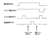
垂直駆動回路16は、例えばシフトレジスタなどによって構成され、画素アレイ部12の各画素11を行単位で選択するとともに、選択行の画素11に対して転送制御線13−1〜13−mを通して転送信号TRFを、リセット制御線14−1〜14−mを通してリセット信号RSTをそれぞれ与える。ここで、画素11の行単位での選択は、垂直走査に同期して垂直駆動回路16から選択信号SELが電源制御回路(図示せず)に与えられ、これに応答して当該電源制御回路から選択行の画素11にドレイン電位DRNが供給されることによって行われる。 The vertical drive circuit 16 is configured by a shift register, for example, and selects each pixel 11 of the pixel array unit 12 in units of rows, and transfers the pixels 11 in the selected row through transfer control lines 13-1 to 13-m. The signal TRF is given as a reset signal RST through reset control lines 14-1 to 14-m, respectively. Here, the selection of the pixels 11 in units of rows is performed by a selection signal SEL supplied from a vertical drive circuit 16 to a power supply control circuit (not shown) in synchronization with vertical scanning, and in response to this, from the power supply control circuit. This is performed by supplying the drain potential DRN to the pixels 11 in the selected row.
図2に、選択信号SEL、ドレイン電位DRN、リセット信号RSTおよび転送信号TRFのタイミング関係を示す。選択信号SELに基づいて画素11の行単位での選択が行われる。そして、選択行において、リセット信号RSTが画素11に与えられることによりFD部の電位がドレイン電位DRNにリセットされ、そのリセット後のFD部の電位がリセットレベルとして増幅トランジスタQ12を介して垂直信号線15−1〜15−nに出力される。その後、転送信号RTFが画素11に与えられることによって、フォトダイオードPDで光電変換された信号電荷がFD部に転送され、その転送後のFD部の電位が信号レベルとして増幅トランジスタQ13を介して垂直信号線15−1〜15−nに出力される。 FIG. 2 shows a timing relationship among the selection signal SEL, the drain potential DRN, the reset signal RST, and the transfer signal TRF. Based on the selection signal SEL, the pixels 11 are selected in units of rows. In the selected row, the reset signal RST is applied to the pixel 11 to reset the potential of the FD portion to the drain potential DRN, and the reset potential of the FD portion is set as a reset level via the amplification transistor Q12. 15-1 to 15-n. Thereafter, the transfer signal RTF is applied to the pixel 11, whereby the signal charge photoelectrically converted by the photodiode PD is transferred to the FD portion, and the potential of the FD portion after the transfer is vertically converted as a signal level through the amplification transistor Q13. It is output to the signal lines 15-1 to 15-n.
垂直信号線15−1〜15−nの一端から取り出される信号は、カラム回路17に供給される。カラム回路17は、例えばCDS(Correlated Double Sampling;相関二重サンプリング)回路およびS/H(サンプルホールド)回路等の信号処理回路によって構成されており、水平ブランキング期間中に画素アレイ部12の例えば2つの選択行の各画素11から出力されるリセットレベルと信号レベルとを列ごとに取り込み、これらレベルの差を取ることによって画素11の固定パターンノイズを除去する処理を行うとともに、例えば2行分の画素の電荷をサンプルホールドする。
A signal extracted from one end of each of the vertical signal lines 15-1 to 15-n is supplied to the
図3に、カラム回路17におけるS/H回路部分の1列分の構成の一例を示す。図3から明らかなように、1列分のカラム回路17のS/H回路部分は、画素アレイ部12の例えば2行分の画素から読み出され、上記CDS回路によってノイズ除去処理された2系統の電荷についてサンプルホールドするために、垂直信号線15と基準電位、例えば接地電位との間に、サンプリングスイッチ31−1およびキャパシタ32−1が直列に接続されるとともに、サンプリングスイッチ31−2およびキャパシタ32−2が直列に接続された構成となっている。そして、サンプリングスイッチ31−1,31−2は、垂直信号線15を介して供給される2行分の画素の信号をそれぞれサンプリングしてキャパシタ32−1,32−2に蓄える。
FIG. 3 shows an example of the configuration of one column of the S / H circuit portion in the
カラム回路17が2系統の電荷を処理するのに対応して、2本の水平信号線21−1,21−2が配線されている。また、サンプリングスイッチ31−1およびキャパシタ32−1の共通接続ノードN11と一方の水平信号線21−1との間に水平選択スイッチ22−1が接続され、サンプリングスイッチ31−2およびキャパシタ32−2の共通接続ノードN12と他方の水平信号線21−1との間に水平選択スイッチ22−2が接続されている。これら水平選択スイッチ22−1,22−2は、水平走査回路18および水平選択スイッチ制御回路19と共に水平駆動回路を構成している。
Two horizontal signal lines 21-1 and 21-2 are wired correspondingly to the
水平走査回路18は、例えばシフトレジスタによって構成され、水平走査期間(有効画素期間)において水平走査パルスφH1〜φHnを順に出力する。水平選択スイッチ制御回路19は、水平デコーダ18から順に出力される水平走査パルスφH1〜φHnに同期して、2系統のスイッチ制御パルスφS1−1,φS1−2〜φSn−1,φSn−2を順次出力し、水平選択スイッチ22−1,22−2を駆動制御する。水平選択スイッチ22−1,22−2は、スイッチ制御パルスφS1−1,φS1−2〜φSn−1,φSn−2が与えられることで、オン(閉)状態となってキャパシタ32−1,32−2にそれぞれ蓄えられている電荷を、水平信号線21−1,21−2を介して出力回路部20に供給する。
The horizontal scanning circuit 18 is constituted by, for example, a shift register, and sequentially outputs horizontal scanning pulses φH1 to φHn in the horizontal scanning period (effective pixel period). The horizontal selection
図3は、S/H回路部分の1列分の構成とともに、出力回路部20の構成の一例を示す回路図である。
FIG. 3 is a circuit diagram showing an example of the configuration of the
図3から明らかなように、出力回路部20は、水平信号線21−1,21−2にそれぞれ対応して設けられた2つの出力回路、例えば電荷−電圧変換アンプ23−1,23−2と、これら電荷−電圧変換アンプ23−1,23−2の出力側に設けられたS/H回路24−1,24−2と、電荷−電圧変換アンプ23−1,23−2の入力端子同士を選択的に短絡するスイッチ25と、電荷−電圧変換アンプ23−1,23−2の出力端子同士を選択的に短絡するスイッチ26とを有する構成となっている。ここで、スイッチ26は必須のものではない。その理由については後で詳述する。
As is apparent from FIG. 3, the
電荷−電圧変換アンプ23−1は、水平信号線21−1の出力端に反転(−)入力端子が接続され、非反転(+)入力端子に参照電圧Vref が与えられるオペアンプ41と、このオペアンプ41の反転入力端子と出力端子との間に直列接続されたスイッチ42a、フィードバックキャパシタ43およびスイッチ42bと、オペアンプ41の反転入力端子と出力端子との間に接続されたリセットスイッチ44とを有する構成となっており、水平信号線21−1を介して供給される電荷を電圧に変換する。なお、スイッチ42a、フィードバックキャパシタ43およびスイッチ42bは、電荷−電圧変換アンプ23−1のゲインを任意に設定し得るように、k組(kは2以上の整数)設けられている。電荷−電圧変換アンプ23−2も、電荷−電圧変換アンプ23−1と全く同じ構成となっている。
The charge-voltage conversion amplifier 23-1 has an inverting (−) input terminal connected to the output terminal of the horizontal signal line 21-1, and an
S/H回路24−1,24−2は、電荷−電圧変換アンプ23−1,23−2の各出力信号のデータ部をサンプルホールドする。このS/H回路24−1,24−2の各ホールドデータ(画素データ)は、画素11で光電変換された電荷に応じた画素信号(アナログ信号)として2系統の出力端子27−1,27−2から導出される。スイッチ25,26は互いに連動し、垂直方向の画素加算を行って低解像度で画素情報の読出しを行う駆動モードの際に、当該駆動モードを指定するモード信号に応答してオン(閉)状態となり、電荷−電圧変換アンプ23−1,23−2の入力端子同士および出力端子同士をそれぞれ短絡する。
The S / H circuits 24-1 and 24-2 sample and hold the data portions of the output signals of the charge-voltage conversion amplifiers 23-1 and 23-2. Each hold data (pixel data) of the S / H circuits 24-1 and 24-2 is output as two pixel output terminals 27-1 and 27 as pixel signals (analog signals) corresponding to the charges photoelectrically converted by the pixels 11. -2. The
ここで、電荷−電圧変換アンプ23−1,23−2における電荷−電圧変換の原理について図4を用いて説明する。ここでは、電荷−電圧変換アンプ23−1を例に挙げて説明するが、電荷−電圧変換アンプ23−2についてもその原理は全く同じである。ある列iのキャパシタ32−1iに蓄えられている電荷に応じた電位をVm、電荷−電圧変換アンプ23−1の参照電位をVref とする。 Here, the principle of charge-voltage conversion in the charge-voltage conversion amplifiers 23-1, 23-2 will be described with reference to FIG. Here, the charge-voltage conversion amplifier 23-1 will be described as an example, but the principle of the charge-voltage conversion amplifier 23-2 is exactly the same. A potential corresponding to the charge stored in the capacitor 32-1i in a certain column i is Vm, and a reference potential of the charge-voltage conversion amplifier 23-1 is Vref.
図5のタイミングチャートにおいて、リセットパルスRPがアクティブ(高レベル)になるリセット相(A)では、リセットパルスRPに応答してリセットスイッチ44がオンすると、オペアンプ41の反転入力端子と非反転入力端子とが短絡される。これにより、電荷−電圧変換アンプ23−1はボルテージフォロワの接続になるため、水平信号線21−1の電位および電荷−電圧変換アンプ23−1の出力電位が参照電位Vref になる。ここで、キャパシタ32−1iの容量値をC1とすると、当該キャパシタ32−1iには、
Q1=Vm・C1
なる電荷量の電荷が蓄えられている。
In the timing chart of FIG. 5, in the reset phase (A) in which the reset pulse RP is active (high level), when the
Q1 = Vm · C1
Is stored.
リセットパルスRPがノンアクティブ(低レベル)になるサンプル相(B)では、リセットスイッチ44がオフし、また水平走査パルスφHに同期したスイッチ制御パルスφSi−1に応答して水平選択スイッチ22−1iがオンするため、キャパシタ32−1iが水平選択スイッチ22−1iを介して水平信号線21−1に接続される。このとき、水平信号線21−1の電位は、電荷−電圧変換アンプ23−1によって参照電位Vref に保たれるため、キャパシタ32−1iの電荷量は、電荷量Q1から
Q2=Vref ・C1
なる電荷量Q2に変化する。
In the sample phase (B) in which the reset pulse RP becomes inactive (low level), the
To a charge amount Q2.
この電荷量の変化量(差分量)ΔQ(=Q1−Q2)が電荷−電圧変換アンプ23−1のフィードバックキャパシタ43のところに現れる。その結果、フィードバックキャパシタ43の容量値をC2(フィードバックキャパシタ43−1〜43−kのいずれか1つの容量値、または複数の組み合わせの合成容量値)とすると、キャパシタ32−1iに蓄えられた電荷が次式で表される電圧Vout に変換される。
Vout =Vref +{(C1/C2)・(Vref −Vm)}
The change amount (difference amount) ΔQ (= Q1−Q2) of the charge amount appears at the
Vout = Vref + {(C1 / C2). (Vref−Vm)}
図3に説明を戻す。本実施形態に係る固体撮像装置では、キャパシタ32−1,32−2および電荷−電圧変換アンプ23−1,23−2を2系統有する構成となっているために、画素情報を高速に読み出す駆動モードを採る必要がある場合には、スイッチ25,26を共にオフ状態にし、出力回路である電荷−電圧変換アンプ23−1,23−2の入力端子同士および出力端子同士をそれぞれ非短絡状態にして2系統の回路系を二線出力という形で利用することにより、アナログ出力端子27−1,27−2から2行分のアナログ画素信号を独立に並行して読み出すことが出来る。
Returning to FIG. The solid-state imaging device according to the present embodiment has a configuration including two systems of capacitors 32-1 and 32-2 and charge-voltage conversion amplifiers 23-1 and 23-2. When it is necessary to adopt the mode, both the
一方、低解像度で読出しを行う駆動モードを採るときには、同じ回路系を使って垂直方向における画素加算を行うことが出来る。具体的には、スイッチ25をオンさせて電荷−電圧変換アンプ23−1,23−2の入力端子同士を短絡状態にすることにより垂直方向において2画素の画素加算を行うことが出来る。このように、電荷−電圧変換アンプ23−1,23−2の入力端子同士を短絡することにより、2系統の電荷−電圧変換アンプ23−1,23−2の各オフセットを無視すれば、原理的に、電荷−電圧変換アンプアンプ23−1,23−2の各出力は、2行分のアナログ画像信号が画素ごとに加算され、単なる和ではなく平均値となり、両出力が同じ値になる。
On the other hand, when a driving mode for reading at low resolution is adopted, pixel addition in the vertical direction can be performed using the same circuit system. Specifically, pixel addition of two pixels can be performed in the vertical direction by turning on the
したがって、アナログ出力端子27−1,27−2のどちらか一方から、画素加算して平均化した画素信号を読み出すようにすれば良い。アナログ出力端子27−1,27−2のどちらか一方から読み出すには、一般にスイッチとキャパシタの組み合わせからなるS/H回路24−1,24−2の一方のスイッチのみをオン状態にすれば良い。このとき、オフ状態にある他方のスイッチ側のS/H回路24−1/24−2から見た負荷が軽くなるため、その分だけ高速読出しを行うことが出来る。 Therefore, the pixel signal averaged by pixel addition may be read from either one of the analog output terminals 27-1 and 27-2. In order to read from either one of the analog output terminals 27-1 and 27-2, it is only necessary to turn on only one of the switches of the S / H circuits 24-1 and 24-2 that are generally a combination of a switch and a capacitor. . At this time, the load as viewed from the S / H circuit 24-1-24-2 on the other switch side in the off state is reduced, so that high-speed reading can be performed correspondingly.
さらに、スイッチ25に連動させてスイッチ26をもオンさせ、電荷−電圧変換アンプ23−1,23−2の出力端子同士をも短絡することにより、2系統の電荷−電圧変換アンプ23−1,23−2にそれぞれオフセットがあったとしても、これらオフセットを打ち消した平均値を出力することが出来る。すなわち、2系統の電荷−電圧変換アンプ23−1,23−2の入力端子同士および出力端子同士をそれぞれ短絡することにより、これら2つの電荷−電圧変換アンプアンプ23−1,23−2が大きな1個の電荷−電圧変換アンプとして働くことになる。
Further, the
ただし、低解像度で読出しを行う駆動モードのときでも、電荷−電圧変換アンプ23−1,23−2の後段にある2系統のS/H回路24−1,24−2の各スイッチを両方ともオン状態にして、アナログ出力端子27−1,27−2の両方から同じ値の平均値を読み出すことも可能である。このように、2系統のS/H回路24−1,24−2の各スイッチを両方ともオン状態にしておけば、電荷−電圧変換アンプ23−1,23−2から見た負荷が二線出力として使う駆動モードの場合と全く同じになるため、2つの駆動モードで違う負荷状態を想定したアンプの設計を行う必要が無くなり、その分だけアンプの設計が容易になる。 However, even in the drive mode in which reading is performed at a low resolution, both switches of the two systems of S / H circuits 24-1 and 24-2 in the subsequent stage of the charge-voltage conversion amplifiers 23-1 and 23-2 are set. It is also possible to read the average value of the same value from both the analog output terminals 27-1 and 27-2 in the ON state. In this way, if the switches of the two systems of S / H circuits 24-1 and 24-2 are both turned on, the load viewed from the charge-voltage conversion amplifiers 23-1 and 23-2 is two lines. Since it is exactly the same as the case of the drive mode used as an output, it is not necessary to design an amplifier assuming different load states in the two drive modes, and the design of the amplifier is facilitated accordingly.
上述したように、複数行、例えば2行の各画素の電荷を列ごとに蓄える2つのキャパシタ32−1,32−2を有するとともに、これらキャパシタ32−1,32−2の各々に蓄えられた電荷に応じたアナログ信号をそれぞれ出力する2つの電荷−電圧変換アンプ23−1,23−2を備えたMOS型固体撮像装置において、2つの電荷−電圧変換アンプ23−1,23−2の入力端子同士を選択的に短絡するスイッチ25を設け、好ましくは出力端子同士を選択的に短絡するスイッチ26をも設けることにより、スイッチ25,26を非短絡状態(オフ状態)にして2つの電荷−電圧変換アンプ23−1,23−2から独立にアナログ信号を読み出す第1の駆動モードと、スイッチ25,26を短絡状態(オン状態)にして2つの電荷−電圧変換アンプ23−1,23−2から各アナログ信号の平均値を読み出す第2の駆動モードとの2つのモードでの駆動が選択的に可能となる。
As described above, there are two capacitors 32-1 and 32-2 that store the charge of each pixel in a plurality of rows, for example, two rows for each column, and the capacitors 32-1 and 32-2 are stored in each of the capacitors 32-1 and 32-2. In a MOS type solid-state imaging device including two charge-voltage conversion amplifiers 23-1 and 23-2 that respectively output analog signals corresponding to charges, input of the two charge-voltage conversion amplifiers 23-1 and 23-2
そして、第1の駆動モードでは、スイッチ25,26を共にオフ状態にして電荷−電圧変換アンプ23−1,23−2の入力端子同士および出力端子同士をそれぞれ非短絡状態にすることにより、2系統の回路系を二線出力という形で利用し、アナログ出力端子27−1,27−2から2行分のアナログ画像信号を独立に並行して読み出すことが出来る。このように、二線出力の形態を採ることにより、静止画モードなど全画素の画素情報を読み出す際に高速読出しを実現出来る。ただし、二線出力の形態に限らず、2系統のキャパシタ32−1,32−2および2つの電荷−電圧変換アンプ23−1,23−2の一方のみを使って一線出力の形態を採ることも可能である。
In the first drive mode, both the
一方、第2の駆動モードでは、スイッチ25をオン状態にして電荷−電圧変換アンプ23−1,23−2の入力端子同士を短絡状態にすることにより、2行分のアナログ画素信号を画素ごとに加算し、単なる和ではなく平均値として読み出すことが出来る。さらに、スイッチ26をもオン状態にして電荷−電圧変換アンプ23−1,23−2の出力端子同士をも短絡状態にすることにより、2系統の電荷−電圧変換アンプ23−1,23−2にそれぞれオフセットがあったとしても、これらオフセットを打ち消すことが出来るため、オフセットが乗らない平均値を出力することが出来る。このように、垂直方向において2画素加算を行うことにより、低解像度の読出しを実現出来る。
On the other hand, in the second drive mode, the
なお、上記実施形態では、キャパシタ32−1,32−2および電荷−電圧変換アンプ23−1,23−2を2系統設けた場合を例に挙げて説明したが、2系統に限られるものではなく、3系統以上設けて垂直方向において3画素以上の画素加算を行ってさらに低解像度で読出しを行うようにすることも可能である。この場合にも、f個(fは3以上の整数)の電荷−電圧変換アンプ23−1〜23−fの入力端子間および出力端子間にそれぞれスイッチを設けることにより、第1の駆動モードではf線出力、第2の駆動モードでは垂直方向におけるf画素加算をそれぞれ実現できる。 In the above embodiment, the case where two systems of capacitors 32-1 and 32-2 and charge-voltage conversion amplifiers 23-1 and 23-2 are provided has been described as an example. However, the present invention is not limited to two systems. Alternatively, it is possible to provide three or more systems and perform pixel addition of three or more pixels in the vertical direction to perform readout at a lower resolution. Also in this case, in the first drive mode, switches are provided between the input terminals and the output terminals of the f (f is an integer of 3 or more) charge-voltage conversion amplifiers 23-1 to 23-f. In the f-line output and the second drive mode, f pixel addition in the vertical direction can be realized.
因みに、上記実施形態では、垂直方向における画素加算についてのみ説明したが、水平方向における画素加算については周知の技術を適用し、水平走査の際に、水平走査回路18から複数列分の水平走査パルスφHを同時にアクティブにして、複数の列に同時にアクセスを行うことにより、水平信号線21−1,21−2上において水平方向(横方向)の複数画素分の情報を加算することが出来る。 Incidentally, in the above embodiment, only the pixel addition in the vertical direction has been described, but a known technique is applied to the pixel addition in the horizontal direction, and horizontal scanning pulses for a plurality of columns are applied from the horizontal scanning circuit 18 during horizontal scanning. By simultaneously activating φH and simultaneously accessing a plurality of columns, it is possible to add information for a plurality of pixels in the horizontal direction (lateral direction) on the horizontal signal lines 21-1 and 21-2.
また、上記実施形態では、キャパシタ32−1,32−2の各々に蓄えられた電荷に応じたアナログ信号をそれぞれ出力する出力回路として、電荷を電圧に変換する電荷−電圧変換アンプ23−1,23−2を用いた場合を例に挙げて説明したが、電荷−電圧変換アンプに限られるものではなく、例えば図6に示すように、参照電圧Vrefを非反転入力とするオペアンプ51と、当該オペアンプ51の非反転入力端子に接続された入力抵抗52と、オペアンプ51の出力端子と非反転入力端子との間に接続された帰還抵抗53とを有する構成の電流−電圧変換アンプ50を用いることも可能である。
In the above-described embodiment, as output circuits that output analog signals corresponding to the charges stored in the capacitors 32-1 and 32-2, respectively, charge-voltage conversion amplifiers 23-1 that convert charges into voltages, However, the present invention is not limited to the charge-voltage conversion amplifier. For example, as shown in FIG. 6, an
この電流−電圧変換アンプ50において、帰還抵抗53の抵抗値をRとすると、キャパシタに蓄えられた電荷に応じた電流Iが入力抵抗52に流れ込むことにより、オペアンプ51の出力電圧Vout は、
Vout =I・R
となる。
In this current-voltage conversion amplifier 50, when the resistance value of the
Vout = IR
It becomes.
ここで、入力抵抗52は発振防止のためのものであり、演算には寄与しない。この電流−電圧変換アンプ50を出力回路として用い、第2の駆動モードで入力端子同士および出力端子同士を短絡することで、2つの帰還抵抗53−1,53−2が並列に接続された状態となり、合成抵抗値がR/2となるため、キャパシタ32−1,32−2の各々に蓄えられた電荷に応じた電流が同じと仮定すると、このときの出力電圧Vout も、
Vout =2I・(R/2)=I・R
となり、垂直方向における2画素の情報を加算して平均化したものとなる。
Here, the input resistor 52 is for preventing oscillation and does not contribute to the calculation. Using this current-voltage conversion amplifier 50 as an output circuit, the two feedback resistors 53-1 and 53-2 are connected in parallel by short-circuiting the input terminals and the output terminals in the second drive mode. Since the combined resistance value is R / 2, assuming that the currents corresponding to the charges stored in the capacitors 32-1 and 32-2 are the same, the output voltage Vout at this time is
Vout = 2I · (R / 2) = I · R
Thus, the information of two pixels in the vertical direction is added and averaged.
また、上記実施形態では、キャパシタ32−1,32−2および電荷−電圧変換アンプ23−1,23−2を2本の水平信号線21−1,21−2の各々に対応して設け、これら水平信号線21−1,21−2を通してキャパシタ32−1,32−2からそれぞれ出力される電荷を電荷−電圧変換アンプ23−1,23−2でそれぞれ電圧に変換する構成のMOS型固体撮像装置に適用した場合を例に挙げて説明したが、これ以外にも、例えばノイズ低減を目的として、キャパシタ32−1,32−2および電荷−電圧変換アンプ23−1,23−2を垂直信号線15−1〜15−nごとに設け、キャパシタ32−1,32−2からそれぞれ出力される電荷を電荷−電圧変換アンプ23−1,23−2で電圧に変換して水平信号線21−1,21−2に出力する構成のMOS型固体撮像装置に適用にも同様に適用することが可能である。 In the above-described embodiment, the capacitors 32-1 and 32-2 and the charge-voltage conversion amplifiers 23-1 and 23-2 are provided corresponding to the two horizontal signal lines 21-1 and 21-2, A MOS type solid-state structure in which charges output from the capacitors 32-1 and 32-2 through the horizontal signal lines 21-1 and 21-2 are converted into voltages by the charge-voltage conversion amplifiers 23-1 and 23-2, respectively. Although the case where the present invention is applied to the imaging apparatus has been described as an example, the capacitors 32-1 and 32-2 and the charge-voltage conversion amplifiers 23-1 and 23-2 are vertically arranged for the purpose of reducing noise, for example. Provided for each of the signal lines 15-1 to 15-n, the charges output from the capacitors 32-1 and 32-2 are converted into voltages by the charge-voltage conversion amplifiers 23-1 and 23-2, and the horizontal signal line 21 is converted. -1, Also applied to the MOS type solid-state imaging device configured to output 1-2 can be similarly applied to.
この場合には、水平信号線21−1,21−2にはS/H回路24−1,24−2だけが設けられる。また、スイッチ25については垂直信号線15−1〜15−nごとに2つの電荷−電圧変換アンプ23−1,23−2の入力端子間に設け、スイッチ26については2本の水平信号線21−1,21−2間に設けることで、第2の駆動モードの際に、垂直信号線15−1〜15−nごとに設けられた2つの電荷−電圧変換アンプ23−1,23−2について、入力端子同士および出力端子同士を短絡状態にすることができるため、上記実施形態の場合と同様の作用効果を得ることができる。
In this case, only the S / H circuits 24-1 and 24-2 are provided on the horizontal signal lines 21-1 and 21-2. The
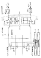
さらには、上記実施形態では、画素11ごとに光電変換して得た電荷を電気信号に変換した後垂直信号線15−1〜15−nに読み出し、しかる後水平スキャンによって出力する水平スキャン方式のMOS構成のMOS型固体撮像装置に適用した場合を例に挙げて説明したが、図7に示すように、画素61で光電変換して得た電荷を垂直画素列ごとに配された垂直転送部(垂直CCD)62−1〜62−nによって垂直転送した後、各垂直画素列毎に垂直転送部62−1〜62−nの後段に設けられた電荷検出部(例えば、電荷−電圧変換部)63−1〜63−nで電気信号に変換して垂直信号線64−1〜64−nを通して読み出し、しかる後水平スキャンによって出力する水平スキャン方式のCCD(Charge Coupled Device)型固体撮像装置にも同様に適用することができる。なお、図7において、カラム回路17、水平走査回路18、水平選択スイッチ制御回路10および出力回路部20の構成については、図1の場合と同じである。
Furthermore, in the above-described embodiment, the charge obtained by photoelectric conversion for each pixel 11 is converted into an electrical signal, read out to the vertical signal lines 15-1 to 15-n, and then output by horizontal scanning. A case where the present invention is applied to a MOS type solid-state imaging device having a MOS configuration has been described as an example. As shown in FIG. 7, a vertical transfer unit in which charges obtained by photoelectric conversion in pixels 61 are arranged for each vertical pixel column. (Vertical CCD) After the vertical transfer by 62-1 to 62-n, a charge detection unit (for example, a charge-voltage conversion unit) provided at the subsequent stage of the vertical transfer unit 62-1 to 62-n for each vertical pixel column In a horizontal scan type CCD (Charge Coupled Device) type solid-state image pickup device which converts into electrical signals at 63-1 to 63-n, reads out the signals through vertical signal lines 64-1 to 64-n, and then outputs them by horizontal scanning. Also It can be applied as. In FIG. 7, the configurations of the
本発明に係る固体撮像装置は、例えば、静止画モード(第1の駆動モード)およびモニタモード(第2の駆動モード)を有するデジタルスチルカメラなどのカメラモジュールの撮像デバイスとして、さらには静止画モードおよびモニタモードを有するカメラ機能を搭載した携帯電話機に代表される携帯端末装置の撮像デバイスとして用いられる。 The solid-state imaging device according to the present invention can be used, for example, as an imaging device of a camera module such as a digital still camera having a still image mode (first drive mode) and a monitor mode (second drive mode). And it is used as an imaging device of a portable terminal device represented by a cellular phone equipped with a camera function having a monitor mode.
11,61…画素、12…画素アレイ部、15−1〜15−n,64−1〜64−n…垂直信号線、16…垂直駆動回路、17…カラム回路、18…水平走査回路、19…水平選択スイッチ制御回路、20…出力回路部、21−1,21−2…水平信号線、22−1,22−2…水平選択スイッチ、23−1,23−2…電荷−電圧変換アンプ、24−1,24−2…サンプルホールド(S/H)回路、25,26…スイッチ、27−1,27−2…アナログ出力端子、31−1,31−2…サンプリングスイッチ、32−1,32−2…キャパシタ、41,51…オペアンプ、44…リセットスイッチ、50…電流−電圧変換アンプ、62−1〜62−n…垂直転送部、63−1〜63−n…電荷検出部
DESCRIPTION OF SYMBOLS 11,61 ... Pixel, 12 ... Pixel array part, 15-1 to 15-n, 64-1 to 64-n ... Vertical signal line, 16 ... Vertical drive circuit, 17 ... Column circuit, 18 ... Horizontal scanning circuit, 19 ... horizontal selection switch control circuit, 20 ... output circuit unit, 21-1, 21-2 ... horizontal signal lines, 22-1, 22-2 ... horizontal selection switch, 23-1, 23-2 ... charge-voltage conversion amplifier , 24-1, 24-2 ... sample hold (S / H) circuit, 25, 26 ... switch, 27-1, 27-2 ... analog output terminal, 31-1, 31-2 ... sampling switch, 32-1 , 32-2...
Claims (21)
前記画素アレイ部から垂直信号線を通して出力される複数行の各画素の電荷を列ごとに蓄える複数のキャパシタと、
前記複数のキャパシタの各々に蓄えられた電荷に応じたアナログ信号をそれぞれ出力する複数の出力回路と、
前記複数の出力回路の入力端子同士を選択的に短絡する第1スイッチ手段と
を備えたことを特徴とする固体撮像装置。 A pixel array unit in which pixels including photoelectric conversion elements are two-dimensionally arranged in a matrix;
A plurality of capacitors for storing charge of each pixel in a plurality of rows output from the pixel array unit through a vertical signal line for each column;
A plurality of output circuits each outputting an analog signal corresponding to the charge stored in each of the plurality of capacitors;
A solid-state imaging device comprising: first switch means for selectively short-circuiting input terminals of the plurality of output circuits.
ことを特徴とする請求項1記載の固体撮像装置。 The solid-state imaging device according to claim 1, further comprising second switch means for selectively short-circuiting output terminals of the plurality of output circuits.
ことを特徴とする請求項1記載の固体撮像装置。 The plurality of capacitors and the plurality of output circuits are provided corresponding to each of a plurality of horizontal signal lines, and charges output from the plurality of capacitors through the plurality of horizontal signal lines are output to the plurality of outputs. The solid-state imaging device according to claim 1, wherein each circuit converts the voltage into a voltage.
ことを特徴とする請求項1記載の固体撮像装置。 The plurality of capacitors and the plurality of output circuits are provided corresponding to each of a plurality of horizontal signal lines, and currents output from the plurality of capacitors according to charges through the plurality of horizontal signal lines are respectively provided. The solid-state imaging device according to claim 1, wherein each of the plurality of output circuits converts the voltage into a voltage.
ことを特徴とする請求項1記載の固体撮像装置。 The plurality of capacitors and the plurality of output circuits are provided for each of the vertical signal lines, and charges respectively output from the plurality of capacitors are converted into voltages by the plurality of output circuits, respectively, thereby generating a plurality of horizontal signals. The solid-state imaging device according to claim 1, wherein the solid-state imaging device outputs to a line.
前記画素アレイ部から垂直信号線を通して出力される複数行の各画素の電荷を列ごとに蓄える複数のキャパシタと、
前記複数のキャパシタの各々に蓄えられた電荷に応じたアナログ信号をそれぞれ出力する複数の出力回路と、
前記複数の出力回路の入力端子同士を選択的に短絡する第1スイッチ手段とを備えた固体撮像装置であって、
前記第1スイッチ手段を非短絡状態にして前記複数の出力回路から独立にアナログ信号を読み出す第1の駆動モードと、
前記第1スイッチ手段を短絡状態にして前記複数の出力回路から各アナログ信号の平均値を読み出す第2の駆動モードと
を有することを特徴とする固体撮像装置。 A pixel array unit in which pixels including photoelectric conversion elements are two-dimensionally arranged in a matrix;
A plurality of capacitors for storing charge of each pixel in a plurality of rows output from the pixel array unit through a vertical signal line for each column;
A plurality of output circuits each outputting an analog signal corresponding to the charge stored in each of the plurality of capacitors;
A solid-state imaging device comprising first switch means for selectively short-circuiting input terminals of the plurality of output circuits,
A first drive mode for reading an analog signal independently from the plurality of output circuits by setting the first switch means in a non-short-circuit state;
And a second drive mode for reading out an average value of each analog signal from the plurality of output circuits with the first switch means short-circuited.
ことを特徴とする請求項6記載の固体撮像装置。 The solid-state imaging device according to claim 6, further comprising second switch means for selectively short-circuiting the output terminals of the plurality of output circuits in conjunction with the first switch means.
前記画素アレイ部から垂直信号線を通して出力される複数行の各画素の電荷を列ごとに蓄える複数のキャパシタと、
前記複数のキャパシタの各々に蓄えられた電荷に応じたアナログ信号をそれぞれ出力する複数の出力回路と、
前記複数の出力回路の入力端子同士を選択的に短絡する第1スイッチ手段とを備えた固体撮像装置の駆動方法であって、
前記第1スイッチ手段を非短絡状態にして前記複数の出力回路から独立にアナログ信号を読み出す
ことを特徴とする固体撮像装置の駆動方法。 A pixel array unit in which pixels including photoelectric conversion elements are two-dimensionally arranged in a matrix;
A plurality of capacitors for storing charge of each pixel in a plurality of rows output from the pixel array unit through a vertical signal line for each column;
A plurality of output circuits each outputting an analog signal corresponding to the charge stored in each of the plurality of capacitors;
A solid-state imaging device driving method comprising: first switch means for selectively short-circuiting input terminals of the plurality of output circuits,
A method for driving a solid-state imaging device, wherein the first switch means is placed in a non-short-circuited state and analog signals are read independently from the plurality of output circuits.
ことを特徴とする請求項8記載の固体撮像装置の駆動方法。 The solid-state imaging device according to claim 8, further comprising second switch means for selectively short-circuiting the output terminals of the plurality of output circuits in conjunction with the first switch means. Device driving method.
ことを特徴とする請求項8記載の固体撮像装置の駆動方法。 The solid-state imaging device driving method according to claim 8, wherein the analog signal is read from one output circuit of the plurality of output circuits.
ことを特徴とする請求項8記載の固体撮像装置の駆動方法。 The method for driving a solid-state imaging device according to claim 8, wherein the analog signal is read in parallel from each of the plurality of output circuits.
前記画素アレイ部から垂直信号線を通して出力される複数行の各画素の電荷を列ごとに蓄える複数のキャパシタと、
前記複数のキャパシタの各々に蓄えられた電荷に応じたアナログ信号をそれぞれ出力する複数の出力回路と、
前記複数の出力回路の入力端子同士を選択的に短絡する第1スイッチ手段とを備えた固体撮像装置の駆動方法であって、
前記第1スイッチ手段を短絡状態にして前記複数の出力回路から各アナログ信号の平均値を読み出す
ことを特徴とする固体撮像装置の駆動方法。 A pixel array unit in which pixels including photoelectric conversion elements are two-dimensionally arranged in a matrix;
A plurality of capacitors for storing charge of each pixel in a plurality of rows output from the pixel array unit through a vertical signal line for each column;
A plurality of output circuits each outputting an analog signal corresponding to the charge stored in each of the plurality of capacitors;
A solid-state imaging device driving method comprising: first switch means for selectively short-circuiting input terminals of the plurality of output circuits,
A solid-state imaging device driving method, wherein the first switch means is short-circuited and an average value of each analog signal is read from the plurality of output circuits.
ことを特徴とする請求項12記載の固体撮像装置の駆動方法。 The solid state imaging device according to claim 12, further comprising second switch means for selectively short-circuiting output terminals of the plurality of output circuits in conjunction with the first switch means. Driving method of imaging apparatus.
ことを特徴とする請求項12記載の固体撮像装置の駆動方法。 The method of driving a solid-state imaging device according to claim 12, wherein the average value is read from all of the plurality of output circuits.
ことを特徴とする請求項12記載の固体撮像装置の駆動方法。 The method for driving a solid-state imaging device according to claim 12, wherein the average value is read from one output circuit of the plurality of output circuits, and the output side of the remaining output circuits is cut off.
前記画素アレイ部から垂直信号線を通して出力される複数行の各画素の電荷を列ごとに蓄える複数のキャパシタと、
前記複数のキャパシタの各々に蓄えられた電荷に応じたアナログ信号をそれぞれ出力する複数の出力回路と、
前記複数の出力回路の入力端子同士を選択的に短絡する第1スイッチ手段とを備えた固体撮像装置の駆動方法であって、
前記第1スイッチ手段を非短絡状態にして前記複数の出力回路から独立にアナログ信号を読み出す第1の駆動モードと、
前記第1スイッチ手段を短絡状態にして前記複数の出力回路から各アナログ信号の平均値を読み出す第2の駆動モードと
の2つのモードでの駆動が選択的に可能である
ことを特徴とする固体撮像装置の駆動方法。 A pixel array unit in which pixels including photoelectric conversion elements are two-dimensionally arranged in a matrix;
A plurality of capacitors for storing charge of each pixel in a plurality of rows output from the pixel array unit through a vertical signal line for each column;
A plurality of output circuits each outputting an analog signal corresponding to the charge stored in each of the plurality of capacitors;
A solid-state imaging device driving method comprising: first switch means for selectively short-circuiting input terminals of the plurality of output circuits,
A first drive mode for reading an analog signal independently from the plurality of output circuits by setting the first switch means in a non-short-circuit state;
The first switch means is short-circuited and can be selectively driven in two modes: a second drive mode in which an average value of each analog signal is read from the plurality of output circuits. Driving method of imaging apparatus.
ことを特徴とする請求項16記載の固体撮像装置の駆動方法。 The solid-state image pickup device further includes second switch means for selectively short-circuiting output terminals of the plurality of output circuits in conjunction with the first switch means. Driving method of imaging apparatus.
ことを特徴とする請求項16記載の固体撮像装置の駆動方法。 The method of driving a solid-state imaging device according to claim 16, wherein in the first driving mode, the analog signal is read from one output circuit of the plurality of output circuits.
ことを特徴とする請求項16記載の固体撮像装置の駆動方法。 The solid-state imaging device driving method according to claim 16, wherein in the first driving mode, the analog signal is read out in parallel from each of the plurality of output circuits.
ことを特徴とする請求項16記載の固体撮像装置の駆動方法。 The solid-state imaging device driving method according to claim 16, wherein, in the second driving mode, the average value is read from all of the plurality of output circuits.
ことを特徴とする請求項16記載の固体撮像装置の駆動方法。
The solid state according to claim 16, wherein in the second drive mode, the average value is read from one output circuit of the plurality of output circuits, and the output side of the remaining output circuits is set in a cutoff state. Driving method of imaging apparatus.
Priority Applications (8)
| Application Number | Priority Date | Filing Date | Title |
|---|---|---|---|
| JP2004036507A JP2005229373A (en) | 2004-02-13 | 2004-02-13 | Solid imaging device and driving method thereof |
| TW094103843A TWI257244B (en) | 2004-02-13 | 2005-02-05 | Solid-state image pickup device and driving method therefor |
| CN200510069772A CN100592526C (en) | 2004-02-13 | 2005-02-08 | Solid-state image pickup device and driving method therefor |
| US11/053,719 US7595828B2 (en) | 2004-02-13 | 2005-02-08 | Solid-state image pickup device and driving method therefor |
| EP07024114A EP1898628B1 (en) | 2004-02-13 | 2005-02-11 | Solid-state image pickup device |
| DE602005027514T DE602005027514D1 (en) | 2004-02-13 | 2005-02-11 | A driving method for a solid-state imaging device |
| EP05002973A EP1564986B1 (en) | 2004-02-13 | 2005-02-11 | Driving method for a solid-state image pickup device |
| KR1020050011985A KR101122424B1 (en) | 2004-02-13 | 2005-02-14 | Solid-state image pickup device and driving method therefor |
Applications Claiming Priority (1)
| Application Number | Priority Date | Filing Date | Title |
|---|---|---|---|
| JP2004036507A JP2005229373A (en) | 2004-02-13 | 2004-02-13 | Solid imaging device and driving method thereof |
Related Child Applications (1)
| Application Number | Title | Priority Date | Filing Date |
|---|---|---|---|
| JP2009019192A Division JP4788782B2 (en) | 2009-01-30 | 2009-01-30 | Solid-state imaging device and driving method of solid-state imaging device |
Publications (1)
| Publication Number | Publication Date |
|---|---|
| JP2005229373A true JP2005229373A (en) | 2005-08-25 |
Family
ID=34697919
Family Applications (1)
| Application Number | Title | Priority Date | Filing Date |
|---|---|---|---|
| JP2004036507A Pending JP2005229373A (en) | 2004-02-13 | 2004-02-13 | Solid imaging device and driving method thereof |
Country Status (7)
| Country | Link |
|---|---|
| US (1) | US7595828B2 (en) |
| EP (2) | EP1564986B1 (en) |
| JP (1) | JP2005229373A (en) |
| KR (1) | KR101122424B1 (en) |
| CN (1) | CN100592526C (en) |
| DE (1) | DE602005027514D1 (en) |
| TW (1) | TWI257244B (en) |
Cited By (1)
| Publication number | Priority date | Publication date | Assignee | Title |
|---|---|---|---|---|
| JP2020067834A (en) * | 2018-10-24 | 2020-04-30 | 株式会社ジャパンディスプレイ | Fingerprint detection device and display device equipped with fingerprint detection device |
Families Citing this family (15)
| Publication number | Priority date | Publication date | Assignee | Title |
|---|---|---|---|---|
| JP2006014316A (en) * | 2004-06-22 | 2006-01-12 | Samsung Electronics Co Ltd | Improved solid-state image sensor for equalizing sub-sampled analog signals and driving method thereof |
| KR100674957B1 (en) * | 2005-02-23 | 2007-01-26 | 삼성전자주식회사 | Solid state image sensing device and driving method for averaging and sub-sampling analog signals at an arbitrary sub-sampling rate |
| EP1788797B1 (en) * | 2005-11-18 | 2013-06-26 | Canon Kabushiki Kaisha | Solid-state image pickup device |
| JP2007274504A (en) * | 2006-03-31 | 2007-10-18 | Eastman Kodak Co | Digital camera |
| CN101197921B (en) * | 2006-12-07 | 2010-11-03 | 比亚迪股份有限公司 | Image signal sampling circuit and its method |
| JP4305507B2 (en) * | 2006-12-18 | 2009-07-29 | ソニー株式会社 | Imaging device and camera |
| JP4058459B1 (en) * | 2007-03-02 | 2008-03-12 | キヤノン株式会社 | Imaging apparatus and imaging system |
| JP5188221B2 (en) * | 2008-03-14 | 2013-04-24 | キヤノン株式会社 | Solid-state imaging device |
| JP4659868B2 (en) * | 2008-09-19 | 2011-03-30 | キヤノン株式会社 | Solid-state imaging device and imaging system |
| US8212903B2 (en) * | 2009-07-31 | 2012-07-03 | Xerox Corporation | Sensor array with selectable resolution and method thereof |
| JP5235814B2 (en) * | 2009-08-04 | 2013-07-10 | キヤノン株式会社 | Solid-state imaging device |
| EP2367321B1 (en) | 2010-03-05 | 2014-01-22 | Televés, S.A. | Communications system and method |
| US9699395B1 (en) * | 2016-03-17 | 2017-07-04 | Raytheon Company | Imaging circuits and method |
| JP7271131B2 (en) * | 2018-10-24 | 2023-05-11 | キヤノン株式会社 | IMAGING DEVICE AND METHOD OF CONTROLLING IMAGING DEVICE |
| US11082643B2 (en) * | 2019-11-20 | 2021-08-03 | Waymo Llc | Systems and methods for binning light detectors |
Family Cites Families (12)
| Publication number | Priority date | Publication date | Assignee | Title |
|---|---|---|---|---|
| US5790191A (en) * | 1996-03-07 | 1998-08-04 | Omnivision Technologies, Inc. | Method and apparatus for preamplification in a MOS imaging array |
| US5901257A (en) | 1996-05-03 | 1999-05-04 | Omnivision Technologies, Inc. | Single chip color MOS image sensor with two line reading structure and improved color filter pattern |
| JP3466886B2 (en) * | 1997-10-06 | 2003-11-17 | キヤノン株式会社 | Solid-state imaging device |
| US6765613B1 (en) * | 1998-07-22 | 2004-07-20 | Micron Technology, Inc. | Low light sensor signal to noise improvement |
| US7068312B2 (en) * | 2000-02-10 | 2006-06-27 | Minolta Co., Ltd. | Solid-state image-sensing device |
| JP4011818B2 (en) * | 2000-02-29 | 2007-11-21 | キヤノン株式会社 | Semiconductor solid-state imaging device |
| US6952228B2 (en) * | 2000-10-13 | 2005-10-04 | Canon Kabushiki Kaisha | Image pickup apparatus |
| EP1356665A4 (en) | 2000-11-27 | 2006-10-04 | Vision Sciences Inc | Programmable resolution cmos image sensor |
| JP2002330349A (en) * | 2001-04-26 | 2002-11-15 | Fujitsu Ltd | Xy address type solid-state image pickup device |
| US6541751B1 (en) * | 2001-10-03 | 2003-04-01 | Pixim Inc | Time multiplexing image processing functions for noise reduction |
| JP2004153705A (en) * | 2002-10-31 | 2004-05-27 | Matsushita Electric Ind Co Ltd | Amplification type solid-state imaging device and imaging system using the same |
| US7304674B2 (en) * | 2002-11-15 | 2007-12-04 | Avago Technologies General Ip Pte Ltd | Sampling image signals generated by pixel circuits of an active pixel sensor (APS) image sensor in a sub-sampling mode |
-
2004
- 2004-02-13 JP JP2004036507A patent/JP2005229373A/en active Pending
-
2005
- 2005-02-05 TW TW094103843A patent/TWI257244B/en not_active IP Right Cessation
- 2005-02-08 CN CN200510069772A patent/CN100592526C/en not_active Expired - Fee Related
- 2005-02-08 US US11/053,719 patent/US7595828B2/en not_active Expired - Fee Related
- 2005-02-11 EP EP05002973A patent/EP1564986B1/en not_active Expired - Fee Related
- 2005-02-11 EP EP07024114A patent/EP1898628B1/en not_active Expired - Fee Related
- 2005-02-11 DE DE602005027514T patent/DE602005027514D1/en active Active
- 2005-02-14 KR KR1020050011985A patent/KR101122424B1/en not_active IP Right Cessation
Cited By (5)
| Publication number | Priority date | Publication date | Assignee | Title |
|---|---|---|---|---|
| JP2020067834A (en) * | 2018-10-24 | 2020-04-30 | 株式会社ジャパンディスプレイ | Fingerprint detection device and display device equipped with fingerprint detection device |
| WO2020084910A1 (en) * | 2018-10-24 | 2020-04-30 | 株式会社ジャパンディスプレイ | Fingerprint detection device and display device with fingerprint detection device |
| CN112930551A (en) * | 2018-10-24 | 2021-06-08 | 株式会社日本显示器 | Fingerprint detection device and display device with fingerprint detection device |
| US11436859B2 (en) | 2018-10-24 | 2022-09-06 | Japan Display Inc. | Fingerprint detection device and display device with fingerprint detection device |
| JP7222656B2 (en) | 2018-10-24 | 2023-02-15 | 株式会社ジャパンディスプレイ | Fingerprint detection device and display device with fingerprint detection device |
Also Published As
| Publication number | Publication date |
|---|---|
| EP1564986A2 (en) | 2005-08-17 |
| TW200537920A (en) | 2005-11-16 |
| TWI257244B (en) | 2006-06-21 |
| US20050179795A1 (en) | 2005-08-18 |
| CN100592526C (en) | 2010-02-24 |
| EP1564986A3 (en) | 2006-11-22 |
| DE602005027514D1 (en) | 2011-06-01 |
| US7595828B2 (en) | 2009-09-29 |
| EP1564986B1 (en) | 2011-04-20 |
| CN1755936A (en) | 2006-04-05 |
| KR101122424B1 (en) | 2012-03-09 |
| KR20060041926A (en) | 2006-05-12 |
| EP1898628A1 (en) | 2008-03-12 |
| EP1898628B1 (en) | 2011-12-28 |
Similar Documents
| Publication | Publication Date | Title |
|---|---|---|
| KR101122424B1 (en) | Solid-state image pickup device and driving method therefor | |
| JP4609428B2 (en) | Solid-state imaging device, driving method of solid-state imaging device, and imaging device | |
| KR101177140B1 (en) | Solid state imaging device, method of driving solid state imaging device and image pickup apparatus | |
| JP4011818B2 (en) | Semiconductor solid-state imaging device | |
| JP5288965B2 (en) | Solid-state imaging device and driving method thereof | |
| JP4584634B2 (en) | Solid-state imaging device | |
| JP5506450B2 (en) | Solid-state imaging device and driving method of solid-state imaging device | |
| US7750961B2 (en) | Solid-state imaging apparatus using an amplification-type MOS sensor | |
| JP2008042224A (en) | Solid-state imaging device and imaging device | |
| JP5495551B2 (en) | Solid-state imaging device | |
| JP2009141631A (en) | Photoelectric conversion device and image pickup device | |
| JP2007300521A (en) | Solid-state imaging apparatus | |
| JP4533367B2 (en) | Solid-state imaging device | |
| US10791293B2 (en) | Solid-state imaging device, method for driving solid-state imaging device, and electronic apparatus | |
| JP2006032374A (en) | Solid-state imaging apparatus | |
| JP5340643B2 (en) | Solid-state imaging device | |
| TWI497996B (en) | Solid-state imaging device | |
| US8102441B2 (en) | Solid-state imaging apparatus | |
| US8045027B2 (en) | Solid-state imaging apparatus | |
| JP4788782B2 (en) | Solid-state imaging device and driving method of solid-state imaging device | |
| JP2000050164A (en) | Signal processor and image pickup device using the same | |
| US8872951B2 (en) | Method and system for operating an image data collection device | |
| JP4322562B2 (en) | Solid-state imaging device | |
| JP4386296B2 (en) | Semiconductor solid-state imaging device | |
| JP2007116479A (en) | Solid-state imaging apparatus and signal reading method thereof |
Legal Events
| Date | Code | Title | Description |
|---|---|---|---|
| A131 | Notification of reasons for refusal |
Free format text: JAPANESE INTERMEDIATE CODE: A131 Effective date: 20071211 |
|
| A521 | Request for written amendment filed |
Free format text: JAPANESE INTERMEDIATE CODE: A523 Effective date: 20080212 |
|
| A131 | Notification of reasons for refusal |
Free format text: JAPANESE INTERMEDIATE CODE: A131 Effective date: 20080909 |
|
| A521 | Request for written amendment filed |
Free format text: JAPANESE INTERMEDIATE CODE: A523 Effective date: 20081107 |
|
| A02 | Decision of refusal |
Free format text: JAPANESE INTERMEDIATE CODE: A02 Effective date: 20081202 |