JP2005210764A - Drive controller of brushless motor - Google Patents
Drive controller of brushless motor Download PDFInfo
- Publication number
- JP2005210764A JP2005210764A JP2004011416A JP2004011416A JP2005210764A JP 2005210764 A JP2005210764 A JP 2005210764A JP 2004011416 A JP2004011416 A JP 2004011416A JP 2004011416 A JP2004011416 A JP 2004011416A JP 2005210764 A JP2005210764 A JP 2005210764A
- Authority
- JP
- Japan
- Prior art keywords
- commutation
- phase
- brushless motor
- current
- commutation pattern
- Prior art date
- Legal status (The legal status is an assumption and is not a legal conclusion. Google has not performed a legal analysis and makes no representation as to the accuracy of the status listed.)
- Pending
Links
Images


Landscapes
- Power Steering Mechanism (AREA)
- Control Of Motors That Do Not Use Commutators (AREA)
Abstract
Description
本発明は複数の励磁相を有するブラシレスモータの駆動制御装置に関し、特に電動式パワーステアリング装置の駆動源に好適なブラシレスモータの駆動制御装置に関する。 The present invention relates to a drive control device for a brushless motor having a plurality of excitation phases, and more particularly to a drive control device for a brushless motor suitable for a drive source of an electric power steering device.
自動車のパワーステアリング装置の駆動源として用いられているブラシレスモータは、3相以上の励磁相を有するモータであり、その駆動は矩形波状の励磁電流によって行われている。 A brushless motor used as a drive source for a power steering device of an automobile is a motor having three or more excitation phases, and is driven by a rectangular wave-like excitation current.
例えば5相ブラシレスモータの場合、モータ駆動回路は、モータのロータの外周面を電気角で72度ずつ離隔して取り囲むように配設された5相(以下、これらをa相〜e相という)の励磁コイルa〜eに対し、マイクロコンピュータ等の制御回路による制御下で、4相同時に励磁する4相励磁方式により、コイルを1相ずつ順次切替えて矩形波電流で励磁することにより、ロータを回転駆動させている。この4相励磁方式では、モータ電流は5相のうちの4つの相に流れることになるが、各相にバランスよく電流を流すために、各励磁コイルの抵抗は全て等しくなるように形成されている。 For example, in the case of a five-phase brushless motor, the motor drive circuit has five phases (hereinafter referred to as a phase to e phase) arranged so as to surround the outer circumferential surface of the rotor of the motor with an electrical angle of 72 degrees apart. The excitation coils a to e are controlled by a control circuit such as a microcomputer, and the four phases are excited simultaneously, and the coils are sequentially switched one by one and excited by a rectangular wave current. It is driven to rotate. In this four-phase excitation method, the motor current flows in four of the five phases, but in order to flow the current in a balanced manner, the resistances of the respective excitation coils are all made equal. Yes.
このようなモータ駆動回路は、通常10個の電界効果トランジスタ(FET)で構成されている。これら10個のトランジスタは、対応する2個のトランジスタを直列接続して5つの直列トランジスタ回路を形成し、それぞれを電源の正負両端子間に接続すると共に、各直列トランジスタ回路の2個のトランジスタの接続部をそれぞれY字形にスター結線した5個の励磁コイルa〜eの外端に接続することにより、モータのコイル回路と接続している。 Such a motor drive circuit is usually composed of ten field effect transistors (FETs). These 10 transistors are formed by connecting two corresponding transistors in series to form five series transistor circuits, each being connected between the positive and negative terminals of the power source, and the two transistors of each series transistor circuit. By connecting the connecting portions to the outer ends of the five exciting coils a to e that are star-connected in a Y shape, they are connected to the motor coil circuit.
このモータ駆動回路から各励磁コイルへ供給される励磁電流(矩形波)の方向及び長さは、ロータの回転角(電気角)の値に対して例えば図8に示すようになる。即ち、電気角で36度毎に順次1相ずつ励磁コイルを切替え、1つの相コイルを電気角で144度の間励磁することにより、ロータを連続して回転させるようになっている。この図8では、電気角をθとしたとき、0°≦θ<36°,36°≦θ<72°,72°≦θ<108°,108°≦θ<144°,144°≦θ<180°,180°≦θ<216°,216°≦θ<252°,252°≦θ<288°,288°≦θ<324°,324°≦θ<360°の区間をそれぞれ(1),・・・・,(10)で表わしている。 The direction and length of the excitation current (rectangular wave) supplied from the motor drive circuit to each excitation coil are as shown in FIG. 8, for example, with respect to the value of the rotation angle (electrical angle) of the rotor. That is, the rotor is continuously rotated by switching the excitation coil one phase at a time every 36 degrees in electrical angle and exciting one phase coil for 144 degrees in electrical angle. In FIG. 8, when the electrical angle is θ, 0 ° ≦ θ <36 °, 36 ° ≦ θ <72 °, 72 ° ≦ θ <108 °, 108 ° ≦ θ <144 °, 144 ° ≦ θ < 180 °, 180 ° ≦ θ <216 °, 216 ° ≦ θ <252 °, 252 ° ≦ θ <288 °, 288 ° ≦ θ <324 °, 324 ° ≦ θ <360 ° (1),・ ・ ・ ・, (10)
本例の場合、a相の電流は区間(1)及び(2)で正方向に流れ、区間(3)で0、区間(4)〜(7)で負方向に流れ、区間(8)で0、区間(9)から(10)を経て再び区間(1)で正方向に流れる。b相の電流は、区間(1)〜(4)で正方向に流れ、区間(5)で0、区間(6)〜(9)で負方向に流れ、区間(10)で0、そして再び区間(1)で正方向に流れる。c相の電流は、区間(1)で負方向に流れ、区間(2)で0、区間(3)〜(6)で正方向に流れ、区間(7)で0、区間(8)〜(10)を経て再び区間(1)で負方向に流れる。d相の電流は、区間(1)〜(3)で負方向に流れ、区間(4)で0、区間(5)〜(8)で正方向に流れ、区間(9)で0、そして区間(10)から再び負方向に流れる。e相の電流は、区間(1)で0、区間(2)〜(5)で負方向に流れ、区間(6)で0、区間(7)〜(10)で正方向に流れ、再び区間(1)で0となる。従って、区間(1)〜(10)の各境界(電気角で36度毎の切替え時)では、5つの励磁コイルのうちの2つが互いに逆向きに切替えられることになる。 In this example, the a-phase current flows in the positive direction in the sections (1) and (2), 0 in the section (3), in the negative direction in the sections (4) to (7), and in the section (8). 0, it flows in the positive direction again in the section (1) through the sections (9) to (10). The b-phase current flows in the positive direction in sections (1) to (4), 0 in section (5), negative in sections (6) to (9), 0 in section (10), and again It flows in the positive direction in section (1). The c-phase current flows in the negative direction in section (1), 0 in section (2), flows in the positive direction in sections (3)-(6), 0 in section (7), and sections (8)-( After 10), it flows again in the negative direction in section (1). The d-phase current flows in the negative direction in the sections (1) to (3), 0 in the section (4), in the positive direction in the sections (5) to (8), 0 in the section (9), and the section It flows again in the negative direction from (10). The e-phase current is 0 in the section (1), flows in the negative direction in the sections (2) to (5), 0 in the section (6), flows in the positive direction in the sections (7) to (10), and again in the section It becomes 0 in (1). Therefore, two of the five exciting coils are switched in the opposite directions at each boundary of the sections (1) to (10) (when the electrical angle is switched every 36 degrees).
このような励磁電流の切替えは、原理的には、図8に示すような矩形波の立ち上がり又は立ち下がりで表わされるが、実際にはその立ち上がり又は立ち下がり波形は横軸(時間若しくは回転角)に対し直角に変化するのではなく、励磁電流が正方向に立ち上がるまで或いは負方向に立ち下がるまで、ある程度の時間Δt(モータ回路の時定数の3倍位)がかかる。例えば、図8の区間(8)と(9)の境界(電気角で288度)では、a相の電流が0から正の一定値まで立ち上がる一方、d相の電流が正の一定値から0に立ち下がり、b相及びc相の電流は共に“負”の一定値、e相の電流は“正”の一定値であるが、この境界部分の波形の変化を拡大すると図9に示すようになる。そして、5つの相の電流をia,ib,ic,id,ieで表わしたとき、これらの電流の間には下記(1)式の関係がある。
ia +id +ie =−(ib +ic)=I ・・・(1)
このため、例えばa相とd相の電流が変化すると、b,c,e相の電流も変化する。この場合、a相とd相の電流変化率が異なるため、2つの相の電流の合計値が定常値にならず、図9に示すようにb相,c相の電流が変動し、e相の電流も時間Δtの間変化する。これらの電流変動により、過度的なトルク変動が生じてしまう。
Such switching of the excitation current is theoretically expressed by a rising or falling edge of a rectangular wave as shown in FIG. 8, but actually the rising or falling waveform is shown on the horizontal axis (time or rotation angle). However, it takes a certain time Δt (three times the time constant of the motor circuit) until the exciting current rises in the positive direction or falls in the negative direction. For example, at the boundary between sections (8) and (9) in FIG. 8 (electrical angle 288 degrees), the a-phase current rises from 0 to a positive constant value, while the d-phase current rises from a positive constant value to 0. The b-phase and c-phase currents are both “negative” constant values, and the e-phase current is “positive” constant values. When the change in the waveform at this boundary portion is enlarged, as shown in FIG. become. When the currents of the five phases are represented by i a , i b , i c , i d and i e , there is a relationship of the following formula (1) between these currents.
i a + i d + i e = − (i b + i c ) = I (1)
For this reason, for example, when the a-phase and d-phase currents change, the b-, c-, and e-phase currents also change. In this case, since the current change rates of the a phase and the d phase are different, the total value of the currents of the two phases does not become a steady value, and the currents of the b phase and the c phase fluctuate as shown in FIG. The current also changes during the time Δt. These current fluctuations cause excessive torque fluctuations.
このように2つの相の電流の立ち上がりと立ち下がりの電流変化率が異なるのは、次の理由による。 The reason why the current change rates of the rising and falling currents of the two phases are different is as follows.
先ず、モータ駆動回路に供給される電源電圧をVb、スター結線した励磁コイルa〜eの中心接続点の電圧をVnとする。次に、図9において、時間Δt1の区間を(a)、時間Δt2(=Δt−Δt1)の区間を(b)とする。 First, let Vb be the power supply voltage supplied to the motor drive circuit, and let Vn be the voltage at the center connection point of the excitation coils a to e that are star-connected. Next, in FIG. 9, the section of time Δt1 is (a), and the section of time Δt2 (= Δt−Δt1) is (b).
区間(a)では、正から0に切替えられるd相(OFF相)の電流idは、−Vn,コイルの逆起電圧Ed及びモータ回路の時定数に応じた変化率で、モータ駆動回路からモータへの通電電流Iの半分(I/2)から零(0)まで下がる。このとき、OFF相の等価回路に加えられる電圧をVOFFとすると、VOFF =−Vn −Ed <0であり、Vnは近似的にVb/2となる。一方、0から正に切替えられるa相(ON相)の電流iaは、電圧Vb,−Vn、コイルの逆起電圧Ea及びモータ回路の時定数に応じた変化率で零(0)から上昇するが、このときON相の等価回路に加えられる電圧をVONとすると、VON=Vb・Duty1(PWMのデューティ)−Vn−Eaである。 In the section (a), the d-phase (OFF-phase) current i d that is switched from positive to zero has a rate of change corresponding to −Vn, the back electromotive force E d of the coil, and the time constant of the motor circuit. Decreases from half (I / 2) of the current I applied to the motor to zero (0). At this time, if the voltage applied to the OFF-phase equivalent circuit is V OFF , V OFF = −Vn−Ed <0, and Vn is approximately Vb / 2. On the other hand, the current i a of a phase which is positively switched from 0 (ON phase), increase the voltage Vb, -Vn, the change rate according to the time constant of the back electromotive force Ea and the motor circuit of the coil from zero (0) However, if the voltage applied to the ON-phase equivalent circuit is V ON at this time, V ON = Vb · Duty1 (PWM duty) −Vn−Ea.
式で説明すると、OFF相の等価回路により電流idは次の(2)式で表わされる。
id(t)= (I/2)e-t/T+(VOFF/R)(1−e-t/T) ・・・(2)
∴t=0のとき、id =I/2
但し、Tは等価回路の電気的時定数、Rは等価回路の抵抗である。
一方、ON相の等価回路により、電流iaは次の(3)式で表わされる。
Explained by the equation, the current i d is expressed by the following equation (2) by an equivalent circuit of the OFF phase.
i d (t) = (I / 2) e −t / T + (V OFF / R) (1−e −t / T ) (2)
When ∴t = 0, i d = I / 2
Where T is the electrical time constant of the equivalent circuit, and R is the resistance of the equivalent circuit.
On the other hand, the current i a is expressed by the following equation (3) by an ON-phase equivalent circuit.
ia(t)=(VON/R)(1−e-t/T) ・・・(3)
∴t=0のとき、ia =0、 t→∞で、ia =VON/R=I/2
従って、OFF相,ON相の各電流id,iaの変化率は、それぞれ次のようになる。
did(t)/dt =−(1/T)(I/2)e-t/T+(1/T)(VOFF/R)e-t/T
=−(I/2−VOFF/R)(1/T)e-t/T
=−(I/2+Vn/R+Ed/R)(1/T)e-t/T ・・・(4)
dia(t)/dt =(1/T)(VON/R)e-t/T
=(I/2)(1/T)e-t/T ・・・(5)
上記(4)式及び(5)式において、(I/2+Vn/R+Ed/R) >I/2であるから、OFF相の電流変化率の方がON相の電流変化率より大きい。特に等価回路の抵抗Rが小さい場合、電源電圧Vb(≒2Vn)が大きい場合、或いは高速回転時で逆起電圧Edが大きい場合には、OFF相の電流変化率はON相の電流変化率よりかなり大きくなる。従って、OFF相の電流idがI/2から0まで下がる時間(Δt1)よりも、ON相の電流iaが0からI/2まで上がる時間(Δt)の方が長い。その後、区間(b)において、ON相の電流iaが最終的に定常値(I/2)に到達するが、それまでに時間Δt2(モータ回路の時定数の2〜3倍)を要する。従って、切替えられる2つの相の電流の立ち上がりと立ち下がりでは、電流変化率が異なっている。
i a (t) = (V ON / R) (1−e −t / T ) (3)
When ∴t = 0, i a = 0, t → ∞, i a = V ON / R = I / 2
Thus, OFF-phase, the current i d of ON phase, the rate of change of i a, respectively as follows.
di d (t) / dt =-(1 / T) (I / 2) e- t / T + (1 / T) ( VOFF / R) e- t / T
=-(I / 2-V OFF / R) (1 / T) e -t / T
=-(I / 2 + Vn / R + Ed / R) (1 / T) e- t / T (4)
di a (t) / dt = (1 / T) (V ON / R) e -t / T
= (I / 2) (1 / T) e -t / T (5)
In the above equations (4) and (5), since (I / 2 + Vn / R + Ed / R)> I / 2, the OFF phase current change rate is larger than the ON phase current change rate. In particular, when the resistance R of the equivalent circuit is small, the power supply voltage Vb (≈2Vn) is large, or the counter electromotive voltage Ed is large at high speed rotation, the OFF phase current change rate is higher than the ON phase current change rate. It gets quite big. Therefore, the time (Δt) during which the ON-phase current i a rises from 0 to I / 2 is longer than the time (Δt1) during which the OFF-phase current i d falls from I / 2 to 0. Thereafter, in the section (b), the ON-phase current i a finally reaches the steady value (I / 2), but it takes time Δt2 (2 to 3 times the time constant of the motor circuit). Therefore, the current change rate differs between the rising and falling currents of the two phases to be switched.
上述のように従来のモータ駆動回路による励磁電流の制御では、切替える2つの相(例えば図8のa相及びd相)の電流の立ち上がりと立ち下がりの変化率が異なるため、切替えられない相(例えば図8のb相、c相、e相)の電流が変動し、それらの電流変動により過度的なトルク変動が生じてしまう。 As described above, in the excitation current control by the conventional motor drive circuit, since the rate of change of the rising and falling currents of the two phases to be switched (for example, the a phase and the d phase in FIG. 8) are different, the phases that cannot be switched ( For example, the currents of b-phase, c-phase, and e-phase in FIG.
このような問題を解決するものとして、特許文献1(特開2001−268879)に示すものがある。特許文献1では、転流時の電流変化率を制御する電流変化率制御手段を有すると共に、複数の励磁相を有するブラシレスモータの駆動制御装置において、電流変化率制御手段は、転流動作において相電流が過渡状態になっている時間である転流の過渡時間を、ある転流の開始時間から次の転流の開始時間までに要する時間である転流間隔時間の1/2以内に終了させるようにしている。
As a solution to such a problem, there is one disclosed in Patent Document 1 (Japanese Patent Laid-Open No. 2001-268879). In
しかしながら、上述したように立ち上がり相電流と立ち下がり相電流が異なり、転流していない相電流が変化してしまうために各相電流の和が0となり、転流動作において相電流が過渡状態になっている転流の過渡時間を、ある転流の開始時間から次の転流の開始時間までに要する転流間隔時間の1/2以内に終了させるようにモータを駆動制御するだけでは、振動や騒音が発生してしまう問題がある。 However, as described above, the rising phase current and the falling phase current are different, and the phase current that is not commutated changes. Therefore, the sum of the phase currents becomes 0, and the phase current becomes a transient state in the commutation operation. If the motor is driven and controlled so that the transition time of the commutation is completed within half of the commutation interval time required from the start time of one commutation to the start time of the next commutation, vibration or There is a problem that noise is generated.
本発明は上述のような事情からなされたものであり、本発明の目的は、ブラシレスモータにおける電流変動、トルク変動及び騒音の発生を確実に抑制することができ、電動パワーステアリング装置のトルクアシスト装置として適用した場合に、低騒音で操舵フィーリングの良い電動パワーステアリング装置を構築することができるブラシレスモータの駆動制御装置を提供することにある。 The present invention has been made in view of the above circumstances, and an object of the present invention is to reliably suppress the occurrence of current fluctuation, torque fluctuation and noise in a brushless motor, and a torque assist device for an electric power steering apparatus. The present invention is to provide a drive control device for a brushless motor capable of constructing an electric power steering device with low noise and good steering feeling.
本発明は、矩形波状の励磁電流で駆動される複数の励磁相を有するブラシレスモータの駆動制御装置に関し、本発明の上記目的は、前記ブラシレスモータへの電流指令値を算出する電流指令値算出手段と、転流時に予め定められた数値で与えられる各相の転流パターンを生成する転流パターン発生部とを設け、前記転流パターン及び電流指令値に基づいて、前記ブラシレスモータの各相への電流指令値を算出する各相電流指令値算出手段を設けることにより達成される。 The present invention relates to a drive control device for a brushless motor having a plurality of excitation phases driven by a rectangular wave excitation current, and the object of the present invention is to provide a current command value calculation means for calculating a current command value for the brushless motor. And a commutation pattern generator for generating a commutation pattern of each phase given by a predetermined numerical value at the time of commutation, and to each phase of the brushless motor based on the commutation pattern and a current command value This is achieved by providing each phase current command value calculating means for calculating the current command value.
また、本発明の上記目的は、前記転流パターンの2相の和が1又は−1となる数値の組であり、前記転流パターンと前記電流指令値とを乗じて前記各相への電流指令値を算出することにより、或いは前記転流パターンを正弦波波形とすることにより、より効果的に達成される。 The above object of the present invention is a set of numerical values in which the sum of the two phases of the commutation pattern is 1 or −1, and the current to each phase is multiplied by the commutation pattern and the current command value. This is achieved more effectively by calculating a command value or by making the commutation pattern into a sine wave waveform.
本発明のブラシレスモータの駆動制御装置によれば、転流時の転流パターンの2相の和が1又は−1となる数値の組であり、転流パターンと電流指令値とを乗じて各相への電流指令値を算出しており、更には転流パターンを正弦波波形で与えるようにしているので、ブラシレスモータの振動や騒音の低い電流指令値を与えることができる。従って、本発明によれば、ブラシレスモータにおける電流変動、トルク変動及び騒音の発生を確実に抑制することができる。 According to the drive control device for a brushless motor of the present invention, the sum of the two phases of the commutation pattern at the time of commutation is a set of numerical values that becomes 1 or −1. Since the current command value to the phase is calculated and the commutation pattern is given as a sinusoidal waveform, the current command value with low vibration and noise of the brushless motor can be given. Therefore, according to the present invention, it is possible to reliably suppress the occurrence of current fluctuation, torque fluctuation and noise in the brushless motor.
また、本発明に係るブラシレスモータの駆動制御装置を電動式パワーステアリング装置のアシストモータ駆動制御装置として用いれば、低騒音でかつ操舵フィーリングの良い高級な電動式パワーステアリング装置を構築することができる。 Further, if the brushless motor drive control device according to the present invention is used as an assist motor drive control device for an electric power steering device, a high-grade electric power steering device with low noise and good steering feeling can be constructed. .
本発明に係るブラシレスモータの駆動制御装置は、転流時の振動や騒音の発生を抑制するため、転流時に生成された正弦波(若しくは擬似正弦波)の転流パターンで電流指令値を与える。その際、転流パターンの2相の和が1(整数では1024)又は−1(整数では−1024)となる数値の組であり、転流パターンと電流指令値とを乗算してブラシレスモータ各相への電流指令値を算出するようにしている。これにより、ブラシレスモータを矩形波制御する場合でも、低振動及び低騒音の駆動制御を実現することができる。 The brushless motor drive control device according to the present invention provides a current command value with a sine wave (or pseudo sine wave) commutation pattern generated during commutation in order to suppress generation of vibration and noise during commutation. . At this time, the sum of the two phases of the commutation pattern is a set of values such that 1 (integer is 1024) or -1 (integer is -1024), and each of the brushless motors is multiplied by the commutation pattern and the current command value. The current command value for the phase is calculated. As a result, even when the brushless motor is subjected to rectangular wave control, low vibration and low noise drive control can be realized.
以下、本発明の実施の形態を、図面を参照して説明する。 Hereinafter, embodiments of the present invention will be described with reference to the drawings.
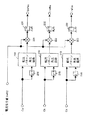
先ず本発明に係るモータ駆動制御装置20を、5相ブラシレスモータについて図1に示して説明する。モータ駆動制御装置20は制御回路21、FETゲート駆動回路22、モータ駆動回路23、電流検出回路24及びロータ位置検出回路25で構成されている。制御回路21は例えばマイクロコンピュータで構成され、定電圧源26から一定電圧が供給される。制御回路21には外部回路27から電流指令Irefが入力され、電流検出回路24からモータ電流検出値I、ロータ位置検出回路25からロータ位置信号Sa-e(=Sa,・・・・,Se)がそれぞれ入力される。制御回路21は、これらの入力信号に基づいて、モータ駆動回路23からブラシレスモータ1のコイル回路12に供給される駆動電流を制御する。
First, a motor
ここで、電動パワーステアリング装置の駆動源として5相ブラシレスモータ1を用いる場合、外部回路27は、自動車の変速機の出力軸回転数に応じたパルス信号を発生する車速センサの出力から求められる車速検出値Vと、ステアリングホイールの入力軸に加えられた操蛇トルクを検出するトルクセンサの出力から求められるトルクの方向を含む検出値Tとから、所定の特性線図を参照して対応するモータ電流値を検索し、これを電流指令Irefとして出力するように構成される。
Here, when the five-
モータ駆動回路23は、電源供給側(上段側)に5個、アース側(下段側)に5個の合計10個のトランジスタ(電界効果トランジスタFET)Ta1〜Te1,Ta2〜Te2で構成されている。これら10個のトランジスタTa1〜Te1,Ta2〜Te2は、上段側と下段側とで対応するトランジスタが直列接続され、これら直列接続のトランジスタ対(Ta1−Ta2,Tb1−Tb2,Tc1−Tc2,Td1−Td2,Te1−Te2)の各々の上段側端子は制御回路21に、下段側端子は電流検出回路24にそれぞれ接続されると共に、各トランジスタ対の接続部は、各励磁コイル6a〜6eの外端(スター結線の中心側とは逆側)と接続されている。そして、トランジスタTa1〜Te2の各々のゲート電圧は、ロータ位置検出回路25からの検出信号Sa-eに基づいて制御回路21により制御される。
The
モータ駆動回路23から各励磁コイル6a〜6eへの励磁電流の方向及び大きさは、基本的には従来と同様に図8に示すようになり、各トランジスタTa1〜Te2のオン/オフのタイミングは、下記の表1のゲート信号(上段)Ga1〜Ge1及びゲート信号(下段)Ga2〜Ge2に示すようになる。なお、表1では、各トランジスタTa1〜Te2をオン/オフするゲート信号Ga1〜Ge2を、それぞれ“1”,“0”で表わしている。
The direction and magnitude of the excitation current from the

以上の操作を繰返し行うと、表1に示すタイミングで各トランジスタが駆動され、図8に示すように電気角で36度毎に順次1相ずつ励磁コイルを切替え、1つの相を電気角で144度の間励磁する。これにより、ステータに発生するN極又はS極が順次移動し、ロータが連続回転する。FETゲート駆動回路22は、制御回路21から出力されたゲート駆動信号G1-10に基づき、指定されたトランジスタのゲート端子に所定の電圧供給を行う。
When the above operation is repeated, each transistor is driven at the timing shown in Table 1. As shown in FIG. 8, the excitation coil is sequentially switched by one phase every 36 degrees in electrical angle as shown in FIG. Energize for degrees. Thereby, the N pole or S pole generated in the stator sequentially moves, and the rotor continuously rotates. The FET
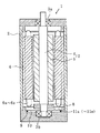
一方、モータ駆動制御装置20が駆動制御するブラシレスモータの一例(5相ブラシレスモータ1)は図2に示すようになっており、この5相ブラシレスモータ1は円筒形のハウジング2と、このハウジング2の軸心に沿って配設され、軸受3a,3bにより回転自在に支持された回転軸4と、この回転軸4に固定されたモータ駆動用の永久磁石5と、この永久磁石5を包囲するようにハウジング2の内周面に固定され且つ5相の励磁コイル6a,6b,6c,6d及び6eが巻き付けられたステータ6とを具備し、回転軸4及び永久磁石5によってロータ7を構成している。
On the other hand, an example of a brushless motor (5-phase brushless motor 1) driven and controlled by the motor
ロータ7の回転軸4の一端部の近傍には位相検出用のリング状の永久磁石8が固定され、この永久磁石8は周方向に等間隔で交互にS極とN極に着磁されている。また、ロータ7の永久磁石5も、S極及びN極が周方向に交互に等問隔で着磁されている。ハウジング2内の軸受3bが配設された側の端面には、ステー9を介してリング状の薄板から成る支持基板10が、その内側の絶縁部分が永久磁石8に対向するように配設されている。この支持基板10の永久磁石8側の面には、永久磁石8に対向するように例えばホール素子から成る位相検出素子(ホールセンサ)11が固定されている。なお、位相検出素子11は、実際には励磁コイル6a〜6eの駆動タイミングに対応して周方向に適宜離間して5個(11a〜11e)設けられているが、図2はそのうちの1つのみを示している。
A ring-shaped
上記位相検出素子11a〜11eは、各々に対向する永久磁石8の磁極が、N極の場合には位置検出信号として“H”のセンサ信号を、S極の場合には“L”のセンサ信号をそれぞれ出力する。これら各位相検出素子11a〜11eの出力は、各素子に対向する永久磁石8の磁極によって変化することを利用してロータ7の回転位置を検知できる。その回転位置に応じて、モータ駆動制御装置20が5相の励磁コイル6a〜6eに対して4相同時に通電しながら、通電する励磁コイルを1相ずつ順次切替える4相励磁方式により、ロータ7を回転駆動するようになっている。
The phase detection elements 11a to 11e have an "H" sensor signal as a position detection signal when the magnetic poles of the
また、5相の励磁コイル6a〜6eは、ロータ7の外周面を電気角で72度ずつ離隔して取り囲むように配設され、図1に示すようにY字型にスター結線されて、このモータのコイル回路12を構成している。なお、4相励磁方式では、モータ電流は4つの相に流れることになるが、電流はコイル抵抗に反比例するので、各相にバランスよく電流を流すために各励磁コイル6a〜6eのコイル抵抗は全て等しくなるように形成されている。また、ステータ6は、例えば図示しないステータコア内周面に等間隔に30個のスロットを有すると共に、これらスロット間に同数の凸部を有し、そのうち5個の凸部を1組として、各組に各励磁コイル6a〜6eを巻き付けるように構成されている。各励磁コイル6a〜6eの一端はまとめて結線され、他端はモータ駆動制御装置20に接続されている。
Further, the five-phase
本発明は、モータ駆動制御装置20内の制御回路21に設けた転流パターン発生部で転流時に所定条件に従った転流パターン1〜4(図8参照)を発生し、各相の電流指令値Irefas,Irefbs,Irefcsとしてブラシレスモータ1に与えるようになっており、図3にその構成例を示す。なお、図1のブラシレスモータ1は5相となっているが、転流については3相で説明する。
The present invention generates
本発明では、先ず正弦波波形を元にした転流時の電流指令値を定義する。この際、各相の電流指令値が正か負か、若しくは0であるかは、モータの位置により決められる。例えば非転流の時、正負又は0の電流指令値は次のように計算される。
1×210→Ireft2×(1×210)
→Iret2×(1×210)/210→・・正相の電流指令値
0×210→Ireft2×(0×210)
→Iret2×(0×210)/210→・・ゼロ相の電流指令値
−1×210→Ireft2×(−1×210)
→Iret2×(−1×210)/210→・・負相の電流指令値
即ち、転流でない場合、3相の電流指令値はIreft2,0,−Ireft2である。
In the present invention, first, a current command value at the time of commutation based on a sine wave waveform is defined. At this time, whether the current command value of each phase is positive, negative, or 0 is determined by the position of the motor. For example, when there is no commutation, a positive / negative or zero current command value is calculated as follows.
1 × 2 10 → Ireft2 × (1 × 2 10 )
→ Iret2 × (1 × 2 10 ) / 2 10 → ・ Normal phase current command value
0 × 2 10 → Ireft2 × (0 × 2 10 )
→ Iret2 × (0 × 2 10 ) / 2 10 → ・ Zero phase current command value
−1 × 2 10 → Ireft2 × (−1 × 2 10 )
→ Iret2 × (-1 × 2 10 ) / 2 10 → ・ ・ Current command value of negative phase
That is, when it is not commutation, the current command value of the three phases is Ireft2, 0, −Ireft2.
転流の場合、計算方法は非転流の場合と同一である。ただし、乗算の値は1,0,−1ではなく、経過時間により正弦波波形の値と乗算する。ここでは12ポイントの例を示す。転流がゼロ相から正相への転流だとすると、12×サンプリング時間を経過すると、乗算の値は0から1まで変化し、その間の値は0,0.017037、・・・、0.98296,1となる。電流指令値の計算は次のようにする。
転流前 ia=[Ireft2×(0×210)]/210
ステップ1 ia=[Ireft2×(0.01737×210)]/210
・
・
・
ステップ11 ia=[Ireft2×(0.98296×210)]/210
ステップ12 ia=[Ireft2×(1×210)]/210
転流パターン発生部には、転流を表わすパラメータとしてのCa,Cb,Ccがそれぞれ転流パターン発生回路211,212,213に入力されると共に、それぞれディジタル制御におけるZ−1回路214,215,216(1サンプリング遅れ)を経て転流パターン発生回路211,212,213に入力される。また、電流指令値Ireft2は乗算回路に入力され、それぞれ転流パターン発生回路211,212,213の出力と乗算され、各乗算結果が係数回路(2−10)231,232,233を経て電流指令値Irefas,Irefbs,Irefcsとして出力される。
For commutation, the calculation method is the same as for noncommutation. However, the value of multiplication is not 1, 0, -1, but is multiplied by the value of the sine wave waveform by the elapsed time. Here, an example of 12 points is shown. If the commutation is commutation from the zero phase to the positive phase, after 12 × sampling time has elapsed, the value of multiplication changes from 0 to 1, and the value therebetween is 0,0.017037,..., 0.98296. , 1 The current command value is calculated as follows.
Before commutation ia = [Ireft2 × (0 × 2 10 )] / 2 10
・
・
・
Step 11 ia = [Iref2 × (0.98296 × 2 10 )] / 2 10
In the commutation pattern generation unit, Ca, Cb, and Cc as parameters representing commutation are input to the commutation
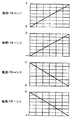
転流パターン発生回路211,212,213は図4に示すような4種類の転流パターンを発生するようになっている。即ち、転流パターン1は“0→1”の正弦波波形であり、転流パターン2は“−1→0”の正弦波波形であり、転流パターン3は“1→0”の正弦波波形であり、転流パターン4は“0→−1”の正弦波波形である。転流パターン1〜4は擬似正弦波波形であっても良い。転流パターン発生回路211,212,213のそれぞれが、所定の入力の条件に従って転流パターン1〜4を生成して出力する。
The commutation
なお、転流パラメータCa,Cb,Ccは位相検出素子(ホールセンサ)に基づいて生成され、表2に示すような関係で生成出力される。 The commutation parameters Ca, Cb, and Cc are generated based on the phase detection element (Hall sensor), and are generated and output in the relationship shown in Table 2.
Ca(k)=1のとき、 転流パターン1を発生
Ca(k)=0でCa(k−1)=−1のとき 転流パターン2を発生
Ca(k)=0でCa(k−1)=1のとき 転流パターン3を発生
Ca(k)=−1のとき 転流パターン4を発生
転流パターン発生回路212及び213についても同様であり、Cb(k)及びCb(k−1)、Cc(k)及びCc(k−1)に基づいてそれぞれ転流パターン1〜4を発生する。転流パターン発生回路211の構成は、転流パラメータCa(k−1)と1サンプリング(Z−1)遅れた転流パラメータCa(k)を比較手段で比較し、両者が同じであれば非転流状態と判断し、ある瞬間で両者の出力が相違すれば転流の開始と判断し、その条件に従って予め登録されている転流パターンデータを読出して出力する。転流パターン発生回路212及び213についても同様である。
When Ca (k) = 1,
The same applies to the commutation
転流時間を例えば6ミリ秒としたとき、転流パターン1〜4は下記表3の数値で演算出力される。ここにおいて、転流パターン1〜4の最大値は“1”であり、最小値は“−1”であり、その間は小数となるが、小数はソフト演算できない。このため、精度を考慮して、210を乗算して整数になるようにしている。そのため、転流パターンのグラフ(図4)では“−1、−0.98296、・・・、0、・・・、0.98296、1”となっている数値をソフトでは事前計算し、“−1024、−1007、・・・、0、・・・、1007、1024”としている。このように事前に210で拡大しているので、出力では事前の210因数を排除するため、2−10を係数として乗算している。
When the commutation time is, for example, 6 milliseconds, the
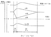
転流パターン発生回路211〜213から出力された転流パターンは、それぞれ乗算回路221〜223で乗算され、係数回路231〜233を経て電流指令値Irefas,Irefbs,Irefcsとして出力される。転流波形を図示すると一般的には図5(C)のようになるが、本発明では、1相では図5(A)のようになり、3相では図5(B)のようになる。
The commutation patterns output from the commutation
本発明では、転流時の転流パターンを生成する転流パターン発生部を設け、転流パターンに基づいて、転流時の電流指令値を予め定められて数値、つまり、転流パターンの2相の和が1又は−1となる数値の組とし、転流パターンと電流指令値とを乗じてブラシレスモータ各相への電流指令値を算出している。例えば転流ポイント12の場合、転流時間は12×サンプリング時間となり、その間に1/4周期の正弦波波形で12等分すると、図4及び表3で示すように
[0.017037,0.066987,0.14645,0.25,0.37059,0.5,0.62941,0.75,0.85355,0.93301,0.98296,1]
=[17,69,150,256,379,512,645,768,874,955,1007,1024]
となる。そして、転流パターンの2相の和が1(整数では1024)又は−1(整数では−1024)となる数値の組とする。転流中でも3相電流の和は0であるので、転流相の電流は変化しても、非転流相の電流を変化しないようにするため、転流相電流の和は転流の間、いつでも非転流相の大きさと同一で、方向が逆でなければならない。なお、正弦波波形に限らず、転流パターンの2相の和が1又は−1となれば、トルクリップルを発生させることなく滑らかに転流することができる。
In the present invention, a commutation pattern generation unit that generates a commutation pattern at the time of commutation is provided, and a current command value at the time of commutation is determined in advance based on the commutation pattern, that is, 2 of the commutation pattern. The current command value for each phase of the brushless motor is calculated by multiplying the commutation pattern and the current command value by using a set of numerical values where the sum of the phases is 1 or -1. For example, in the case of the
[0.017037, 0.066987, 0.14645, 0.25, 0.37059, 0.5, 0.62941, 0.75, 0.85355, 0.93301, 0.98296, 1]
= [17, 69, 150, 256, 379, 512, 645, 768, 874, 955, 1007, 1024]
It becomes. And it is set as the numerical value set from which the sum of the two phases of a commutation pattern becomes 1 (1024 in an integer) or -1 (-1024 in an integer). Since the sum of the three-phase currents is 0 even during commutation, the sum of the commutation phase currents does not change during commutation so that the current of the non-commutation phase does not change even if the current of the commutation phase changes. It must always be the same size as the non-commutated phase and the direction reversed. In addition, if it is not restricted to a sine wave waveform and the sum of the two phases of a commutation pattern will be set to 1 or -1, it can commutate smoothly, without generating a torque ripple.
図6は転流パターンの2相の和が1又は−1となる直線波形の例を示しており、転流パターン1は“0→1”の直線波形であり、転流パターン2は“−1→0”の直線波形であり、転流パターン3は“1→0”の直線波形であり、転流パターン4は“0→−1”の直線波形である。また、図7は転流パターンの2相の和が1又は−1となるべき乗関数(1−e−t/T)波形の例を示しており、転流パターン1は“0→1”のべき乗関数波形であり、転流パターン2は“−1→0”のべき乗関数波形であり、転流パターン3は“1→0”のべき乗関数波形であり、転流パターン4は“0→−1”のべき乗関数波形である。このような転流パターン波形を用いることも可能である。
FIG. 6 shows an example of a linear waveform in which the sum of the two phases of the commutation pattern is 1 or −1. The
上述の実施例では3相のブラシレスモータに本発明を適用した例を示したが、本発明はこれに限定されるものではなく、他の複数の励磁相(例えば5相)のブラシレスモータについても本発明を適用することができる。また、上述の実施例では、図8に示すように、上段側のトランジスタ(例えばTa1)と下段側のトランジスタ(例えばTa2)とが同じPMWデューティで駆動される例を示したが、本発明はこれに限定されるものではなく、上段側のトランジスタ(例えばTa1)と下段側のトランジスタ(例えばTa2)とが異なるPMWデューティで駆動されるものについても本発明を適用することができる。 In the above-described embodiment, an example in which the present invention is applied to a three-phase brushless motor has been described. However, the present invention is not limited to this, and the brushless motor of other plural excitation phases (for example, five phases) can also be used. The present invention can be applied. In the above-described embodiment, as shown in FIG. 8, the example in which the upper transistor (for example, Ta1) and the lower transistor (for example, Ta2) are driven with the same PMW duty is shown. The present invention is not limited to this, and the present invention can also be applied to the case where the upper transistor (for example, Ta1) and the lower transistor (for example, Ta2) are driven with different PMW duties.
本発明によれば、ブラシレスモータに対する転流時の振動や騒音の発生を抑制するため、転流時に正弦波波形(若しくは擬似正弦波波形)で電流指令値を与えると共に、転流パターンの2相の和が1(整数では1024)又は−1(整数では−1024)となる数値のペアで与えると共に、転流パターンと電流指令値とを乗算してブラシレスモータ各相への電流指令値を算出するようにしている。これにより、ブラシレスモータを矩形波で制御する場合でも、低振動及び低騒音を実現することができ、自動車や車両の高性能電動パワーステアリングに適用することが可能である。 According to the present invention, in order to suppress generation of vibration and noise during commutation for a brushless motor, a current command value is given as a sine wave waveform (or pseudo sine wave waveform) during commutation, and two phases of the commutation pattern are provided. Is given as a pair of numerical values whose sum is 1 (1024 for integer) or -1 (-1024 for integer), and the commutation pattern and current command value are multiplied to calculate the current command value for each phase of the brushless motor Like to do. As a result, even when the brushless motor is controlled by a rectangular wave, low vibration and low noise can be realized, and it can be applied to high performance electric power steering of automobiles and vehicles.
1 ブラシレスモータ
2 ハウジング
3a,3b 軸受
4 回転軸
5 永久磁石
6 ステータ
7 ロータ
11 位相検出素子(ホールセンサ)
20 モータ駆動制御装置
21 制御回路
22 FETゲート駆動回路
23 モータ駆動回路
24 電流検出回路
25 ロータ位置検出回路
27 外部回路
211〜213 転流パターン発生回路
221〜223 乗算回路
231〜233 係数回路
DESCRIPTION OF
DESCRIPTION OF
Claims (3)
The brushless motor drive control device according to claim 2, wherein the commutation pattern has a sinusoidal waveform.
Priority Applications (1)
| Application Number | Priority Date | Filing Date | Title |
|---|---|---|---|
| JP2004011416A JP2005210764A (en) | 2004-01-20 | 2004-01-20 | Drive controller of brushless motor |
Applications Claiming Priority (1)
| Application Number | Priority Date | Filing Date | Title |
|---|---|---|---|
| JP2004011416A JP2005210764A (en) | 2004-01-20 | 2004-01-20 | Drive controller of brushless motor |
Publications (2)
| Publication Number | Publication Date |
|---|---|
| JP2005210764A true JP2005210764A (en) | 2005-08-04 |
| JP2005210764A5 JP2005210764A5 (en) | 2007-03-01 |
Family
ID=34898109
Family Applications (1)
| Application Number | Title | Priority Date | Filing Date |
|---|---|---|---|
| JP2004011416A Pending JP2005210764A (en) | 2004-01-20 | 2004-01-20 | Drive controller of brushless motor |
Country Status (1)
| Country | Link |
|---|---|
| JP (1) | JP2005210764A (en) |
Cited By (1)
| Publication number | Priority date | Publication date | Assignee | Title |
|---|---|---|---|---|
| CN113954955A (en) * | 2021-10-14 | 2022-01-21 | 济南科亚电子科技有限公司 | Implementation method of electric steering wheel motor drive controller |
-
2004
- 2004-01-20 JP JP2004011416A patent/JP2005210764A/en active Pending
Cited By (1)
| Publication number | Priority date | Publication date | Assignee | Title |
|---|---|---|---|---|
| CN113954955A (en) * | 2021-10-14 | 2022-01-21 | 济南科亚电子科技有限公司 | Implementation method of electric steering wheel motor drive controller |
Similar Documents
| Publication | Publication Date | Title |
|---|---|---|
| US6838848B2 (en) | Brushless motor control method | |
| JP3690341B2 (en) | Brushless DC motor driving method and apparatus | |
| US6400116B1 (en) | Motor drive control apparatus | |
| JP2006166574A (en) | Inverter device | |
| US6469463B2 (en) | Brushless motor and driving control device therefor | |
| US6934468B2 (en) | Brushless DC motor and circuit for controlling the same | |
| JP2014075931A (en) | Drive control device for stepping motor | |
| JP2014014197A (en) | Single-phase brushless motor | |
| JP2000175478A (en) | Device and method for driving polyphase motor | |
| US6969962B2 (en) | DC motor drive circuit | |
| JP3298508B2 (en) | Motor drive control device | |
| JP2005210764A (en) | Drive controller of brushless motor | |
| JP2008029115A (en) | Single-phase position sensorless permanent magnet motor controller | |
| KR100710515B1 (en) | Motor drive control apparatus | |
| JP4779233B2 (en) | Brushless motor drive control device | |
| JP4052442B2 (en) | MOTOR CONTROL DEVICE, MOTOR, ELECTRIC DEVICE, AND MOTOR CONTROL METHOD | |
| JPH06121588A (en) | Drive system for variable reluctance motor | |
| JPH08242600A (en) | Current controller for hybrid excitation type permanent magnet motor | |
| JP2004015968A (en) | Brushless electric motor drive control device | |
| JP2007252136A (en) | Drive unit of brushless motor | |
| JP4312115B2 (en) | Motor drive device | |
| JP2006353096A (en) | Brushless electric motor and its drive control device | |
| JP2006158166A (en) | Sensorless synchronous motor, and its driving method and device | |
| Niranjan et al. | Speed Control of BLDC Motor Using Microprocessor | |
| JP2008029116A (en) | Single-phase permanent magnet motor controller, fan and pump |
Legal Events
| Date | Code | Title | Description |
|---|---|---|---|
| A711 | Notification of change in applicant |
Free format text: JAPANESE INTERMEDIATE CODE: A711 Effective date: 20050711 |
|
| A521 | Written amendment |
Free format text: JAPANESE INTERMEDIATE CODE: A523 Effective date: 20070117 |
|
| A621 | Written request for application examination |
Free format text: JAPANESE INTERMEDIATE CODE: A621 Effective date: 20070117 |
|
| A131 | Notification of reasons for refusal |
Free format text: JAPANESE INTERMEDIATE CODE: A131 Effective date: 20091006 |
|
| A977 | Report on retrieval |
Free format text: JAPANESE INTERMEDIATE CODE: A971007 Effective date: 20091008 |
|
| A02 | Decision of refusal |
Free format text: JAPANESE INTERMEDIATE CODE: A02 Effective date: 20100223 |