JP2005206409A - Method for growing group iii nitride crystal, group iii nitride crystal, semiconductor device, and system - Google Patents
Method for growing group iii nitride crystal, group iii nitride crystal, semiconductor device, and system Download PDFInfo
- Publication number
- JP2005206409A JP2005206409A JP2004013562A JP2004013562A JP2005206409A JP 2005206409 A JP2005206409 A JP 2005206409A JP 2004013562 A JP2004013562 A JP 2004013562A JP 2004013562 A JP2004013562 A JP 2004013562A JP 2005206409 A JP2005206409 A JP 2005206409A
- Authority
- JP
- Japan
- Prior art keywords
- group iii
- crystal
- iii nitride
- nitride crystal
- semiconductor device
- Prior art date
- Legal status (The legal status is an assumption and is not a legal conclusion. Google has not performed a legal analysis and makes no representation as to the accuracy of the status listed.)
- Pending
Links
Images


Classifications
-
- H—ELECTRICITY
- H01—ELECTRIC ELEMENTS
- H01L—SEMICONDUCTOR DEVICES NOT COVERED BY CLASS H10
- H01L2224/00—Indexing scheme for arrangements for connecting or disconnecting semiconductor or solid-state bodies and methods related thereto as covered by H01L24/00
- H01L2224/01—Means for bonding being attached to, or being formed on, the surface to be connected, e.g. chip-to-package, die-attach, "first-level" interconnects; Manufacturing methods related thereto
- H01L2224/42—Wire connectors; Manufacturing methods related thereto
- H01L2224/47—Structure, shape, material or disposition of the wire connectors after the connecting process
- H01L2224/48—Structure, shape, material or disposition of the wire connectors after the connecting process of an individual wire connector
- H01L2224/4805—Shape
- H01L2224/4809—Loop shape
- H01L2224/48091—Arched
-
- H—ELECTRICITY
- H01—ELECTRIC ELEMENTS
- H01L—SEMICONDUCTOR DEVICES NOT COVERED BY CLASS H10
- H01L2224/00—Indexing scheme for arrangements for connecting or disconnecting semiconductor or solid-state bodies and methods related thereto as covered by H01L24/00
- H01L2224/01—Means for bonding being attached to, or being formed on, the surface to be connected, e.g. chip-to-package, die-attach, "first-level" interconnects; Manufacturing methods related thereto
- H01L2224/42—Wire connectors; Manufacturing methods related thereto
- H01L2224/47—Structure, shape, material or disposition of the wire connectors after the connecting process
- H01L2224/48—Structure, shape, material or disposition of the wire connectors after the connecting process of an individual wire connector
- H01L2224/481—Disposition
- H01L2224/48151—Connecting between a semiconductor or solid-state body and an item not being a semiconductor or solid-state body, e.g. chip-to-substrate, chip-to-passive
- H01L2224/48221—Connecting between a semiconductor or solid-state body and an item not being a semiconductor or solid-state body, e.g. chip-to-substrate, chip-to-passive the body and the item being stacked
- H01L2224/48245—Connecting between a semiconductor or solid-state body and an item not being a semiconductor or solid-state body, e.g. chip-to-substrate, chip-to-passive the body and the item being stacked the item being metallic
- H01L2224/48247—Connecting between a semiconductor or solid-state body and an item not being a semiconductor or solid-state body, e.g. chip-to-substrate, chip-to-passive the body and the item being stacked the item being metallic connecting the wire to a bond pad of the item
-
- H—ELECTRICITY
- H01—ELECTRIC ELEMENTS
- H01L—SEMICONDUCTOR DEVICES NOT COVERED BY CLASS H10
- H01L2924/00—Indexing scheme for arrangements or methods for connecting or disconnecting semiconductor or solid-state bodies as covered by H01L24/00
- H01L2924/15—Details of package parts other than the semiconductor or other solid state devices to be connected
- H01L2924/181—Encapsulation
Abstract
Description
本発明は、III族窒化物の結晶成長方法およびIII族窒化物結晶および半導体デバイスおよびシステムに関する。 The present invention relates to a group III nitride crystal growth method, a group III nitride crystal, and a semiconductor device and system.
現在、紫外,紫〜青〜緑色光源として用いられているInGaAlN系(III族窒化物)デバイスは、その殆どがサファイアあるいはSiC基板上に、MO−CVD法(有機金属化学気相成長法)やMBE法(分子線結晶成長法)等を用いた結晶成長により作製されている。サファイアやSiCを基板として用いる場合の問題点としては、III族窒化物との熱膨張係数差や格子定数差が大きいことに起因する結晶欠陥が多くなることが挙げられ、このために、デバイス特性が悪かったり(例えば発光デバイスの寿命を長くすることが困難であったり)、動作電力が大きくなったりするという問題が生じる。 At present, most of InGaAlN-based (group III nitride) devices used as ultraviolet, purple-blue-green light sources are formed on a sapphire or SiC substrate by MO-CVD (metal organic chemical vapor deposition), It is produced by crystal growth using the MBE method (molecular beam crystal growth method) or the like. Problems when using sapphire or SiC as a substrate include increased crystal defects due to large differences in thermal expansion coefficients and lattice constants from group III nitrides. Are bad (for example, it is difficult to extend the lifetime of the light-emitting device) or the operating power increases.
更に、サファイア基板の場合には絶縁性であるために、従来の発光デバイスのように基板側からの電極取り出しが不可能であり、結晶成長した窒化物半導体表面側からの電極取り出しが必要となる。その結果、デバイス面積が大きくなり、高コストにつながるという問題点がある。また、サファイア基板上に作製したIII族窒化物半導体デバイスは劈開によるチップ分離が困難であり、レーザダイオード(LD)で必要とされる共振器端面を劈開で得ることが容易ではない。このため、現在はドライエッチングによる共振器端面形成や、あるいはサファイア基板を100μm以下の厚さまで研磨した後に、劈開に近い形での共振器端面形成を行っている。この場合にも、従来のLDのような共振器端面とチップ分離を単一工程で、容易に行うことが不可能であり、工程の複雑化ひいてはコスト高につながる。 Furthermore, in the case of a sapphire substrate, since it is insulative, it is impossible to take out the electrode from the substrate side as in the conventional light emitting device, and it is necessary to take out the electrode from the nitride semiconductor surface side where the crystal has grown. . As a result, there is a problem that the device area becomes large, leading to high costs. In addition, a group III nitride semiconductor device fabricated on a sapphire substrate is difficult to be separated by cleavage, and it is not easy to obtain a resonator end face required for a laser diode (LD) by cleavage. For this reason, at present, resonator end faces are formed by dry etching, or resonator end faces are formed in a form close to cleavage after polishing the sapphire substrate to a thickness of 100 μm or less. Also in this case, it is impossible to easily separate the resonator end face from the conventional LD and the chip in a single process, resulting in a complicated process and an increase in cost.
これらの問題を解決するために、サファイア基板上でのIII族窒化物半導体膜の選択横方向成長やその他の工夫を行うことで、結晶欠陥を低減させることが提案されている。この手法では、サファイア基板上にGaN膜を選択横方向成長しない場合に比較して、結晶欠陥を低減させることが可能となるが、サファイア基板を用いることによる、絶縁性と劈開に関する前述の問題は依然として残っている。更には、工程が複雑化すること、及び、サファイア基板とGaN薄膜という異種材料の組み合わせに伴う基板の反りという問題が生じ、これらは高コスト化につながっている。 In order to solve these problems, it has been proposed to reduce crystal defects by performing selective lateral growth of the group III nitride semiconductor film on the sapphire substrate and other devices. Although this method makes it possible to reduce crystal defects compared to the case where a GaN film is not selectively grown in a lateral direction on a sapphire substrate, the above-mentioned problems related to insulation and cleavage by using a sapphire substrate Still remains. Furthermore, the process is complicated, and problems of warping of the substrate due to the combination of different materials such as a sapphire substrate and a GaN thin film arise, which leads to higher costs.
こうした問題を解決するためには、基板として、基板上に結晶成長する材料と同一であるGaN基板の実現が最も望ましい。そのため、気相成長,融液成長等により、バルクGaNの結晶成長の研究がなされている。しかし、未だ高品質で且つ実用的な大きさを有するGaN基板は実現されていない。 In order to solve these problems, it is most desirable to realize a GaN substrate that is the same as the material for crystal growth on the substrate. Therefore, research on crystal growth of bulk GaN has been made by vapor phase growth, melt growth and the like. However, a high-quality and practical size GaN substrate has not yet been realized.
GaN基板を実現する一つの手法として、非特許文献1(第一の従来技術)には、Naをフラックスとして用いたGaN結晶成長方法が提案されている。この方法は、アジ化ナトリウム(NaN3)と金属Gaを原料として、ステンレス製の反応容器(容器内寸法;内径=7.5mm、長さ=100mm)に窒素雰囲気で封入し、その反応容器を600〜800℃の温度で24〜100時間保持することにより、GaN結晶を成長させるものである。 As one method for realizing a GaN substrate, Non-Patent Document 1 (first prior art) proposes a GaN crystal growth method using Na as a flux. In this method, sodium azide (NaN 3 ) and metal Ga are used as raw materials, and sealed in a stainless steel reaction vessel (inner vessel dimensions; inner diameter = 7.5 mm, length = 100 mm) in a nitrogen atmosphere. A GaN crystal is grown by holding at a temperature of 600 to 800 ° C. for 24 to 100 hours.
この第一の従来技術は、600〜800℃と比較的低温での結晶成長が可能であり、容器内圧力も高々100kg/cm2程度と比較的圧力が低く、実用的な成長条件であることが特徴である。しかし、この方法の問題点としては、得られる結晶の大きさが1mmに満たない程度に小さい点である。 This first prior art is capable of crystal growth at a relatively low temperature of 600 to 800 ° C., and the pressure in the vessel is relatively low at about 100 kg / cm 2, which is a practical growth condition. Is a feature. However, the problem with this method is that the crystal size obtained is small enough to be less than 1 mm.
すなわち、第一の従来技術では、反応容器が完全に閉じた系であり、外部から原料を補充する事ができない。そのため、結晶成長中に原料が枯渇し、結晶成長が停止するので、得られる結晶の大きさは1mm程度と小さい。この程度の大きさではデバイスを実用化するには小さすぎる。 That is, in the first prior art, the reaction vessel is a completely closed system, and the raw material cannot be replenished from the outside. Therefore, the raw material is depleted during the crystal growth and the crystal growth stops, so that the size of the obtained crystal is as small as about 1 mm. This size is too small for practical use of the device.
この第一の従来技術の問題を解決するために、特許文献1,特許文献2に示されているような方法が提案されている。 In order to solve the problem of the first prior art, methods as shown in Patent Document 1 and Patent Document 2 have been proposed.
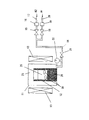
すなわち、特許文献1(第二の従来技術)には、III族窒化物結晶の大きさを大きくするために、III族窒化物結晶の結晶成長時に、III族金属を追加補充する方法が示されている。より具体的に、この方法では、図14に示すように、反応容器101内に成長容器102とIII族金属供給管103を設け、III族金属供給管103に外部から圧力をかけ、フラックスの収容された反応容器102にIII族金属104を追加補給するようにしている。
That is, Patent Document 1 (second prior art) shows a method of additionally supplementing a Group III metal during the growth of a Group III nitride crystal in order to increase the size of the Group III nitride crystal. ing. More specifically, in this method, as shown in FIG. 14, a
また、特許文献2(第三の従来技術)には、フラックス(Na)とIII族金属(Ga)の混合融液が収容された融液供給管に外部から圧力をかけ、フラックスの収容された成長容器に混合融液を追加補給する方法と、成長容器内にフラックス(Na)とIII族金属(Ga)の金属間化合物を入れ、それを部分的に融解してIII族金属を追加補給する方法が示されている。
上述した第二,第三の従来技術では、原料の追加補給を結晶成長の途中で行うので、大型のIII族窒化物結晶を作製する事が可能である。 In the second and third prior arts described above, additional replenishment of the raw material is performed during crystal growth, so that a large group III nitride crystal can be produced.
しかしながら、当業者間には、第二,第三の従来技術よりもさらに低コストで、実用的な大型,大面積のIII族窒化物の基板結晶を作製できる方法が望まれている。 However, there is a demand for a person skilled in the art to manufacture a practical large-sized, large-area group III nitride substrate crystal at a lower cost than the second and third prior arts.
本発明は、従来よりも低コストで、実用的な大きさの大型,大面積の高品質なIII族窒化物結晶を作製することの可能なIII族窒化物の結晶成長方法及びIII族窒化物結晶及び半導体デバイス及びシステムを提供することを目的としている。 INDUSTRIAL APPLICABILITY The present invention is a group III nitride crystal growth method and a group III nitride capable of producing a large-sized, large-area, high-quality group III nitride crystal having a practical size at a lower cost than before. It is an object to provide crystal and semiconductor devices and systems.
上記目的を達成するために、請求項1記載の発明は、少なくともアルカリ金属とIII族金属と窒素が溶解した融液からIII族窒化物結晶を成長させる結晶成長方法において、前記融液に、III族窒化物結晶のc軸方向の成長速度とc軸に垂直な方向の成長速度との比率を制御する物質を含ませることを特徴としている。 To achieve the above object, the invention described in claim 1 is a crystal growth method for growing a group III nitride crystal from a melt in which at least an alkali metal, a group III metal, and nitrogen are dissolved. It is characterized by containing a substance that controls the ratio of the growth rate in the c-axis direction of the group nitride crystal to the growth rate in the direction perpendicular to the c-axis.
また、請求項2記載の発明は、請求項1記載の結晶成長方法において、前記融液に、III族窒化物結晶のc軸に垂直な方向の成長速度をc軸方向の成長速度よりも速くする物質を含ませて、III族窒化物結晶を成長させることを特徴としている。 The invention according to claim 2 is the crystal growth method according to claim 1, wherein the growth rate of the group III nitride crystal in the direction perpendicular to the c-axis is higher than the growth rate in the c-axis direction. It is characterized in that a group III nitride crystal is grown by including the material to be treated.
また、請求項3記載の発明は、請求項1または請求項2記載の結晶成長方法において、種結晶(例えば、板状の種結晶)を用い、種結晶(例えば、板状の種結晶)の主面に平行な方向の成長速度が種結晶の主面に垂直な方向の成長速度よりも速い速度で、種結晶(例えば、板状の種結晶)の主面にIII族窒化物結晶を成長させることを特徴としている。 The invention according to claim 3 is the crystal growth method according to claim 1 or 2, wherein a seed crystal (for example, a plate-shaped seed crystal) is used, and a seed crystal (for example, a plate-shaped seed crystal) is used. A group III nitride crystal is grown on the main surface of the seed crystal (for example, a plate-shaped seed crystal) at a growth rate in the direction parallel to the main surface that is faster than the growth rate in the direction perpendicular to the main surface of the seed crystal. It is characterized by letting.
また、請求項4記載の発明は、請求項3記載の結晶成長方法において、c面を主面とするIII族窒化物結晶(例えば、板状のIII族窒化物結晶)を種結晶として、該種結晶のc面にIII族窒化物結晶を成長させることを特徴としている。 The invention described in claim 4 is the crystal growth method according to claim 3, wherein a group III nitride crystal having a c-plane as a main surface (for example, a plate-like group III nitride crystal) is used as a seed crystal. A group III nitride crystal is grown on the c-plane of the seed crystal.
また、請求項5記載の発明は、少なくともアルカリ金属とIII族金属と窒素が溶解した融液からIII族窒化物結晶を成長させる結晶成長方法において、前記融液に、リチウム(Li)を含ませることを特徴としている。 The invention according to claim 5 is a crystal growth method for growing a group III nitride crystal from a melt in which at least an alkali metal, a group III metal, and nitrogen are dissolved, and lithium (Li) is included in the melt. It is characterized by that.
また、請求項6記載の発明は、請求項1乃至請求項5のいずれか一項に記載の結晶成長方法で結晶成長させたIII族窒化物結晶である。 A sixth aspect of the present invention is a group III nitride crystal grown by the crystal growth method according to any one of the first to fifth aspects.
また、請求項7記載の発明は、請求項6記載のIII族窒化物結晶を用いたことを特徴とする半導体デバイスである。 The invention described in claim 7 is a semiconductor device using the group III nitride crystal described in claim 6.
また、請求項8記載の発明は、請求項7記載の半導体デバイスにおいて、該半導体デバイスは、請求項6記載のIII族窒化物結晶上に積層した半導体積層構造を有する発光素子であることを特徴としている。 The invention according to claim 8 is the semiconductor device according to claim 7, wherein the semiconductor device is a light emitting element having a semiconductor multilayer structure laminated on the group III nitride crystal according to claim 6. It is said.
また、請求項9記載の発明は、請求項7記載の半導体デバイスにおいて、該半導体デバイスは、請求項6記載のIII族窒化物結晶を用いて形成された受光素子であることを特徴としている。 The invention according to claim 9 is the semiconductor device according to claim 7, wherein the semiconductor device is a light receiving element formed using the group III nitride crystal according to claim 6.
また、請求項10記載の発明は、請求項7記載の半導体デバイスにおいて、該半導体デバイスは、請求項6記載のIII族窒化物結晶を用いて形成された電子デバイスであることを特徴としている。 According to a tenth aspect of the present invention, there is provided the semiconductor device according to the seventh aspect, wherein the semiconductor device is an electronic device formed using the group III nitride crystal according to the sixth aspect.
また、請求項11記載の発明は、請求項7乃至請求項10のいずれか一項に記載の半導体デバイスを具備したことを特徴とするシステムである。 An eleventh aspect of the invention is a system including the semiconductor device according to any one of the seventh to tenth aspects.
請求項1記載の発明によれば、少なくともアルカリ金属とIII族金属と窒素が溶解した融液からIII族窒化物結晶を成長させる結晶成長方法において、前記融液に、III族窒化物結晶のc軸方向の成長速度とc軸に垂直な方向の成長速度との比率を制御する物質を含ませるので、結晶の形態を制御することができる。 According to the first aspect of the present invention, in the crystal growth method of growing a group III nitride crystal from a melt in which at least an alkali metal, a group III metal, and nitrogen are dissolved, the melt includes c of the group III nitride crystal. Since the substance for controlling the ratio between the growth rate in the axial direction and the growth rate in the direction perpendicular to the c-axis is included, the morphology of the crystal can be controlled.
また、請求項2記載の発明によれば、請求項1記載の結晶成長方法において、前記融液に、III族窒化物結晶のc軸に垂直な方向の成長速度をc軸方向の成長速度よりも速くする物質を含ませて、III族窒化物結晶を成長させるので、結晶の形態を板状に制御することができる。そして、板状に制御できることから、そのまま基板として使えて、基板作製の低コスト化が可能となる。 According to a second aspect of the present invention, in the crystal growth method according to the first aspect, in the melt, a growth rate in the direction perpendicular to the c-axis of the group III nitride crystal is determined from a growth rate in the c-axis direction. In addition, since the group III nitride crystal is grown by including a material that accelerates the crystal, the form of the crystal can be controlled in a plate shape. And since it can control to plate shape, it can use as it is as a board | substrate and the cost reduction of board | substrate manufacture is attained.
また、請求項3記載の発明によれば、請求項1または請求項2記載の結晶成長方法において、種結晶(例えば、板状の種結晶)を用い、種結晶(例えば、板状の種結晶)の主面に平行な方向の成長速度が種結晶の主面に垂直な方向の成長速度よりも速い速度で、種結晶(例えば、板状の種結晶)の主面にIII族窒化物結晶を成長させるので、平坦な表面を主面とする結晶を成長させることができる。 According to a third aspect of the invention, in the crystal growth method of the first or second aspect, a seed crystal (for example, a plate-shaped seed crystal) is used, and a seed crystal (for example, a plate-shaped seed crystal) is used. The group III nitride crystal is formed on the main surface of the seed crystal (for example, a plate-like seed crystal) at a growth rate in a direction parallel to the main surface of Therefore, a crystal having a flat surface as a main surface can be grown.
また、請求項4記載の発明によれば、請求項3記載の結晶成長方法において、c面を主面とするIII族窒化物結晶(板状のIII族窒化物結晶)を種結晶として、該種結晶のc面にIII族窒化物結晶を成長させるので、高品質で、平坦なc面を主面とするIII族窒化物結晶を成長させることができる。 According to the invention of claim 4, in the crystal growth method of claim 3, the group III nitride crystal (plate-like group III nitride crystal) having the c-plane as the main surface is used as a seed crystal. Since the group III nitride crystal is grown on the c-plane of the seed crystal, a high-quality group III nitride crystal having a flat c-plane as the main surface can be grown.
また、請求項5記載の発明によれば、少なくともアルカリ金属とIII族金属と窒素が溶解した融液からIII族窒化物結晶を成長させる結晶成長方法において、前記融液に、リチウム(Li)を含ませることにより、リチウムは、融液中の窒素濃度を増加させるとともに、III族窒化物結晶のc軸に垂直な方向の成長速度をc軸に平行な方向の成長速度よりも大きくし、高品質な板状のIII族窒化物結晶を成長させることができる。 According to a fifth aspect of the present invention, in the crystal growth method for growing a group III nitride crystal from a melt in which at least an alkali metal, a group III metal, and nitrogen are dissolved, lithium (Li) is added to the melt. Inclusion of lithium increases the nitrogen concentration in the melt and increases the growth rate of the group III nitride crystal in the direction perpendicular to the c-axis to be higher than the growth rate in the direction parallel to the c-axis. A quality plate-like group III nitride crystal can be grown.
また、リチウムを含む融液を用いて結晶成長させたIII族窒化物結晶は、特別な不純物を混合しなくても数MΩ以上の高抵抗になる。したがって、本発明のIII族窒化物結晶を用いて、高品質の高抵抗基板を作製することができる。 In addition, a group III nitride crystal grown using a melt containing lithium has a high resistance of several MΩ or more without mixing special impurities. Therefore, a high-quality high-resistance substrate can be produced using the group III nitride crystal of the present invention.
また、請求項6記載の発明によれば、請求項1乃至請求項5のいずれか一項に記載の結晶成長方法で結晶成長させたIII族窒化物結晶であるので、高品質なIII族窒化物結晶を提供することができる。 According to the invention of claim 6, since it is a group III nitride crystal grown by the crystal growth method according to any one of claims 1 to 5, high-quality group III nitriding Physical crystals can be provided.
また、請求項7記載の発明によれば、請求項6記載のIII族窒化物結晶を用いた半導体デバイスであるので、従来よりも高性能,高信頼性の半導体デバイスを提供することができる。すなわち、本発明の半導体デバイスを構成するIII族窒化物結晶には半導体デバイスの性能に悪影響を及ぼす欠陥が少ないので、従来よりも高性能,高信頼性の半導体デバイスを提供することができる。 Further, according to the seventh aspect of the invention, since it is a semiconductor device using the group III nitride crystal according to the sixth aspect, it is possible to provide a semiconductor device with higher performance and higher reliability than the prior art. That is, since the group III nitride crystal constituting the semiconductor device of the present invention has few defects that adversely affect the performance of the semiconductor device, it is possible to provide a semiconductor device with higher performance and higher reliability than before.
また、請求項8記載の発明によれば、請求項7記載の半導体デバイスにおいて、該半導体デバイスは、請求項6記載のIII族窒化物結晶上に積層した半導体積層構造を有する発光素子であるので、該発光素子は、欠陥が少なく、高出力動作においても長寿命である。従って、従来よりも高出力で動作可能で高信頼性の発光素子を提供することができる。 According to the invention of claim 8, in the semiconductor device of claim 7, the semiconductor device is a light emitting element having a semiconductor laminated structure laminated on the group III nitride crystal of claim 6. The light emitting element has few defects and has a long life even in high output operation. Accordingly, it is possible to provide a highly reliable light-emitting element that can operate at a higher output than the conventional one.
また、請求項9の発明によれば、請求項7記載の半導体デバイスにおいて、該半導体デバイスは、請求項6記載のIII族窒化物結晶を用いて形成された受光素子であるので、受光素子を構成するIII族窒化物結晶に欠陥が少なく、暗電流が小さい。従って、従来よりもノイズレベルが低くS/N比が高い高感度の受光素子を提供することができる。 According to the invention of claim 9, in the semiconductor device according to claim 7, the semiconductor device is a light receiving element formed using the group III nitride crystal according to claim 6. There are few defects in the group III nitride crystal, and the dark current is small. Therefore, it is possible to provide a highly sensitive light receiving element having a lower noise level and a higher S / N ratio.
また、請求項10の発明によれば、請求項7記載の半導体デバイスにおいて、該半導体デバイスは、請求項6記載のIII族窒化物結晶を用いて形成された電子デバイスであるので、電子デバイスを構成するIII族窒化物結晶に欠陥が少ない。従って、電極材料の異常拡散や高電界下における短絡が従来よりも改善され、より信頼性の高い高性能の電子デバイスを提供することができる。 According to the invention of claim 10, in the semiconductor device of claim 7, the semiconductor device is an electronic device formed using the group III nitride crystal of claim 6. There are few defects in the group III nitride crystal. Therefore, abnormal diffusion of the electrode material and short circuit under a high electric field are improved as compared with the conventional case, and a highly reliable high-performance electronic device can be provided.
また、請求項11の発明によれば、請求項7乃至請求項10のいずれか一項に記載の半導体デバイスを具備したことを特徴とするシステムであるので、従来よりも、高性能,高信頼性のシステムを提供することができる。
According to the invention of
以下、本発明を実施するための最良の形態を説明する。 Hereinafter, the best mode for carrying out the present invention will be described.
(第1の形態)
本発明の第1の形態は、少なくともアルカリ金属とIII族金属と窒素が溶解した融液からIII族窒化物結晶を成長させる結晶成長方法において、前記融液に、III族窒化物結晶のc軸方向の成長速度とc軸に垂直な方向の成長速度との比率を制御する物質を含ませることを特徴としている。
(First form)
The first aspect of the present invention is a crystal growth method for growing a group III nitride crystal from a melt in which at least an alkali metal, a group III metal, and nitrogen are dissolved. In the crystal growth method, the c-axis of the group III nitride crystal is included in the melt. It is characterized by containing a substance that controls the ratio between the growth rate in the direction and the growth rate in the direction perpendicular to the c-axis.
このような物質としては、第2の形態で示すように、例えば、III族窒化物結晶のc軸に垂直な方向の成長速度をc軸に平行な方向の成長速度よりも大きくするものがある。具体的に、このような物質としては、リチウム(Li)がある。融液中にリチウムを添加することによって、c軸方向が短い板状結晶を成長させることができる。なお、III族窒化物結晶のc軸方向の成長速度とc軸に垂直な方向の成長速度との2つの成長速度を同じに制御することも、本発明の適用範囲である。 As such a substance, as shown in the second embodiment, for example, there is a substance that makes the growth rate of the group III nitride crystal in the direction perpendicular to the c-axis higher than the growth rate in the direction parallel to the c-axis. . Specifically, lithium (Li) is an example of such a substance. By adding lithium to the melt, a plate crystal having a short c-axis direction can be grown. It is also within the scope of the present invention to control the growth rates of the group III nitride crystal in the c-axis direction and the growth rate in the direction perpendicular to the c-axis in the same manner.
第1の形態では、少なくともアルカリ金属とIII族金属と窒素が溶解した融液からIII族窒化物結晶を成長させる結晶成長方法において、前記融液に、III族窒化物結晶のc軸方向の成長速度とc軸に垂直な方向の成長速度との比率を制御する物質を含ませるので、結晶の形態を制御することができる。 In the first embodiment, in a crystal growth method for growing a group III nitride crystal from a melt in which at least an alkali metal, a group III metal, and nitrogen are dissolved, the group III nitride crystal is grown in the c-axis direction in the melt. Since a substance that controls the ratio between the speed and the growth speed in the direction perpendicular to the c-axis is included, the morphology of the crystal can be controlled.
(第2の形態)
本発明の第2の形態は、第1の形態の結晶成長方法において、前記融液に、III族窒化物結晶のc軸に垂直な方向の成長速度をc軸方向の成長速度よりも速くする物質を含ませて、III族窒化物結晶を成長させることを特徴としている。
(Second form)
According to a second aspect of the present invention, in the crystal growth method according to the first aspect, the growth rate in the direction perpendicular to the c-axis of the group III nitride crystal is made higher in the melt than the growth rate in the c-axis direction. It is characterized by growing a group III nitride crystal containing a substance.
第2の形態では、第1の形態の結晶成長方法において、前記融液に、III族窒化物結晶のc軸に垂直な方向の成長速度をc軸方向の成長速度よりも速くする物質を含ませて、III族窒化物結晶を成長させるので、結晶の形態を板状に制御することができる。そして、板状に制御できることから、そのまま基板として使えて、基板作製の低コスト化が可能となる。 In the second embodiment, in the crystal growth method of the first embodiment, the melt contains a substance that makes the growth rate in the direction perpendicular to the c-axis of the group III nitride crystal faster than the growth rate in the c-axis direction. In addition, since the group III nitride crystal is grown, the crystal form can be controlled to a plate shape. And since it can control to plate shape, it can use as it is as a board | substrate and the cost reduction of board | substrate manufacture is attained.
(第3の形態)
本発明の第3の形態は、第1または第2の形態の結晶成長方法において、種結晶(例えば、板状の種結晶)を用い、種結晶(例えば、板状の種結晶)の主面に平行な方向の成長速度が種結晶の主面に垂直な方向の成長速度よりも速い速度で、種結晶(例えば、板状の種結晶)の主面にIII族窒化物結晶を成長させることを特徴としている。
(Third form)
A third aspect of the present invention uses a seed crystal (for example, a plate-shaped seed crystal) in the crystal growth method of the first or second aspect, and uses the seed crystal (for example, a plate-shaped seed crystal) as the main surface. A group III nitride crystal is grown on the main surface of a seed crystal (for example, a plate-shaped seed crystal) at a growth rate in a direction parallel to the crystal surface, which is faster than a growth rate in a direction perpendicular to the main surface of the seed crystal. It is characterized by.
第3の形態では、第1または第2の形態の結晶成長方法において、種結晶(例えば、板状の種結晶)を用い、種結晶(例えば、板状の種結晶)の主面に平行な方向の成長速度が種結晶の主面に垂直な方向の成長速度よりも速い速度で、種結晶の主面にIII族窒化物結晶を成長させるので、平坦な表面を主面とする結晶を成長させることができる。 In the third mode, in the crystal growth method of the first or second mode, a seed crystal (for example, a plate-shaped seed crystal) is used, which is parallel to the main surface of the seed crystal (for example, a plate-shaped seed crystal). The group III nitride crystal is grown on the main surface of the seed crystal at a higher growth rate in the direction than the growth rate in the direction perpendicular to the main surface of the seed crystal, so a crystal with a flat surface as the main surface is grown. Can be made.
(第4の形態)
本発明の第4の形態は、第3の形態の結晶成長方法において、c面を主面とするIII族窒化物結晶(板状のIII族窒化物結晶)を種結晶として、該種結晶のc面にIII族窒化物結晶を成長させることを特徴としている。
(4th form)
According to a fourth aspect of the present invention, in the crystal growth method of the third aspect, a group III nitride crystal (plate-like group III nitride crystal) having a c-plane as a main surface is used as a seed crystal. It is characterized by growing a group III nitride crystal on the c-plane.
第4の形態では、第3の形態の結晶成長方法において、c面を主面とするIII族窒化物結晶(板状のIII族窒化物結晶)を種結晶として、該種結晶のc面にIII族窒化物結晶を成長させるので、高品質で、平坦なc面を主面とするIII族窒化物結晶を成長させることができる。 In the fourth embodiment, in the crystal growth method of the third embodiment, a group III nitride crystal (plate-like group III nitride crystal) having a c-plane as a main surface is used as a seed crystal, and the c-plane of the seed crystal is formed. Since the group III nitride crystal is grown, it is possible to grow a group III nitride crystal having a high quality and a flat c-plane as a main surface.
(第5の形態)
本発明の第5の形態は、少なくともアルカリ金属とIII族金属と窒素が溶解した融液からIII族窒化物結晶を成長させる結晶成長方法において、前記融液に、リチウム(Li)を含ませることを特徴としている。
(5th form)
According to a fifth aspect of the present invention, in the crystal growth method for growing a group III nitride crystal from a melt in which at least an alkali metal, a group III metal, and nitrogen are dissolved, lithium (Li) is included in the melt. It is characterized by.
第5の形態では、少なくともアルカリ金属とIII族金属と窒素が溶解した融液からIII族窒化物結晶を成長させる結晶成長方法において、前記融液に、リチウム(Li)を含ませることにより、リチウムは、融液中の窒素濃度を増加させるとともに、III族窒化物結晶のc軸に垂直な方向の成長速度をc軸に平行な方向の成長速度よりも大きくし、高品質な板状のIII族窒化物結晶を成長させることができる。 In a fifth aspect, in a crystal growth method for growing a group III nitride crystal from a melt in which at least an alkali metal, a group III metal, and nitrogen are dissolved, lithium (Li) is contained in the melt, thereby Increases the nitrogen concentration in the melt and increases the growth rate of the group III nitride crystal in the direction perpendicular to the c-axis to be higher than the growth rate in the direction parallel to the c-axis. Group nitride crystals can be grown.
また、リチウムを含む融液を用いて結晶成長させたIII族窒化物結晶は、特別な不純物を混合しなくても数MΩ以上の高抵抗になる。したがって、本発明のIII族窒化物結晶を用いて、高品質の高抵抗基板を作製することができる。 In addition, a group III nitride crystal grown using a melt containing lithium has a high resistance of several MΩ or more without mixing special impurities. Therefore, a high-quality high-resistance substrate can be produced using the group III nitride crystal of the present invention.
(第6の形態)
本発明の第6の形態は、第1乃至第5のいずれかの形態の結晶成長方法で結晶成長させたIII族窒化物結晶である。次表(表1)には、少なくともアルカリ金属とIII族金属と窒素が溶解した融液にリチウムを含ませないで成長させた場合(添加なしの場合)と少なくともアルカリ金属とIII族金属と窒素が溶解した融液にリチウム(Li)を含ませて成長させた場合(添加する場合)とのIII族窒化物結晶の特性が示されている。
(Sixth form)
A sixth aspect of the present invention is a group III nitride crystal grown by the crystal growth method of any one of the first to fifth aspects. In the following table (Table 1), at least an alkali metal, a group III metal, and nitrogen are used when grown without adding lithium to a melt in which at least an alkali metal, a group III metal, and nitrogen are dissolved. The characteristics of the group III nitride crystal are shown when lithium (Li) is contained in the melt in which the solution is dissolved and grown (when added).

(第7の形態)
本発明の第7の形態は、第6の形態のIII族窒化物結晶を用いた半導体デバイスである。
(7th form)
The seventh aspect of the present invention is a semiconductor device using the group III nitride crystal of the sixth aspect.
(第8の形態)
本発明の第8の形態は、第7の形態の半導体デバイスにおいて、該半導体デバイスが第6の形態のIII族窒化物結晶上に積層した半導体積層構造を有する発光素子であることを特徴としている。
(8th form)
According to an eighth aspect of the present invention, in the semiconductor device according to the seventh aspect, the semiconductor device is a light-emitting element having a semiconductor multilayer structure in which the semiconductor device is laminated on the group III nitride crystal according to the sixth aspect. .
ここで、発光素子の形態は特に限定されるものではなく、発光ダイオード,半導体レーザ等、III族窒化物結晶上に積層された半導体積層構造を有する発光素子であれば良い。 Here, the form of the light-emitting element is not particularly limited, and any light-emitting element having a semiconductor laminated structure laminated on a group III nitride crystal such as a light-emitting diode or a semiconductor laser may be used.
(第9の形態)
本発明の第9の形態は、第7の形態の半導体デバイスにおいて、該半導体デバイスが第6の形態のIII族窒化物結晶を用いて形成された受光素子であることを特徴としている。
(9th form)
According to a ninth aspect of the present invention, in the semiconductor device according to the seventh aspect, the semiconductor device is a light receiving element formed using the group III nitride crystal according to the sixth aspect.
ここで、受光素子は、光導電セル,p−n接合フォトダイオード,ヘテロ接合FET型受光素子,ヘテロ接合バイポーラ型フォトトランジスター等であり、特に限定されるものではない。 Here, the light receiving element is a photoconductive cell, a pn junction photodiode, a heterojunction FET type light receiving element, a heterojunction bipolar phototransistor, or the like, and is not particularly limited.
(第10の形態)
本発明の第10の形態は、第7の形態の半導体デバイスにおいて、該半導体デバイスが第6の形態のIII族窒化物結晶を用いて形成された電子デバイスであることを特徴としている。
(10th form)
According to a tenth aspect of the present invention, in the semiconductor device of the seventh aspect, the semiconductor device is an electronic device formed using the group III nitride crystal of the sixth aspect.
ここで、電子デバイスの形態は、特に限定されるものではなく、FETであってもHBTであっても良い。また、その目的用途も、高温動作デバイス,高周波デバイス,大電力電子デバイス等、特に限定されるものではない。 Here, the form of the electronic device is not particularly limited, and may be an FET or an HBT. Also, the intended use is not particularly limited, such as a high-temperature operating device, a high-frequency device, a high-power electronic device, or the like.
(第11の形態)
本発明の第11の形態は、第7,第8,第9,第10の形態の半導体デバイスを具備したシステムである。
(Eleventh form)
An eleventh aspect of the present invention is a system including the semiconductor devices of the seventh, eighth, ninth, and tenth aspects.
システムとしては、例えば、第8の形態の半導体デバイス(発光素子)を光源として用いた照明装置,フルカラー大型表示装置,交通標識などであっても良いし、第8の形態の半導体デバイス(発光素子)を書き込みあるいは読み取り光源として用いた光記録装置であっても良いし、第8の形態の半導体デバイス(発光素子)を書き込み光源として用いた電子写真装置であっても良いし、第9の形態の半導体デバイス(受光素子)を光センサーとして具備した火炎センサー,波長選択型検出器等であっても良いし、第10の形態の半導体デバイス(電子デバイス)を具備した移動通信システム等であっても良い。その他、第7、第8、第9、第10の形態の半導体デバイスを具備したシステムであれば、特に限定されるものではない。 The system may be, for example, an illuminating device using a semiconductor device (light emitting element) of the eighth embodiment as a light source, a full-color large display device, a traffic sign, or the like, or a semiconductor device (light emitting device) of the eighth embodiment. ) As a writing or reading light source, an electrophotographic apparatus using the semiconductor device (light emitting element) of the eighth embodiment as a writing light source, or a ninth embodiment. A flame sensor, a wavelength-selective detector, or the like including the semiconductor device (light receiving element) as an optical sensor, or a mobile communication system including the semiconductor device (electronic device) according to the tenth aspect. Also good. In addition, the system is not particularly limited as long as the system includes the semiconductor devices of the seventh, eighth, ninth, and tenth modes.
実施例1は、第1,第2,第5,第6の形態に対応した実施例である。この実施例1では、アルカリ金属としてNa(ナトリウム)を使用し、III族元素の原料として金属Ga(ガリウム)を使用し、窒素原料として窒素ガスを使用し、さらに、Li(リチウム)の原料としてLi3N(窒化リチウム)を添加し、III族窒化物としてGaNを結晶成長させた。 Example 1 is an example corresponding to the first, second, fifth, and sixth modes. In Example 1, Na (sodium) is used as an alkali metal, metal Ga (gallium) is used as a group III element source, nitrogen gas is used as a nitrogen source, and further, a Li (lithium) source is used. Li 3 N (lithium nitride) was added, and GaN was grown as a group III nitride.
ここで、Na,Ga,Li3Nはあらかじめ混合融液として融液保持容器中に保持し、窒素は結晶成長中に気相から融液中に溶解して供給し、GaNを結晶成長させた。 Here, Na, Ga, Li 3 N was previously held in the melt holding container as a mixed melt, and nitrogen was dissolved and supplied from the gas phase into the melt during crystal growth, so that GaN was crystal grown. .
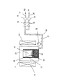
図1は実施例1に用いられた結晶成長装置の構成例を示す図である。 FIG. 1 is a diagram illustrating a configuration example of a crystal growth apparatus used in the first embodiment.
図1の結晶成長装置は、ステンレス製の閉じた形状の反応容器11に、アルカリ金属とIII族金属を含む融液25を保持し、結晶成長を行なうための融液保持容器12が設けられている。
The crystal growth apparatus of FIG. 1 is provided with a
この融液保持容器12は反応容器11から取り外すことができる。また、融液保持容器12の材質はBNである。
The
また、反応容器11の内部空間23に窒素原料となる窒素(N2)ガスを充満させ、かつ反応容器11内の窒素(N2)圧力を調整することを可能にするガス供給管14が反応容器11を貫通して装着されている。ここで、窒素ガスの圧力は圧力制御装置16で調整する事ができる。
Further, the
また、ガス供給管14はバルブ18で分岐し、Arガスを導入することができる。ここで、Arガスの圧力は圧力制御装置19で調整する事ができる。
The
また、反応容器11内の全圧力は圧力計22でモニターされる。
The total pressure in the
また、反応容器11の外側にはヒーター13が設置されている。
A
反応容器11はバルブ21の部分で結晶成長装置から取り外すことが可能であり、反応容器11の部分のみをグローブボックスに入れて作業することができる。
The
以下に、図1の結晶成長装置を使用した実施例1でのGaNの結晶成長方法を説明する。 The GaN crystal growth method in Example 1 using the crystal growth apparatus of FIG. 1 will be described below.
まず、反応容器11をバルブ21の部分で結晶成長装置から分離し、Ar雰囲気のグローブボックスに入れる。
First, the
次いで、BN製の融液保持容器12に、III族金属原料としてGaを入れ、アルカリ金属としてナトリウム(Na)を入れる。融液25中のNaの比率はNa/(Na+Ga)=0.7とした。また、Li原料としてLi3Nを入れた。
Next, Ga is added to the BN
次いで、融液保持容器12を融液保持容器保持台26に置き、反応容器11内に設置する。次いで、反応容器11を密閉し、バルブ21を閉じ、反応容器11内部を外部雰囲気と遮断する。次いで、反応容器11をグローブボックスから出し、結晶成長装置に組み込む。すなわち、反応容器11をヒーター13がある所定の位置に設置し、バルブ21の部分で窒素とアルゴンのガス供給ライン14に接続する。
Next, the
次いで、バルブ15,21を開け、反応容器11内に窒素ガスを入れる。このとき、圧力制御装置16で窒素圧力を3.3 MPaにした。この圧力は、本実施例で使用した装置において、結晶成長温度(775℃)に昇温したときに、反応容器11内の全圧が4MPaになる圧力である。
Next, the
次いで、バルブ15を閉じる。次いで、バルブ18を開け、反応容器11内にArガスを入れる。このとき、圧力制御装置19で圧力を6.6MPaにした。この場合、反応容器11内のArの分圧は3.3MPaとなる。この圧力(6.6MPa)は、本実施例で使用した装置において、結晶成長温度(775℃)に昇温したときに、反応容器11内の全圧が8MPaになる圧力である。すなわち窒素とArの分圧がそれぞれ4MPaとなる圧力である。
Next, the
次いで、バルブ18とバルブ21を閉じる。これにより、反応容器11は密閉される。次いで、ヒーター13に通電し、融液25を室温(27℃)から結晶成長温度まで1時間で昇温する。結晶成長温度は775℃とした。昇温に追随して密閉された反応容器11内の圧力は上昇し、結晶成長温度775℃に達した時の反応容器11内の全圧は8MPaになった。すなわち窒素とArの分圧はそれぞれ4MPaとなった。
Next, the
この状態で300時間保持した後、室温まで降温する。結晶成長終了後、反応容器11を開けると、融液保持容器12の内壁に無色透明な板状のGaN30が成長していた。
After maintaining for 300 hours in this state, the temperature is lowered to room temperature. When the
同様の結晶成長を融液中にLiを入れずに行なった場合には、小さな柱状結晶とc面を主面とする薄い板状のGaNが多数成長した。これに対し、融液中にLiを混合した場合には、図2に示すような大きな板状のGaN結晶30のみが成長した。
When the same crystal growth was performed without adding Li in the melt, a large number of small columnar crystals and thin plate-like GaN having a c-plane as the main surface grew. On the other hand, when Li was mixed in the melt, only a large plate-
成長した板状のGaN結晶30は、C面の差し渡しの長さが4mm以上で、厚さが80μm以上の大きさであった。X線ロッキングカーブの半値幅が45−55arcsecと狭く、欠陥密度はエッチピット密度評価で106cm−2以下であった。また、高抵抗で半絶縁性であった。
The grown plate-
実施例2は、第3,第4,第5,第6の形態に対応した実施例である。この実施例2では、アルカリ金属としてNa(ナトリウム)を使用し、III族元素の原料として金属Ga(ガリウム)を使用し、窒素原料として窒素ガスを使用し、さらに、Li(リチウム)の原料としてLi3N(窒化リチウム)を添加し、種結晶にIII族窒化物としてGaNを結晶成長させた。 Example 2 is an example corresponding to the third, fourth, fifth and sixth modes. In Example 2, Na (sodium) is used as an alkali metal, metal Ga (gallium) is used as a group III element source, nitrogen gas is used as a nitrogen source, and further, a Li (lithium) source is used. Li 3 N (lithium nitride) was added, and GaN was grown as a group III nitride on the seed crystal.
ここで、Na,Ga,Li3Nはあらかじめ混合融液として融液保持容器中に保持し、窒素は結晶成長中に気相から融液中に溶解して供給し、GaNを結晶成長させた。 Here, Na, Ga, Li 3 N was previously held in the melt holding container as a mixed melt, and nitrogen was dissolved and supplied from the gas phase into the melt during crystal growth, so that GaN was crystal grown. .
また、種結晶には、c面を主面とする板状のGaN結晶を使用した。 In addition, a plate-like GaN crystal having a c-plane as a main surface was used as a seed crystal.
図3は実施例2に用いた結晶成長装置の構成例を示す図である。図3の結晶成長装置は、図1の装置と同様のものである。 FIG. 3 is a diagram illustrating a configuration example of the crystal growth apparatus used in the second embodiment. The crystal growth apparatus of FIG. 3 is the same as the apparatus of FIG.
以下に、図3の結晶成長装置を使用した実施例2でのGaNの結晶成長方法を説明する。 Below, the crystal growth method of GaN in Example 2 using the crystal growth apparatus of FIG. 3 is demonstrated.
まず、反応容器11をバルブ21の部分で結晶成長装置から分離し、Ar雰囲気のグローブボックスに入れる。
First, the
次いで、BN製の融液保持容器12に、c面を主面とする板状GaN結晶32を種結晶として入れる。次いで、III族金属原料としてGaを入れ、アルカリ金属としてナトリウム(Na)を入れる。融液25中のNaの比率はNa/(Na+Ga)=0.4とした。次いで、Li原料としてLi3Nを入れた。
Next, a plate-
次いで、融液保持容器12を融液保持容器保持台26に置き、反応容器11内に設置する。その後は、実施例1と同様の手順で結晶成長を行った。
Next, the
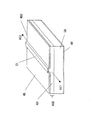
300時間の結晶成長後、種結晶32上には、図4に示すように表面が平坦で無色透明な板状のGaN結晶33が成長していた。
After crystal growth for 300 hours, a plate-
同様の結晶成長を融液中にLiを入れずに行なった場合には、種結晶32上には、図5に示すように表面の凹凸の大きいGaN結晶34が成長していた。これに対し、融液中にLiを混合した場合には、図4に示すような平坦な表面を有するGaN結晶33が成長した。
When the same crystal growth was performed without putting Li in the melt, a
成長したGaN33は、X線ロッキングカーブの半値幅が45−55arcsecと狭く、欠陥密度はエッチピット密度評価で106cm−2以下であった。また、高抵抗で半絶縁性であった。
The grown
実施例3は、第8の形態の半導体デバイス(発光素子)の一実施例である半導体レーザーである。 Example 3 is a semiconductor laser which is an example of the semiconductor device (light emitting element) of the eighth mode.
図6,図7は実施例3の半導体レーザーを示す図である。なお、図6は実施例3の半導体レーザーの斜視図であり、また、図7はその光出射方向に垂直な面での断面図である。 6 and 7 are diagrams showing a semiconductor laser of Example 3. FIG. FIG. 6 is a perspective view of the semiconductor laser of Example 3, and FIG. 7 is a cross-sectional view taken along a plane perpendicular to the light emitting direction.
実施例3の半導体レーザーは第6の形態のGaN結晶で作製したn型GaN基板50上に積層したIII族窒化物半導体積層構造で作製されている。
The semiconductor laser of Example 3 is manufactured with a group III nitride semiconductor multilayer structure laminated on an n-
すなわち、図6,図7において、半導体レーザー積層構造400は、250μmの厚さのn型GaN基板50上に、n型GaN層40、n型Al0.2Ga0.8Nクラッド層41、n型GaN光ガイド層42、In0.05Ga0.95N/In0.15Ga0.85N量子井戸活性層43、p型GaN光ガイド層44、p型Al0.2Ga0.8Nクラッド層45、p型GaNキャップ層46が順次積層された構造であり、MOCVD法で結晶成長されて作製されている。
That is, in FIGS. 6 and 7, a semiconductor laser stacked
そして積層構造400は、p型GaNキャップ層46からp型Al0.2Ga0.8Nクラッド層45の途中までをストライプ状に残してエッチングされ、電流狭窄リッジ導波路構造51が作製されている。この電流狭窄リッジ導波路構造はGaN基板の<1−100>方向に沿って形成されている。
Then, the
また、積層構造の表面には、SiO2からなる絶縁膜47が形成されている。リッジ51上の絶縁膜47には、開口部が形成されている。この開口部で露出したp型GaNキャップ層46表面に、p側のオーミック電極48が形成されている。
An insulating
また、n型GaN基板50の裏面には、n側のオーミック電極49が形成されている。n側オーミック電極49としては、Ti/Alを、p側オーミック電極48としては、Ni/Auを蒸着して形成した。
An n-
また、リッジ51と活性層43に垂直に光共振器面401,402が形成されている。光共振器面401,402はGaN基板の<1−100>方向に沿った電流狭窄リッジ導波路構造51に垂直な(1−100)面をへき開することにより形成されている。
Optical resonator surfaces 401 and 402 are formed perpendicular to the
n側オーミック電極49と光共振器面401,402は、n型GaN基板50の裏面を80μmまで研磨した後に形成した。
The n-
実施例3の半導体レーザーでは、p側のオーミック電極48とn側のオーミック電極49に電流を注入することによって、活性層にキャリアが注入され、発光、光の増幅が起り、光共振器面401,402から、レーザー光411,412が出射される。
In the semiconductor laser of Example 3, carriers are injected into the active layer by injecting current into the p-
実施例3の半導体レーザーは、従来のサファイア基板等のIII族窒化物と異なる基板上にレーザー構造を結晶成長して作製されたものや、気相成長や、その他の手法で作製されたGaN基板上に作製されたものに比べ、基板上に積層されたレーザー構造の結晶欠陥が低く、結晶品質が高いので、高出力動作下においても長寿命であった。 The semiconductor laser of Example 3 is produced by crystal growth of a laser structure on a substrate different from Group III nitride such as a conventional sapphire substrate, or a GaN substrate produced by vapor phase growth or other methods. Compared with the one produced above, the crystal structure of the laser structure laminated on the substrate is low and the crystal quality is high, so it has a long life even under high output operation.
実施例4は第9の形態の半導体デバイス(受光素子)の一実施例である。図8は実施例4の受光素子を示す図である。 Example 4 is an example of the semiconductor device (light receiving element) of the ninth mode. FIG. 8 is a diagram illustrating a light receiving element according to the fourth embodiment.
実施例4の受光素子は、第6の形態のIII族窒化物結晶で作製したn型GaN基板60上に積層したIII族窒化物半導体積層構造で作製されている。
The light receiving element of Example 4 is manufactured by a group III nitride semiconductor multilayer structure stacked on an n-
ここで、GaN基板60の厚さは、300μmである。
Here, the thickness of the
実施例4の受光素子の構造は、n型GaN基板60上に、n型GaN層61,絶縁性GaN層62が積層され、その上に、Ni/Auから成る透明ショットキー電極63が形成されたMIS型受光素子である。
In the structure of the light receiving element of Example 4, an n-
n型GaN基板60の裏面には、Ti/Alからなるオーミック電極64が形成され、透明ショットキー電極63の上部の一部には、Auからなる電極65が形成されている。
An
実施例4の受光素子では、透明ショットキー電極63側から光(紫外線)601を入射すると、キャリアが発生し、電極から光電流が取り出される。
In the light receiving element of Example 4, when light (ultraviolet light) 601 is incident from the
実施例4の受光素子は、従来のサファイア基板等のIII族窒化物と異なる基板上に受光素子構造を結晶成長して作製されたものや、気相成長や、その他の手法で作製されたGaN基板上に作製されたものに比べ、基板上に積層された受光素子構造の結晶欠陥が低く、結晶品質が高いので、暗電流が小さく、S/N比が高かった。 The light-receiving element of Example 4 is manufactured by crystal-growing the light-receiving element structure on a substrate different from the group III nitride such as a conventional sapphire substrate, GaN manufactured by vapor phase growth, or other methods. Compared to those fabricated on the substrate, the light-receiving element structure laminated on the substrate had low crystal defects and high crystal quality, so the dark current was small and the S / N ratio was high.
実施例5は第10の形態の半導体デバイス(電子デバイス)の一実施例である。図9は実施例5の半導体デバイス(電子デバイス)の断面図である。実施例5の電子デバイスは高電子移動度トランジスター(HEMT)である。 Example 5 is an example of the semiconductor device (electronic device) according to the tenth aspect. FIG. 9 is a cross-sectional view of a semiconductor device (electronic device) of Example 5. The electronic device of Example 5 is a high electron mobility transistor (HEMT).
実施例5の高電子移動度トランジスター(HEMT)は、Liを添加して結晶成長した第6の形態の高抵抗GaN結晶で作製したGaN基板70上に積層したIII族窒化物半導体積層構造で作製されている。
The high electron mobility transistor (HEMT) of Example 5 is manufactured with a group III nitride semiconductor stacked structure stacked on a
ここで、GaN基板70の厚さは、300μmである。
Here, the thickness of the
高電子移動度トランジスター(HEMT)の構造は、GaN基板70上に積層された絶縁性GaN層71、n型AlGaN層72、n型GaN層73からなるリセスゲートHEMTである。
The structure of the high electron mobility transistor (HEMT) is a recess gate HEMT including an insulating
n型GaN層73はゲート部分がn型AlGaN層72までエッチングされ、n型AlGaN層72にNi/Auからなるゲート電極76が形成されている。ゲートをはさんで両脇のn型GaN層73には、Ti/Alからなるドレイン電極75、ソース電極74がそれぞれ形成されている。
The gate portion of the n-
実施例5の高電子移動度トランジスター(HEMT)は、従来のサファイア基板等のIII族窒化物と異なる基板上に高電子移動度トランジスター(HEMT)構造を結晶成長して作製されたものや、気相成長や、その他の手法で作製されたGaN基板上に作製されたものに比べ、基板上に積層された高電子移動度トランジスター(HEMT)構造の結晶欠陥が低く、結晶品質が高いので、欠陥による電極の異常拡散や短絡が抑制され、耐圧が高く、また、良好な周波数特性を示した。 The high electron mobility transistor (HEMT) of Example 5 was prepared by crystal growth of a high electron mobility transistor (HEMT) structure on a substrate different from a group III nitride such as a conventional sapphire substrate, Compared to those grown on GaN substrates produced by phase growth or other methods, the crystal defects of the high electron mobility transistor (HEMT) structure stacked on the substrate are low and the crystal quality is high, so defects An abnormal diffusion and short circuit of the electrode due to, was suppressed, the withstand voltage was high, and good frequency characteristics were exhibited.
実施例6は第11の形態のシステムの一実施例である。すなわち、実施例6は第8の形態の半導体デバイス(発光素子)を具備した照明装置である。 Example 6 is an example of the system of the eleventh aspect. That is, Example 6 is an illuminating device including the semiconductor device (light emitting element) of the eighth mode.
図10は実施例6の照明装置の模式図である。また、図11は実施例6の照明装置の回路図である。また、図12は実施例6の照明装置の光源である白色LEDモジュールの断面図である。また、図13は白色LEDのモジュールの光源である紫外発光LEDの断面図である。 FIG. 10 is a schematic diagram of a lighting apparatus according to the sixth embodiment. FIG. 11 is a circuit diagram of the illumination device of the sixth embodiment. FIG. 12 is a cross-sectional view of a white LED module that is a light source of the illumination device of the sixth embodiment. FIG. 13 is a cross-sectional view of an ultraviolet light emitting LED which is a light source of a white LED module.
実施例6の照明装置は、2個の白色LEDモジュール902と電流制限抵抗96,直流電源97,スイッチ98とが直列に接続されており、スイッチ98のオン,オフによって、白色LEDモジュール902を発光させるようになっている。
In the illumination device of the sixth embodiment, two
ここで、白色LEDモジュール902は、紫外発光LED90にYAG系蛍光体91が塗布された構造をなす。そして、電極端子94,95間に所定の電圧を印加すると、紫外発光LED90が発光し、その紫外光によってYAG系蛍光体91が励起され、白色光901が取り出される。
Here, the
ここで、紫外発光LED90は、第6の形態のIII族窒化物結晶で作製したn型GaN基板80上に積層したIII族窒化物半導体積層構造で作製されている。
Here, the ultraviolet
GaN基板80の厚さは、300μmである。
The thickness of the
紫外発光LED90の構造は、n型GaN基板80上に、n型GaN層81、n型Al0.1Ga0.9N層82、InGaN/GaN多重量子井戸構造を有する活性層83、p型Al0.1Ga0.9N層84、p型GaN層85が積層され、その上に、Ni/Auから成る透明オーミック電極86が形成されている。透明オーミック電極86上には、Ni/Auから成るワイヤーボンディング用の電極87が形成されている。また、n型GaN基板80の裏面には、Ti/Alからなるオーミック電極88が形成されている。
The structure of the ultraviolet
この紫外発光LED90では、p側の電極87とn側のオーミック電極88に電流を注入することによって、活性層にキャリアが注入され、発光し、LED外部に紫外光801が取り出される。
In this ultraviolet
この実施例6のLEDは、従来のサファイア基板等のIII族窒化物と異なる基板上にLED構造を結晶成長して作製されたものや、気相成長や、その他の手法で作製されたGaN基板上に作製されたものに比べ、基板上に積層されたLED構造の結晶欠陥が低く、結晶品質が高いので、発光効率が高く、高出力動作する。 The LED of Example 6 is manufactured by crystal-growing an LED structure on a substrate different from a group III nitride such as a conventional sapphire substrate, or a GaN substrate manufactured by vapor phase growth or other methods. Compared with the one produced above, the crystal structure of the LED structure laminated on the substrate is low and the crystal quality is high, so the luminous efficiency is high and the output operation is high.
従って、実施例6の照明器具は、従来のサファイア基板等のIII族窒化物と異なる基板上にLED構造を結晶成長して作製されたものや、気相成長や、その他の手法で作製されたGaN基板上に作製された紫外LEDを使用した白色LED照明器具よりも、明るく、低消費電力である。 Therefore, the lighting fixture of Example 6 was produced by crystal-growing the LED structure on a substrate different from the group III nitride such as a conventional sapphire substrate, or by vapor phase growth or other methods. It is brighter and consumes less power than white LED lighting fixtures that use ultraviolet LEDs fabricated on a GaN substrate.
本発明は、光ディスク用青紫色光源、紫外光源(LD、LED)、電子写真用青紫色光源、III族窒化物電子デバイスなどに利用可能である。
The present invention can be used for a blue-violet light source for optical disks, an ultraviolet light source (LD, LED), a blue-violet light source for electrophotography, a group III nitride electronic device, and the like.
11 反応容器
12 融液保持容器
13 ヒーター
14 ガス供給管
15,18,21 バルブ
16,19 圧力調整器
17 窒素供給管
20 アルゴン供給管
22 圧力計
23 内部空間
24 原料GaN保持容器
25 融液
26 融液保持容器保持台
30 GaN柱状結晶
31 GaN柱状結晶
32 GaN種結晶
33 成長したGaN結晶
34 従来方法で成長したGaN結晶
40 n型GaN層
41 n型Al0.2Ga0.8Nクラッド層
42 n型GaN光ガイド層
43 In0.05Ga0.95N/In0.15Ga0.85N量子井戸活性層
44 p型GaN光ガイド層
45 p型Al0.2Ga0.8Nクラッド層
46 p型GaNキャップ層
47 絶縁膜
48 p側のオーミック電極
49 n側のオーミック電極
50 n型GaN基板
51 電流狭窄リッジ導波路構造
60 n型GaN基板
61 n型GaN層
62 絶縁性GaN層
63 透明ショットキー電極
64 オーミック電極
65 電極
70 GaN基板
71 絶縁性GaN層
72 n型AlGaN層
73 n型GaN層
74 ソース電極
75 ドレイン電極
76 ゲート電極
80 n型GaN基板
81 n型GaN層
82 n型Al0.1Ga0.9N層
83 InGaN/GaN多重量子井戸構造を有する活性層
84 p型Al0.1Ga0.9N層
85 p型GaN層
86 透明オーミック電極
87 電極
88 n側のオーミック電極
90 紫外発光LED
91 YAG系蛍光体
92 金ワイヤー
93 レンズ
94、95 電極端子
96 電流制限抵抗
97 直流電源
98 スイッチ
400 積層構造
401、402 光共振器面
411、412 レーザー光
601 光(紫外線)
801 紫外光
901 白色光
902 白色LEDモジュール
DESCRIPTION OF SYMBOLS 11 Reaction container 12 Melt holding container 13 Heater 14 Gas supply pipe 15, 18, 21 Valve 16, 19 Pressure regulator 17 Nitrogen supply pipe 20 Argon supply pipe 22 Pressure gauge 23 Internal space 24 Raw material GaN holding container 25 Melt 26 Melting Liquid holding vessel holding table 30 GaN columnar crystal 31 GaN columnar crystal 32 GaN seed crystal 33 GaN crystal grown 34 GaN crystal grown by conventional method 40 n-type GaN layer 41 n-type Al 0.2 Ga 0.8 N cladding layer 42 n-type GaN optical guide layer 43 In 0.05 Ga 0.95 N / In 0.15 Ga 0.85 N quantum well active layer 44 p-type GaN optical guide layer 45 p-type Al 0.2 Ga 0.8 N cladding Layer 46 p-type GaN cap layer 47 Insulating film 48 Ohmic electrode on p side 49 Ohmic electrode on n side 50 n-type Ga N substrate 51 Current confinement ridge waveguide structure 60 n-type GaN substrate 61 n-type GaN layer 62 insulating GaN layer 63 transparent Schottky electrode 64 ohmic electrode 65 electrode 70 GaN substrate 71 insulating GaN layer 72 n-type AlGaN layer 73 n-type GaN layer 74 Source electrode 75 Drain electrode 76 Gate electrode 80 n-type GaN substrate 81 n-type GaN layer 82 n-type Al 0.1 Ga 0.9 N layer 83 active layer having InGaN / GaN multiple quantum well structure 84 p-type Al 0.1 Ga 0.9 N layer 85 p-type GaN layer 86 transparent ohmic electrode 87 electrode 88 n-side ohmic electrode 90 ultraviolet light emitting LED
91
801
Claims (11)
Priority Applications (4)
| Application Number | Priority Date | Filing Date | Title |
|---|---|---|---|
| JP2004013562A JP2005206409A (en) | 2004-01-21 | 2004-01-21 | Method for growing group iii nitride crystal, group iii nitride crystal, semiconductor device, and system |
| US10/765,502 US7261775B2 (en) | 2003-01-29 | 2004-01-28 | Methods of growing a group III nitride crystal |
| US11/878,125 US7828896B2 (en) | 2003-01-29 | 2007-07-20 | Methods of growing a group III nitride crystal |
| US12/891,504 US20110012235A1 (en) | 2003-01-29 | 2010-09-27 | Method of growing group iii nitride crystal, group iii nitride crystal grown thereby, group iii nitride crystal growing apparatus and semiconductor device |
Applications Claiming Priority (1)
| Application Number | Priority Date | Filing Date | Title |
|---|---|---|---|
| JP2004013562A JP2005206409A (en) | 2004-01-21 | 2004-01-21 | Method for growing group iii nitride crystal, group iii nitride crystal, semiconductor device, and system |
Publications (1)
| Publication Number | Publication Date |
|---|---|
| JP2005206409A true JP2005206409A (en) | 2005-08-04 |
Family
ID=34899585
Family Applications (1)
| Application Number | Title | Priority Date | Filing Date |
|---|---|---|---|
| JP2004013562A Pending JP2005206409A (en) | 2003-01-29 | 2004-01-21 | Method for growing group iii nitride crystal, group iii nitride crystal, semiconductor device, and system |
Country Status (1)
| Country | Link |
|---|---|
| JP (1) | JP2005206409A (en) |
Cited By (3)
| Publication number | Priority date | Publication date | Assignee | Title |
|---|---|---|---|---|
| JP2007137735A (en) * | 2005-11-21 | 2007-06-07 | Ricoh Co Ltd | Group iii nitride crystal and its production method |
| JP2010056504A (en) * | 2008-07-31 | 2010-03-11 | Rohm Co Ltd | Semiconductor device |
| JP2011126777A (en) * | 2005-08-24 | 2011-06-30 | Mitsubishi Chemicals Corp | Method for producing group xiii metal nitride crystal and method of manufacturing semiconductor device |
-
2004
- 2004-01-21 JP JP2004013562A patent/JP2005206409A/en active Pending
Cited By (3)
| Publication number | Priority date | Publication date | Assignee | Title |
|---|---|---|---|---|
| JP2011126777A (en) * | 2005-08-24 | 2011-06-30 | Mitsubishi Chemicals Corp | Method for producing group xiii metal nitride crystal and method of manufacturing semiconductor device |
| JP2007137735A (en) * | 2005-11-21 | 2007-06-07 | Ricoh Co Ltd | Group iii nitride crystal and its production method |
| JP2010056504A (en) * | 2008-07-31 | 2010-03-11 | Rohm Co Ltd | Semiconductor device |
Similar Documents
| Publication | Publication Date | Title |
|---|---|---|
| US7828896B2 (en) | Methods of growing a group III nitride crystal | |
| JP4922268B2 (en) | Semiconductor laser | |
| US8231726B2 (en) | Semiconductor light emitting element, group III nitride semiconductor substrate and method for manufacturing such group III nitride semiconductor substrate | |
| JP2009046368A (en) | Sphalerite type nitride semiconductor self-supporting substrate, manufacturing method of sphalerite type nitride semiconductor self-supporting substrate and light-emitting device using sphalerite type nitride semiconductor self-supporting substrate | |
| JP4414241B2 (en) | Group III nitride crystal manufacturing method | |
| KR20070115969A (en) | Zinc oxide compound semiconductor light emitting element | |
| JP4560287B2 (en) | Group III nitride crystal manufacturing method | |
| JP2006287212A (en) | Nitride semiconductor light emitting device and method of fabricating the same | |
| JP4784922B2 (en) | Group III nitride crystal production method | |
| KR101067474B1 (en) | Semi-conductor light emitting device | |
| JP4508613B2 (en) | Group III nitride crystal manufacturing method | |
| Amano et al. | Defect and stress control of AlGaN for fabrication of high performance UV light emitters | |
| JP4551203B2 (en) | Group III nitride crystal manufacturing method | |
| JP2005206409A (en) | Method for growing group iii nitride crystal, group iii nitride crystal, semiconductor device, and system | |
| CN114497334A (en) | Semiconductor light-emitting element with hot carrier cooling layer | |
| JP5229103B2 (en) | Group III nitride crystal manufacturing method | |
| JP5310611B2 (en) | Group III nitride crystal manufacturing method | |
| JP2005206400A (en) | Method for growing group iii nitride crystal, group iii nitride crystal, semiconductor device, and system | |
| JP4414247B2 (en) | Group III nitride crystal manufacturing method | |
| JP4562398B2 (en) | Group III nitride crystal manufacturing method | |
| Amano et al. | Impact of low-temperature buffer layers on nitride-based optoelectronics | |
| Iwaya et al. | Fabrication of UV devices on various plane substrates | |
| JP4974742B2 (en) | Method for manufacturing light emitting device | |
| JPH11220166A (en) | Optical semiconductor device | |
| JP2000174336A (en) | GaN SEMICONDUCTOR LIGHT-EMITTING ELEMENT AND ITS MANUFACTURE |
Legal Events
| Date | Code | Title | Description |
|---|---|---|---|
| RD02 | Notification of acceptance of power of attorney |
Free format text: JAPANESE INTERMEDIATE CODE: A7422 Effective date: 20060201 |
|
| RD04 | Notification of resignation of power of attorney |
Free format text: JAPANESE INTERMEDIATE CODE: A7424 Effective date: 20060210 |
|
| A621 | Written request for application examination |
Free format text: JAPANESE INTERMEDIATE CODE: A621 Effective date: 20060517 |
|
| A977 | Report on retrieval |
Free format text: JAPANESE INTERMEDIATE CODE: A971007 Effective date: 20080910 |
|
| A131 | Notification of reasons for refusal |
Free format text: JAPANESE INTERMEDIATE CODE: A132 Effective date: 20080924 |
|
| A521 | Request for written amendment filed |
Free format text: JAPANESE INTERMEDIATE CODE: A523 Effective date: 20081125 |
|
| A131 | Notification of reasons for refusal |
Free format text: JAPANESE INTERMEDIATE CODE: A131 Effective date: 20090317 |
|
| A521 | Request for written amendment filed |
Free format text: JAPANESE INTERMEDIATE CODE: A523 Effective date: 20090514 |
|
| RD02 | Notification of acceptance of power of attorney |
Free format text: JAPANESE INTERMEDIATE CODE: A7422 Effective date: 20090730 |
|
| RD05 | Notification of revocation of power of attorney |
Free format text: JAPANESE INTERMEDIATE CODE: A7425 Effective date: 20090908 |
|
| A02 | Decision of refusal |
Free format text: JAPANESE INTERMEDIATE CODE: A02 Effective date: 20091124 |