JP2005202139A - Light emitting display device, and portable equipment having the light emitting display device, and method for driving the light emitting display device - Google Patents
Light emitting display device, and portable equipment having the light emitting display device, and method for driving the light emitting display device Download PDFInfo
- Publication number
- JP2005202139A JP2005202139A JP2004008109A JP2004008109A JP2005202139A JP 2005202139 A JP2005202139 A JP 2005202139A JP 2004008109 A JP2004008109 A JP 2004008109A JP 2004008109 A JP2004008109 A JP 2004008109A JP 2005202139 A JP2005202139 A JP 2005202139A
- Authority
- JP
- Japan
- Prior art keywords
- voltage
- display device
- emitting display
- boosting
- light emitting
- Prior art date
- Legal status (The legal status is an assumption and is not a legal conclusion. Google has not performed a legal analysis and makes no representation as to the accuracy of the status listed.)
- Granted
Links
Images

Abstract
Description
本発明は、複数のLED(Light Emitting Diode)を有する発光表示装置、及びこの発光表示装置を具備する携帯装置、及び発光表示装置の駆動方法に関するものである。 The present invention relates to a light emitting display device having a plurality of LEDs (Light Emitting Diodes), a portable device including the light emitting display device, and a driving method of the light emitting display device.
昨今、携帯電話のような携帯装置や各種の玩具・遊技機等には、複数のLEDからなる発光表示装置を内蔵したものが存在しており、しかも、使用するLEDには、赤色、緑色、青色、白色等の各色で発光するものが適宜用いられ、それぞれを所定のタイミングで発光させることにより、発光パターン等によって所定の状態であること等を表示可能としている。 Recently, portable devices such as mobile phones and various toys and gaming machines have built-in light-emitting display devices composed of a plurality of LEDs, and the LEDs to be used are red, green, Light emitting in each color such as blue and white is used as appropriate. By emitting each light at a predetermined timing, it is possible to display a predetermined state by a light emission pattern or the like.
このようなLEDでは、各色のLEDごとに、それぞれの発光に必要となる順方向電圧が異なっている。すなわち、赤色LEDの順方向電圧は約2.0Vであり、青色LED及び緑色LEDの順方向電圧は約3.0Vであり、白色LEDの順方向電圧は約3.5Vである。 In such an LED, the forward voltage required for each light emission is different for each color LED. That is, the forward voltage of the red LED is about 2.0V, the forward voltage of the blue LED and the green LED is about 3.0V, and the forward voltage of the white LED is about 3.5V.
したがって、省電力としながら各色のLEDをそれぞれ発光させるには、各LEDの順方向電圧に合わせた駆動電圧をLEDにそれぞれ印加することが望ましく、具体的には各LEDのカソードに電圧検出回路を接続し、この電圧検出回路でLEDに印加されている電圧を検出して、この検出値が所定の電圧値となるように制御することによって、省電力での発光表示装置の動作を可能としている(例えば、特許文献1参照。)。 Therefore, in order to make each color LED emit light while saving power, it is desirable to apply a driving voltage according to the forward voltage of each LED to each LED. Specifically, a voltage detection circuit is provided at the cathode of each LED. By connecting and detecting the voltage applied to the LED with this voltage detection circuit and controlling the detected value to be a predetermined voltage value, the operation of the light-emitting display device with power saving is enabled. (For example, refer to Patent Document 1).
このような発光表示装置を携帯装置に内蔵した場合には、発光表示装置を動作させる電源として、バッテリや乾電池等の使用にともなって出力電圧が低下する出力変動型の電源が用いられている。 When such a light-emitting display device is built in a portable device, an output-variable power source whose output voltage decreases with the use of a battery, a dry cell, or the like is used as a power source for operating the light-emitting display device.
この出力変動型の電源では、携帯装置の使用にともなって漸次出力電圧が低下して、携帯装置を動作させるために必要な必要電圧を出力できなくなるが、このように出力電圧が必要電圧を下回った場合でも、その後、電源はそれより小さい電圧での出力は可能であるので、この電圧を昇圧して必要電圧として出力する昇圧回路からなる昇圧装置を設けて、できるだけ携帯装置及び発光表示装置を長時間使用できるようにしている。
しかしながら、上記したように昇圧装置を設けた場合には、昇圧装置を動作させない非昇圧動作状態と、昇圧装置を動作させている昇圧動作状態とが切替わる出力電圧値の近傍において、非昇圧動作状態と昇圧動作状態を交互に繰返す昇圧装置の間欠動作が生じるという問題があった。 However, when the boosting device is provided as described above, the non-boosting operation is performed in the vicinity of the output voltage value at which the non-boosting operation state where the boosting device is not operated and the boosting operation state where the boosting device is operated are switched. There has been a problem that intermittent operation of the boosting device that alternately repeats the state and the boosting operation state occurs.
すなわち、出力変動型の電源から出力された出力電圧はほぼ一定の減衰率で低下するのではなく、発光表示装置や昇圧装置等の内部に設けた各回路の動作状態に応じて実際には電圧の上昇/下降の変動を繰り返しながら低下しているので、この変動が昇圧装置の動作/非動作の切替りの出力電圧値近傍で生じることによって、昇圧装置を間欠動作させることとなっていた。 In other words, the output voltage output from the output variation type power supply does not decrease with a substantially constant attenuation rate, but actually depends on the operating state of each circuit provided in the light emitting display device or booster device. Therefore, when the fluctuation occurs in the vicinity of the output voltage value for switching between operation / non-operation of the booster, the booster is operated intermittently.
特に、電源として電池を用いた場合には、電池の内部抵抗に起因して、この電池に接続した昇圧装置を含めた各種回路での消費電流値の変動にともなって電池電圧が大きく変動するために、昇圧装置の間欠動作を誘引させやすくなっていた。 In particular, when a battery is used as the power source, the battery voltage largely fluctuates due to fluctuations in current consumption in various circuits including the booster connected to the battery due to the internal resistance of the battery. In addition, it is easy to induce intermittent operation of the booster.
しかも、昇圧装置が動作した場合に、昇圧装置に入力される電源電圧と、昇圧装置から出力される昇圧電圧とが略同一電圧となっている場合には発振動作が生じることがあり、このような発振動作や先に述べた昇圧装置の間欠動作が生じた場合には、装置内部でのノイズ源となって発光表示装置や昇圧装置や周辺の装置の動作に悪影響を与えるおそれがあった。 In addition, when the booster operates, an oscillation operation may occur if the power supply voltage input to the booster and the boosted voltage output from the booster are substantially the same voltage. When the oscillation operation or the intermittent operation of the boosting device described above occurs, there is a possibility that the operation of the light emitting display device, the boosting device, and peripheral devices may be adversely affected as a noise source inside the device.
さらに、昇圧回路等の回路は、一般的に起動時に多大な回路電流の消費が生じるために、昇圧回路が動作/非動作を繰返すことによって多大な電流消費を繰返し、電源の電力消費の増大を招くおそれがあった。 In addition, since a circuit such as a booster circuit generally consumes a large amount of circuit current at the time of starting, the booster circuit repeats a large amount of current consumption by repeating operation / non-operation, thereby increasing the power consumption of the power supply. There was a risk of inviting.
そこで、本発明の発光表示装置では、LEDと、このLEDを駆動させる電源と、この電源から出力された電源電圧を昇圧する昇圧手段とを有する発光表示装置において、電源電圧の所定の電圧値である第1の電圧と、電源電圧と昇圧手段から出力された電圧との所定の電圧差である第2の電圧とを検出する電圧検出手段を設け、昇圧手段は、第1の電圧が検出されたときに動作を開始して、LEDを駆動させることができる必要最低限の電圧値となるように電源電圧を昇圧するとともに、動作開始後に、第2の電圧が検出されたときに動作を停止するように構成した。 Therefore, in the light emitting display device of the present invention, in a light emitting display device having an LED, a power source for driving the LED, and a boosting means for boosting the power supply voltage output from the power source, the light emitting display device has a predetermined power supply voltage value. Voltage detecting means for detecting a first voltage and a second voltage that is a predetermined voltage difference between the power supply voltage and the voltage output from the boosting means is provided, and the boosting means detects the first voltage. When the operation starts, the power supply voltage is boosted so that the required minimum voltage value can drive the LED. After the operation starts, the operation stops when the second voltage is detected. Configured to do.
さらに、電圧検出手段は、LEDのカソードと接続した第1電圧検出手段と、電源と昇圧手段とに接続した第2電圧検出手段とで構成し、第1電圧検出手段で第1の電圧を検出するとともに、第2電圧検出手段で第2の電圧を検出することにも特徴を有し、昇圧手段の動作と非動作の切替えを、第1の電圧の検出に基づいて第1電圧検出手段が出力する第1の検出信号と、第2の電圧の検出に基づいて第2電圧検出手段が出力する第2の検出信号とを切替制御手段に入力して行うとともに、この切替制御手段には、第1の検出信号と第2の検出信号とをそれぞれ所定時間だけ遅延させた第1の遅延検出信号と第2の遅延検出信号とをそれぞれ入力するように構成したことにも特徴を有するものである。 Further, the voltage detection means includes a first voltage detection means connected to the cathode of the LED and a second voltage detection means connected to the power source and the boosting means, and the first voltage detection means detects the first voltage. In addition, the second voltage detection means has a feature that the second voltage detection means detects the second voltage, and the first voltage detection means switches between the operation and non-operation of the boosting means based on the detection of the first voltage. The first detection signal to be output and the second detection signal output from the second voltage detection means based on detection of the second voltage are input to the switching control means, and the switching control means includes The first detection signal and the second detection signal obtained by delaying the first detection signal and the second detection signal by a predetermined time are input, respectively. is there.
また、本発明の発光表示装置の駆動方法では、LEDと、このLEDを駆動させる電源と、この電源から出力された電源電圧を昇圧する昇圧手段とを有する発光表示装置の駆動方法において、電源電圧の所定の電圧値である第1の電圧と、電源電圧と昇圧手段から出力された電圧との所定の電圧差である第2の電圧とを検出する電圧検出手段を設け、電圧検出手段で第1の電圧を検出したときには、昇圧手段を動作させてLEDを駆動させることができる必要最低限の電圧値となるように電源電圧を昇圧するとともに、昇圧手段の動作開始後に、電圧検出手段が第2の電圧を検出したときには、昇圧手段の動作を停止させることとした。 Further, in the driving method of the light emitting display device of the present invention, in the driving method of the light emitting display device having the LED, the power source for driving the LED, and the boosting means for boosting the power source voltage output from the power source. Voltage detecting means for detecting a first voltage that is a predetermined voltage value of the first voltage and a second voltage that is a predetermined voltage difference between the power supply voltage and the voltage output from the boosting means. When the voltage of 1 is detected, the power supply voltage is boosted so that the boosting means operates and the LED can be driven, and the voltage detecting means When the voltage of 2 is detected, the operation of the boosting means is stopped.
また、本発明の携帯装置では、複数のLEDと、これらのLEDを駆動させる電池と、この電池から出力された電源電圧を昇圧する昇圧手段とから構成した発光表示装置を具備する携帯装置において、電源電圧の所定の電圧値である第1の電圧と、電源電圧と昇圧手段から出力された電圧との所定の電圧差である第2の電圧とを検出する電圧検出手段を設け、昇圧手段は、第1の電圧が検出されたときに動作を開始して、発光しているLEDのうち最大の順方向電圧値を有するLEDを駆動させることができる必要最低限の電圧値となるように電源電圧を昇圧するとともに、動作開始後に、第2の電圧が検出されたときに動作を停止するように構成した。 Further, in the portable device of the present invention, in the portable device comprising a light emitting display device composed of a plurality of LEDs, a battery for driving these LEDs, and a boosting means for boosting the power supply voltage output from the battery, Voltage detecting means for detecting a first voltage, which is a predetermined voltage value of the power supply voltage, and a second voltage, which is a predetermined voltage difference between the power supply voltage and the voltage output from the boosting means, is provided. The power supply starts to operate when the first voltage is detected so that the LED having the maximum forward voltage value among the LEDs emitting light can be driven to have the minimum voltage value necessary. The voltage is boosted, and the operation is stopped when the second voltage is detected after the operation is started.
請求項1記載の発明によれば、LEDと、このLEDを駆動させる電源と、この電源から出力された電源電圧を昇圧する昇圧手段とを有する発光表示装置において、電源電圧の所定の電圧値である第1の電圧と、電源電圧と昇圧手段から出力された電圧との所定の電圧差である第2の電圧とを検出する電圧検出手段を設け、昇圧手段は、第1の電圧が検出されたときに動作を開始して、LEDを駆動させることができる必要最低限の電圧値となるように電源電圧を昇圧するとともに、動作開始後に、第2の電圧が検出されたときに動作を停止するように構成したことによって、昇圧手段が非動作状態から動作状態に切替わる電源電圧の値と、昇圧手段が動作状態から非動作状態に切替わる電源電圧の値とを異ならせることができるので、電源電圧に上昇/下降の変動が生じても、昇圧手段が頻繁な間欠動作を行うことを抑制することができる。したがって、発光表示装置におけるノイズの低減や、省電力化を図ることができる。 According to the first aspect of the present invention, in a light emitting display device having an LED, a power source for driving the LED, and a boosting unit for boosting a power source voltage output from the power source, the light emitting display device has a predetermined voltage value of the power source voltage. Voltage detecting means for detecting a first voltage and a second voltage that is a predetermined voltage difference between the power supply voltage and the voltage output from the boosting means is provided, and the boosting means detects the first voltage. When the operation starts, the power supply voltage is boosted so that the required minimum voltage value can drive the LED. After the operation starts, the operation stops when the second voltage is detected. With this configuration, the value of the power supply voltage at which the boosting means is switched from the non-operating state to the operating state can be made different from the value of the power supply voltage at which the boosting means is switched from the operating state to the non-operating state. ,Power supply Even if fluctuations in the up / down in pressure is generated, boosting means can be prevented to perform frequent intermittent operation. Therefore, noise reduction and power saving in the light-emitting display device can be achieved.
請求項2記載の発明では、電圧検出手段は、LEDのカソードと接続した第1電圧検出手段と、電源と昇圧手段とに接続した第2電圧検出手段とで構成し、第1電圧検出手段で第1の電圧を検出するとともに、第2電圧検出手段で第2の電圧を検出することによって、第1電圧検出手段ではLEDにおける電圧の印加状態を検出する検出手段と兼用することができるので、電圧検出手段を簡潔に構成できる。また、第2電圧検出手段では他の回路等の影響を受けることなく第2の電圧を検出することができるので、昇圧手段の動作から非動作への切替えを精度よく行うことができる。 According to a second aspect of the present invention, the voltage detecting means comprises a first voltage detecting means connected to the cathode of the LED and a second voltage detecting means connected to the power source and the boosting means. By detecting the first voltage and detecting the second voltage with the second voltage detection means, the first voltage detection means can also be used as the detection means for detecting the application state of the voltage in the LED. The voltage detection means can be configured simply. In addition, since the second voltage detection means can detect the second voltage without being affected by other circuits or the like, it is possible to accurately switch the operation of the boosting means from non-operation.
請求項3記載の発明では、昇圧手段の動作と非動作の切替えを、第1の電圧の検出に基づいて第1電圧検出手段が出力する第1の検出信号と、第2の電圧の検出に基づいて第2電圧検出手段が出力する第2の検出信号とを切替制御手段に入力して行うとともに、この切替制御手段には、第1の検出信号と第2の検出信号とをそれぞれ所定時間だけ遅延させた第1の遅延検出信号と第2の遅延検出信号とをそれぞれ入力するように構成したことによって、第1の電圧の近傍、及び第2の電圧の近傍において電源電圧に上昇/下降の瞬間的な変動が生じてもその影響を受けにくくすることができ、発光表示装置をより安定的に動作させることができる。 According to the third aspect of the present invention, the switching between the operation and the non-operation of the boosting means is performed by detecting the first detection signal output from the first voltage detection means based on the detection of the first voltage and the detection of the second voltage. And the second detection signal output from the second voltage detection means is input to the switching control means, and the switching control means receives the first detection signal and the second detection signal for a predetermined time. The first delay detection signal and the second delay detection signal that are delayed by an amount of time are input to increase or decrease the power supply voltage in the vicinity of the first voltage and in the vicinity of the second voltage. Even if a momentary fluctuation occurs, it can be made less susceptible to the influence, and the light-emitting display device can be operated more stably.
請求項4記載の発明では、LEDと、このLEDを駆動させる電源と、この電源から出力された電源電圧を昇圧する昇圧手段とを有する発光表示装置の駆動方法において、電源電圧の所定の電圧値である第1の電圧と、電源電圧と昇圧手段から出力された電圧との所定の電圧差である第2の電圧とを検出する電圧検出手段を設け、電圧検出手段で第1の電圧を検出したときには、昇圧手段を動作させてLEDを駆動させることができる必要最低限の電圧値となるように電源電圧を昇圧するとともに、昇圧手段の動作開始後に、電圧検出手段が第2の電圧を検出したときには、昇圧手段の動作を停止させるようにしたことによって、請求項1記載の発明と同様に、昇圧手段が非動作状態から動作状態に切替わる電源電圧の値と、昇圧手段が動作状態から非動作状態に切替わる電源電圧の値とを異ならせることができるので、電源電圧に上昇/下降の変動が生じても、昇圧手段が頻繁な間欠動作を行うことを抑制することができる。したがって、発光表示装置におけるノイズの低減や、省電力化を図ることができる。 According to a fourth aspect of the present invention, in a driving method of a light-emitting display device having an LED, a power source for driving the LED, and a boosting means for boosting a power source voltage output from the power source, a predetermined voltage value of the power source voltage is provided. Voltage detecting means for detecting the first voltage and the second voltage, which is a predetermined voltage difference between the power supply voltage and the voltage output from the boosting means, is provided, and the first voltage is detected by the voltage detecting means. In this case, the power supply voltage is boosted so that the boosting means operates to drive the LED, and the voltage detecting means detects the second voltage after the boosting means starts operating. In this case, by stopping the operation of the boosting means, the power supply voltage value at which the boosting means is switched from the non-operating state to the operating state and the boosting means are operated as in the first aspect of the invention. Since the value of the power supply voltage that is switched from the state to the non-operation state can be made different, it is possible to prevent the boosting means from performing frequent intermittent operation even if the power supply voltage fluctuates up or down. . Therefore, noise reduction and power saving in the light-emitting display device can be achieved.
請求項5記載の発明では、複数のLEDと、これらのLEDを駆動させる電池と、この電池から出力された電源電圧を昇圧する昇圧手段とから構成した発光表示装置を具備する携帯装置において、電源電圧の所定の電圧値である第1の電圧と、電源電圧と昇圧手段から出力された電圧との所定の電圧差である第2の電圧とを検出する電圧検出手段を設け、昇圧手段は、第1の電圧が検出されたときに動作を開始して、発光しているLEDのうち最大の順方向電圧値を有するLEDを駆動させることができる必要最低限の電圧値となるように電源電圧を昇圧するとともに、動作開始後に、第2の電圧が検出されたときに動作を停止するように構成したことによって、請求項1記載の発明と同様に、昇圧手段が非動作状態から動作状態に切替わる電源電圧の値と、昇圧手段が動作状態から非動作状態に切替わる電源電圧の値とを異ならせることができるので、電源電圧に上昇/下降の変動が生じても、昇圧手段が頻繁な間欠動作を行うことを抑制して携帯装置の動作の安定化を図ることができる。 According to a fifth aspect of the present invention, in a portable device comprising a light emitting display device comprising a plurality of LEDs, a battery for driving these LEDs, and a boosting means for boosting the power supply voltage output from the battery, Voltage detection means for detecting a first voltage, which is a predetermined voltage value of the voltage, and a second voltage, which is a predetermined voltage difference between the power supply voltage and the voltage output from the boosting means, is provided. The operation starts when the first voltage is detected, and the power supply voltage is set to a minimum necessary voltage value capable of driving the LED having the maximum forward voltage value among the light-emitting LEDs. And the operation is stopped when the second voltage is detected after the operation is started, so that the boosting means is changed from the non-operating state to the operating state. Switch Since the value of the source voltage and the value of the power supply voltage at which the booster is switched from the operating state to the non-operating state can be made different, the booster is frequently intermittent even if the power supply voltage fluctuates up or down. The operation of the portable device can be stabilized by suppressing the operation.
本発明の発光表示装置、及びこの発光表示装置を具備する携帯装置、及び発光表示装置の駆動方法では、発光表示装置を、少なくともLEDと、このLEDを駆動させる電圧を出力する電源と、この電源から出力された電源電圧を昇圧する昇圧手段とで構成しており、さらに、電源電圧の所定の電圧値である第1の電圧と、電源電圧と昇圧手段から出力された電圧との所定の電圧差である第2の電圧とを検出する電圧検出手段を設けて、第1の電圧と第2の電圧とを用いて昇圧手段の動作/非動作の切替えを行っているものである。 In the light emitting display device of the present invention, the portable device including the light emitting display device, and the driving method of the light emitting display device, the light emitting display device includes at least an LED, a power source that outputs a voltage for driving the LED, and the power source. And a booster that boosts the power supply voltage output from the power supply voltage, and a first voltage that is a predetermined voltage value of the power supply voltage, and a predetermined voltage of the power supply voltage and the voltage output from the booster Voltage detecting means for detecting the second voltage which is the difference is provided, and the operation / non-operation of the boosting means is switched using the first voltage and the second voltage.
すなわち、昇圧手段では、電圧検出手段において第1の電圧が検出されたときに動作を開始して、LEDを駆動させることができる必要最低限の電圧値となるように電源電圧を昇圧するとともに、動作開始後に、電圧検出手段において第2の電圧が検出されたときに動作を停止するように構成しているものである。 That is, the boosting unit starts operation when the first voltage is detected by the voltage detecting unit, boosts the power supply voltage so as to obtain a minimum necessary voltage value capable of driving the LED, After the operation is started, the operation is stopped when the second voltage is detected by the voltage detection means.
このように、昇圧手段の動作/非動作の切替制御を第1の電圧と第2の電圧とを用いて行うことにより、電圧検出手段で検出している電源電圧に上昇/下降の変動が生じても、所定の電圧差に相当する電圧変動が生じないかぎりは昇圧手段の動作/非動作の切替えを行わせないようにすることができるので、昇圧手段が頻繁に間欠動作することを抑制できる。 As described above, when the operation control / non-operation switching control of the voltage boosting unit is performed using the first voltage and the second voltage, the power supply voltage detected by the voltage detection unit fluctuates. However, as long as there is no voltage fluctuation corresponding to a predetermined voltage difference, it is possible not to switch the operation / non-operation of the boosting means, so that it is possible to suppress frequent operation of the boosting means. .
したがって、昇圧手段の頻繁な間欠動作の抑制にともなってノイズの発生や電力消費を低減させることができ、発光表示装置を省電力で安定動作させることができる。 Therefore, generation of noise and power consumption can be reduced with the suppression of frequent intermittent operation of the boosting means, and the light emitting display device can be stably operated with power saving.
しかも、昇圧手段を動作させた場合には、発光しているLEDのうち最大の順方向電圧値を有するLEDを駆動させることができる必要最低限の電圧値となるように所定の大きさだけ電源電圧を昇圧することによって、電源電圧と昇圧手段によって昇圧されて出力された昇圧電圧とを略一致させないようにすることができ、発振動作の発生を抑制できる。 In addition, when the boosting means is operated, the power supply of a predetermined magnitude is used so that the necessary minimum voltage value capable of driving the LED having the maximum forward voltage value among the light emitting LEDs is driven. By boosting the voltage, it is possible to prevent the power supply voltage and the boosted voltage boosted by the boosting means from being substantially coincident with each other, thereby suppressing the occurrence of an oscillation operation.
上記した電圧検出手段は、LEDのカソードと接続した第1電圧検出手段と、電源と昇圧手段とに接続した第2電圧検出手段とで構成しており、第1電圧検出手段で第1の電圧を検出するとともに、第2電圧検出手段で第2の電圧を検出している。 The voltage detection means described above includes a first voltage detection means connected to the cathode of the LED and a second voltage detection means connected to the power source and the boosting means. The first voltage detection means uses the first voltage detection means. , And the second voltage detecting means detects the second voltage.
第2電圧検出手段は電源と昇圧手段とに接続することによって、第2電圧検出手段による第2の電圧の検出において発光表示装置内に設けた他の回路等の影響を受けることなく第2の電圧を検出することがで、昇圧手段の動作から非動作への切替制御の精度を向上させることができる。 The second voltage detection means is connected to the power source and the boosting means, so that the second voltage detection means can detect the second voltage without being influenced by other circuits provided in the light emitting display device. By detecting the voltage, it is possible to improve the accuracy of switching control from the operation of the boosting means to the non-operation.
一方、第1電圧検出手段はLEDのカソードと接続することによって、LEDに印加する電圧のフィードバック制御のために検出するLEDへの印加電圧を第1電圧検出手段で同時に行うことができ、発光表示装置の小型化を図ることができる。 On the other hand, by connecting the first voltage detecting means to the cathode of the LED, the applied voltage to the LED detected for feedback control of the voltage applied to the LED can be simultaneously performed by the first voltage detecting means. The size of the apparatus can be reduced.
昇圧手段の動作と非動作の切替えは、第1の電圧の検出に基づいて第1電圧検出手段が出力する第1の検出信号と、第2の電圧の検出に基づいて第2電圧検出手段が出力する第2の検出信号とを切替制御手段に入力して行っている。 The operation of the boosting means is switched between non-operation by the first detection signal output from the first voltage detection means based on the detection of the first voltage and the second voltage detection means based on the detection of the second voltage. The second detection signal to be output is input to the switching control means.
特に、この切替制御手段には、第1の検出信号と第2の検出信号とをそれぞれ信号遅延手段に入力して、この信号遅延手段において第1の検出信号と第2の検出信号とをそれぞれ所定時間だけ遅延させた第1の遅延検出信号と第2の遅延検出信号とを生成し、この第1の遅延検出信号と第2の遅延検出信号をそれぞれ入力するように構成している。 In particular, the switching control means inputs the first detection signal and the second detection signal to the signal delay means, respectively, and the signal delay means receives the first detection signal and the second detection signal, respectively. A first delay detection signal and a second delay detection signal delayed by a predetermined time are generated, and the first delay detection signal and the second delay detection signal are respectively input.
したがって、第1の電圧の近傍や第2の電圧の近傍において電源電圧に上昇/下降の瞬間的な変動が生じても、その影響を受けにくくすることができ、発光表示装置をより安定的に動作させることができる。 Therefore, even if a momentary increase / decrease in the power supply voltage occurs in the vicinity of the first voltage or the second voltage, it is possible to make the light-emitting display device more stable. It can be operated.
以下において、図面に基づいて本実施形態の携帯装置を詳説する。本実施形態の携帯装置は、発光表示装置を具備した携帯電話であって、電源には充電可能なバッテリを用いている。なお、携帯装置は携帯電話に限定するものではなく、携帯可能な電子機器であって発光表示装置を具備したもの、例えばデジタルスチルカメラ、携帯用ゲーム機、ペンライト、携帯用音楽プレーヤ、PDA(Personal Digital Assistant)、モバイル型のパーソナルコンピュータ等、いずれであってもよい。また、電源は充電が可能なバッテリからなる電池だけでなく、使い切りの乾電池であってもよく、電力供給が可能となっていればよい。以下において特に言及しない場合には、「電池」はバッテリ等の蓄電池や乾電池等の使用にともなって出力電圧が低下する出力変動型の電源を指すものとする。 Hereinafter, the portable device of the present embodiment will be described in detail based on the drawings. The mobile device of this embodiment is a mobile phone equipped with a light emitting display device, and uses a rechargeable battery as a power source. Note that the portable device is not limited to a cellular phone, and is a portable electronic device including a light emitting display device, such as a digital still camera, a portable game machine, a penlight, a portable music player, a PDA ( Personal Digital Assistant) or a mobile personal computer may be used. The power source is not limited to a rechargeable battery, but may be a dry battery that is used up as long as power can be supplied. Unless otherwise specified, “battery” refers to a power source of an output variation type in which the output voltage decreases with the use of a storage battery such as a battery or a dry battery.
図1に示すように、本発明の携帯装置Aに内蔵した発光表示装置10は、バッテリからなる電池11と、この電池11から供給された電圧、すなわち電源電圧を調整する電圧調整部12と、この電圧調整部12にアノードをそれぞれ接続したLED13a,13b,・・・,13nと、各LED13a,13b,・・・,13nのカソードと接続して各LED13a,13b,・・・,13nの駆動制御を行うLED発光電流駆動回路14a,14b,・・・,14nと、これらのLED発光電流駆動回路14a,14b,・・・,14nを制御する発光制御回路15とから構成している。
As shown in FIG. 1, the light emitting
さらに、発光表示装置10には、各LED13a,13b,・・・,13nのカソードと接続してそれぞれのLED13a,13b,・・・,13nに印加された電圧値を検出するとともに、その中での最低の電圧値を検出する最低電圧検出回路16を設け、この最低電圧検出回路16で検出された最低電圧値に基づいて、後述するように電圧調整部12によって各LED13a,13b,・・・,13nに印加する電圧を調整している。
Further, the light emitting
さらに、発光表示装置10には、最低電圧検出回路16と接続して第1電圧を検出する第1電圧検出手段である第1電圧検出回路17と、電池11と後述する昇圧回路12bとに接続して第2電圧を検出する第2電圧検出手段である第2電圧検出回路18と、この第1電圧検出回路17と第2電圧検出回路18からそれぞれ出力された第1検出信号及び第2検出信号を入力する信号遅延回路19と、この信号遅延回路19に接続した切替制御回路21を設けている。
Further, the light emitting
図1中、22は電池11から出力された電圧を昇圧するためのコイルであり、23は電圧調整部12から出力される電圧安定化のためのコンデンサである。
In FIG. 1, 22 is a coil for boosting the voltage output from the
説明の便宜上、電池11は発光表示装置10に含めているが、電池11は携帯装置Aの発光表示装置10以外の装置の電源として共用している。説明の便宜上、電池11から出力された電源電圧を、「電池出力電圧」と呼ぶことにする。
For convenience of explanation, the
電圧調整部12は、入力された電圧をそのまま出力するスルー回路12aと、入力された電圧を昇圧して出力する昇圧手段である昇圧回路12bと、昇圧回路12bにおける昇圧の電圧値を調整するためのヒステリシス調整回路12cと、入力された電圧をスルー回路12aと昇圧回路12bのいずれか一方に入力するために切替える切替回路12dとから構成している。なお、電圧調整部12の全体で一つの昇圧回路を構成していると見なしてもよい。
The
昇圧回路12bでは、後述するように最低電圧検出回路16から入力された最低電圧値に基づいて昇圧量を調整して、各LED13a,13b,・・・,13nに印加する電圧を調整している。
The
ヒステリシス調整回路12cは、図示しない調整用信号の入力によって、後述するように昇圧回路12bから出力する昇圧後の電圧である昇圧電圧を任意に調整可能としている。ヒステリシス調整回路12cに基づいて昇圧回路12bにおいて昇圧されて出力された電圧を「昇圧電圧」と呼ぶことにする。
The
切替回路12dは、切替制御回路21から入力された切替制御信号に基づいて、電池11から入力された電圧をスルー回路12aと昇圧回路12bのいずれか一方に入力することにより、モードの切り替えを行っている。すなわち、切替回路12dにおいてスルー回路12aを選択している場合には、スルーモードとして電池出力電圧を出力させ、切替回路12dにおいて昇圧回路12bを選択している場合には、昇圧モードとして昇圧電圧を出力させるようにしている。
Based on the switching control signal input from the switching
LED13a,13b,・・・,13nは、それぞれ所要の目的に応じて設けているものであり、互いに並列接続している。本実施形態の場合において、LED13a,13b,・・・,13nは、具体的には携帯電話からなる携帯装置Aの液晶表示装置のバックライト用LEDや、着信表示用のLED等であり、使用者の興味をそそるように異なる色で発光するLEDを複数設けている。なお、LEDは必ずしも複数設ける必要はなく、1個だけであってもよい。その場合には、最低電圧検出回路16は不要である。
The
各LED13a,13b,・・・,13nは、それぞれのカソードに接続したLED発光電流駆動回路14a,14b,・・・,14nによって駆動するようにしており、LED発光電流駆動回路14a,14b,・・・,14nは発光制御回路15から入力された駆動制御信号に基づいてそれぞれ駆動するようにしている。
Each
発光制御回路15には、発光表示装置10の外部に設けている携帯装置Aの制御回路(図示せず)からの発光出力信号が入力され、この発光出力信号に基づいて発光制御回路15において駆動制御信号を生成している。
A light emission output signal from a control circuit (not shown) of the portable device A provided outside the light emitting
各LED13a,13b,・・・,13nのカソードに接続した最低電圧検出回路16では、各LED13a,13b,・・・,13nに印加された電圧の値を検出するとともに、検出した電圧の値のうちで最低の電圧の値を検出している。最低電圧検出回路16で検出される電圧の値は、電圧調整部12から出力された電圧と、各LED13a,13b,・・・,13nの順方向電圧との差に相当する値であって、この電圧の値が正の値でない場合には、そのLEDには順方向電圧に相当するだけの電圧が供給されていないこととなっている。
The lowest
そこで、最低電圧検出回路16には所定のしきい値を設け、検出した電圧の値のうちで最低の電圧の値がしきい値より小さい場合には、その電圧の値を昇圧回路12bに入力して、後述するように電圧調整部12から昇圧電圧を出力させるように構成している。
Therefore, the minimum
第1電圧検出回路17には、最低電圧検出回路16から出力された最低の電圧の値を入力し、スルーモード時には、この電圧の値から電池出力電圧を算出して、電池出力電圧があらかじめ設定した第1電圧となった場合に第1検出信号を出力するように構成している。
The first
第1電圧は、各LED13a,13b,・・・,13nのうちで最大の順方向電圧を有するLEDの順方向電圧に、発光表示装置10を構成している各回路を動作させるために必要な電圧を足し合わせた電圧としている。
The first voltage is necessary for operating each circuit constituting the light emitting
最低電圧検出回路16を介して第1電圧検出回路17に各LED13a,13b,・・・,13nを接続した場合には、上記したように最低電圧検出回路16から出力された電圧の値に基づいて第1電圧の検出を行うとともに、昇圧回路12bにおける昇圧の適正な制御を可能とすることができる。
When the
なお、本実施形態では、第1電圧検出回路17は、最低電圧検出回路16を介して各LED13a,13b,・・・,13nのカソードに接続しているが、第1電圧を検出する目的のためには必ずしも最低電圧検出回路16を設ける必要はなく、第1電圧検出回路17を各LED13a,13b,・・・,13nのカソードに接続して第1電圧を検出するように構成してもよい。この場合には、複数設けたLED13a,13b,・・・,13nのいずれか一つのカソードに接続すればよく、全てのLED13a,13b,・・・,13nのカソードと第1電圧検出回路17とを接続する必要はない。
In the present embodiment, the first
また、本実施形態では、最低電圧検出回路16あるいは第1電圧検出回路17で各LED13a,13b,・・・,13nに印加された電圧を検出するようにしているが、各LED13a,13b,・・・,13nに印加された電圧の値が検出可能であれば、最低電圧検出回路16や第1電圧検出回路17以外の構成としてもよい。
In the present embodiment, the minimum
第2電圧検出回路18には、電池11から出力された電池出力電圧を入力するととともに、昇圧回路12bから出力された昇圧電圧を入力して、昇圧電圧と電池出力電圧との差電圧があらかじめ設定した第2電圧以下となった場合に第2検出信号を出力するように構成している。すなわち、第2電圧は、昇圧電圧と電池出力電圧との差電圧である(図2参照)。第2電圧検出回路18は電池11と接続したことによって、スルーモード及び昇圧モードに関わらず電池出力電圧から正確に第2電圧を検出することができ、しかも、他の回路の影響を受けることなく第2電圧を検出することができる。
The battery voltage output from the
他の実施形態として、第2電圧検出回路18には、電池11から出力された電圧を入力して電池出力電圧を検出し、電池出力電圧があらかじめ設定した電圧となった場合に第2検出信号を出力するように構成しもよい。
As another embodiment, the voltage output from the
信号遅延回路19では、第1電圧検出回路17から入力された第1検出信号、及び第2電圧検出回路18から入力された第2検出信号に基づいて、それぞれを所定時間だけ遅延させることにより第1遅延検出信号及び第2遅延検出信号を生成し、この第1遅延検出信号及び第2遅延検出信号を出力している。
The
切替制御回路21は、信号遅延回路19から入力された第1遅延検出信号及び第2遅延検出信号に基づいて、電圧調整部12の切替回路12dを切替えるための切替信号を出力している。この切替信号に基づいて、電圧調整部12では電池出力電圧と昇圧電圧のいずれか一方を出力している。
The switching
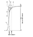
以下において、図2に示した電池11における電力の消費状態に対するLED駆動用入力電圧の相関図に基づいて、昇圧回路12bの動作について説明する。
Hereinafter, the operation of the
まず、電池11は、図2に示すように電力消費にともなって電池出力電圧が所定の特性曲線Pにしたがって低下する。ここで、説明の便宜上、電池出力電圧は、スルーモードにおいてはスルー回路12aで省電力化のための余計な出力調整を行うことなく適正な電力となっているものとする。
First, as shown in FIG. 2, the battery output voltage of the
発光表示装置10では、スルーモードにおいてはスルー回路12aから出力された電池出力電圧に基づいて所要のLED13a,13b,・・・,13nを発光させており、電池11の電力が消費される。
In the light emitting
電池11の電力が消費されることにより、電池出力電圧が第1電圧に近づいた場合には、特性曲線P上の第1パスR1に沿って第1電圧に達する。
When the battery output voltage approaches the first voltage due to the consumption of the
電池出力電圧が第1電圧に達すると、第1電圧検出回路17が第1検出信号を出力して切替回路12dの接続状態を切替えることにより昇圧モードとする。
When the battery output voltage reaches the first voltage, the first
このとき、第1検出信号は、信号遅延回路19によって第1遅延検出信号に変換されて切替制御回路21に入力されることにより、第1電圧の近傍で瞬間的な電圧変動が生じてもその影響を受けにくくすることができる。
At this time, the first detection signal is converted into the first delay detection signal by the
スルーモードから昇圧モードに切替わると、電圧調整部12から出力される電圧は昇圧回路12bによって第2パスR2に沿って昇圧された昇圧電圧となり、電圧調整部12はこの高圧電圧を出力する。昇圧モードに切替わった際の昇圧量αはヒステリシス調整回路12cで設定しており、昇圧量αを比較的大きくしておくことによって昇圧の前後での電圧調整部12から出力される電池出力電圧と昇圧電圧とを異ならせることができ、モード切替わり時の発振動作の発生を抑制できる。
When the through mode is switched to the boost mode, the voltage output from the
昇圧モードとなった後、さらに電池出力電圧が低下した場合には、電圧調整部12は最低電圧検出回路16から入力された電圧の値に基づいて昇圧回路12bによって昇圧を行い、第3パスR3に沿って昇圧電圧を出力する。
When the battery output voltage further decreases after entering the boost mode, the
一方、昇圧モードとなった後に電池11への充電等によって電池出力電圧が上昇した場合には、昇圧電圧と電池出力電圧との差電圧が第2電圧以下となるまでは昇圧モードのままとして、電圧調整部12は第4パスR4に沿って昇圧電圧を出力する。
On the other hand, when the battery output voltage rises due to charging of the
そして、昇圧電圧と電池出力電圧との差電圧が第2電圧以下となると、第2電圧検出回路18が第2検出信号を出力して切替回路12dの接続状態を切替えることによりスルーモードとする。
When the difference voltage between the boosted voltage and the battery output voltage becomes equal to or lower than the second voltage, the second
このとき、第2検出信号は、信号遅延回路19によって第2遅延検出信号に変換されて切替制御回路21に入力されることにより、第2電圧の近傍で瞬間的な電圧変動が生じてもその影響を受けにくくすることができる。
At this time, the second detection signal is converted into the second delay detection signal by the
スルーモードから昇圧モードに切替わると、電圧調整部12から出力される電圧は電池出力電圧となるので、第5パスR5に沿って下降した電圧が出力される。
When the through mode is switched to the boost mode, the voltage output from the
このように、第1パスR1と、第2パスR2と、第4パスR4と、第5パスR5とによってヒステリシスループを形成することにより、電池出力電圧の変動にともなって昇圧回路12bが頻繁に動作/非動作を繰返すことを抑制でき、ノイズの抑制及び消費電力の低減を図ることができ、発光表示装置10及び発光表示装置10を具備した携帯装置Aの動作安定性を向上させることができ、しかも、発光しているLEDのうち最大の順方向電圧値を有するLEDを駆動させることができる必要最低限の電圧値となるように、必要な場合のみ電源電圧を安定的に昇圧することができるので、高効率のLED発光効率を得ることができる。
Thus, by forming a hysteresis loop by the first path R1, the second path R2, the fourth path R4, and the fifth path R5, the
A 携帯装置
10 発光表示装置
11 電池
12 電圧調整部
12a スルー回路
12b 昇圧回路
12c ヒステリシス調整回路
12d 切替回路
13a LED
13b LED
13n LED
14a LED発光電流駆動回路
14b LED発光電流駆動回路
14n LED発光電流駆動回路
15 発光制御回路
16 最低電圧検出回路
17 第1電圧検出回路
18 第2電圧検出回路
19 信号遅延回路
21 切替制御回路
22 コイル
23 コンデンサ
A Mobile device
10 Light-emitting display device
11 batteries
12 Voltage regulator
12a Through circuit
12b Booster circuit
12c Hysteresis adjustment circuit
12d switching circuit
13a LED
13b LED
13n LED
14a LED light emission current drive circuit
14b LED light emission current drive circuit
14n LED light emission current drive circuit
15 Light emission control circuit
16 Minimum voltage detection circuit
17 First voltage detection circuit
18 Second voltage detection circuit
19 Signal delay circuit
21 Switching control circuit
22 coils
23 Capacitor
Claims (5)
前記電源電圧の所定の電圧値である第1の電圧と、前記電源電圧と前記昇圧手段から出力された電圧との所定の電圧差である第2の電圧とを検出する電圧検出手段を設け、
前記昇圧手段は、前記第1の電圧が検出されたときに動作を開始して、前記LEDを駆動させることができる必要最低限の電圧値となるように前記電源電圧を昇圧するとともに、動作開始後に、前記第2の電圧が検出されたときに動作を停止するように構成したことを特徴とする発光表示装置。 In a light emitting display device having an LED, a power source that drives the LED, and a boosting unit that boosts a power supply voltage output from the power source.
Voltage detection means for detecting a first voltage that is a predetermined voltage value of the power supply voltage and a second voltage that is a predetermined voltage difference between the power supply voltage and a voltage output from the boosting means;
The boosting unit starts operating when the first voltage is detected, boosts the power supply voltage so that the LED voltage can be driven, and starts operating. A light-emitting display device configured to stop operation when the second voltage is detected later.
この切替制御手段には、前記第1の検出信号と前記第2の検出信号とをそれぞれ所定時間だけ遅延させた第1の遅延検出信号と第2の遅延検出信号とをそれぞれ入力するように構成したことを特徴とする請求項2記載の発光表示装置。 The switching between the operation and non-operation of the boosting means is performed based on detection of the first detection signal output from the first voltage detection means based on detection of the first voltage and detection of the second voltage. The second detection signal output from the two voltage detection means is input to the switching control means, and is performed.
The switching control means is configured to input a first delay detection signal and a second delay detection signal obtained by delaying the first detection signal and the second detection signal by a predetermined time, respectively. The light-emitting display device according to claim 2.
前記電源電圧の所定の電圧値である第1の電圧と、前記電源電圧と前記昇圧手段から出力された電圧との所定の電圧差である第2の電圧とを検出する電圧検出手段を設け、
前記電圧検出手段で前記第1の電圧を検出したときには、前記昇圧手段を動作させて前記LEDを駆動させることができる必要最低限の電圧値となるように前記電源電圧を昇圧するとともに、前記昇圧手段の動作開始後に、前記電圧検出手段が前記第2の電圧を検出したときには、前記昇圧手段の動作を停止させることを特徴とする発光表示装置の駆動方法。 In a driving method of a light emitting display device having an LED, a power source that drives the LED, and a boosting unit that boosts a power supply voltage output from the power source.
Voltage detection means for detecting a first voltage that is a predetermined voltage value of the power supply voltage and a second voltage that is a predetermined voltage difference between the power supply voltage and a voltage output from the boosting means;
When the first voltage is detected by the voltage detection means, the power supply voltage is boosted so as to obtain a minimum necessary voltage value capable of operating the boosting means to drive the LED, and the boosting When the voltage detection means detects the second voltage after the operation of the means is started, the operation of the boosting means is stopped.
前記電源電圧の所定の電圧値である第1の電圧と、前記電源電圧と前記昇圧手段から出力された電圧との所定の電圧差である第2の電圧とを検出する電圧検出手段を設け、
前記昇圧手段は、前記第1の電圧が検出されたときに動作を開始して、発光しているLEDのうち最大の順方向電圧値を有するLEDを駆動させることができる必要最低限の電圧値となるように前記電源電圧を昇圧するとともに、動作開始後に、前記第2の電圧が検出されたときに動作を停止するように構成したことを特徴とする発光表示装置を具備する携帯装置。
In a portable device comprising a light emitting display device composed of a plurality of LEDs, a battery for driving these LEDs, and a boosting means for boosting the power supply voltage output from the battery,
Voltage detection means for detecting a first voltage that is a predetermined voltage value of the power supply voltage and a second voltage that is a predetermined voltage difference between the power supply voltage and a voltage output from the boosting means;
The boosting means starts operation when the first voltage is detected, and the minimum voltage value necessary to drive the LED having the maximum forward voltage value among the light emitting LEDs. The portable device comprising the light emitting display device, wherein the power supply voltage is boosted so that the operation is stopped and the operation is stopped when the second voltage is detected after the operation is started.
Priority Applications (1)
| Application Number | Priority Date | Filing Date | Title |
|---|---|---|---|
| JP2004008109A JP4590870B2 (en) | 2004-01-15 | 2004-01-15 | LIGHT EMITTING DISPLAY DEVICE, PORTABLE DEVICE HAVING THE LIGHT EMITTING DISPLAY DEVICE, AND METHOD FOR DRIVING LIGHT EMITTING DISPLAY DEVICE |
Applications Claiming Priority (1)
| Application Number | Priority Date | Filing Date | Title |
|---|---|---|---|
| JP2004008109A JP4590870B2 (en) | 2004-01-15 | 2004-01-15 | LIGHT EMITTING DISPLAY DEVICE, PORTABLE DEVICE HAVING THE LIGHT EMITTING DISPLAY DEVICE, AND METHOD FOR DRIVING LIGHT EMITTING DISPLAY DEVICE |
Publications (2)
| Publication Number | Publication Date |
|---|---|
| JP2005202139A true JP2005202139A (en) | 2005-07-28 |
| JP4590870B2 JP4590870B2 (en) | 2010-12-01 |
Family
ID=34821573
Family Applications (1)
| Application Number | Title | Priority Date | Filing Date |
|---|---|---|---|
| JP2004008109A Expired - Fee Related JP4590870B2 (en) | 2004-01-15 | 2004-01-15 | LIGHT EMITTING DISPLAY DEVICE, PORTABLE DEVICE HAVING THE LIGHT EMITTING DISPLAY DEVICE, AND METHOD FOR DRIVING LIGHT EMITTING DISPLAY DEVICE |
Country Status (1)
| Country | Link |
|---|---|
| JP (1) | JP4590870B2 (en) |
Citations (9)
| Publication number | Priority date | Publication date | Assignee | Title |
|---|---|---|---|---|
| JPH04326340A (en) * | 1991-04-26 | 1992-11-16 | Olympus Optical Co Ltd | Voltage holding device of camera |
| JPH07306440A (en) * | 1995-06-08 | 1995-11-21 | Nikon Corp | Power source control circuit for camera |
| JPH0965680A (en) * | 1995-08-24 | 1997-03-07 | Matsushita Electric Ind Co Ltd | Motor controller |
| JPH09271139A (en) * | 1996-03-29 | 1997-10-14 | Seiko Epson Corp | Method and apparatus for controlling power, generator and electronic device |
| JPH10253053A (en) * | 1997-03-10 | 1998-09-25 | Matsushita Electric Ind Co Ltd | Combustion device |
| JP2002032131A (en) * | 2000-07-18 | 2002-01-31 | Seiko Epson Corp | Power control device, display device, portable equipment, and method for controlling power supply |
| JP2002209845A (en) * | 2000-11-14 | 2002-07-30 | Olympus Optical Co Ltd | Battery type power source device for endoscope |
| JP2003047238A (en) * | 2001-04-17 | 2003-02-14 | Matsushita Electric Ind Co Ltd | Battery-driven electronic apparatus and mobile communication apparatus |
| JP2004006533A (en) * | 2002-05-31 | 2004-01-08 | Sony Corp | Light emitting element driving device and portable unit using it |
-
2004
- 2004-01-15 JP JP2004008109A patent/JP4590870B2/en not_active Expired - Fee Related
Patent Citations (9)
| Publication number | Priority date | Publication date | Assignee | Title |
|---|---|---|---|---|
| JPH04326340A (en) * | 1991-04-26 | 1992-11-16 | Olympus Optical Co Ltd | Voltage holding device of camera |
| JPH07306440A (en) * | 1995-06-08 | 1995-11-21 | Nikon Corp | Power source control circuit for camera |
| JPH0965680A (en) * | 1995-08-24 | 1997-03-07 | Matsushita Electric Ind Co Ltd | Motor controller |
| JPH09271139A (en) * | 1996-03-29 | 1997-10-14 | Seiko Epson Corp | Method and apparatus for controlling power, generator and electronic device |
| JPH10253053A (en) * | 1997-03-10 | 1998-09-25 | Matsushita Electric Ind Co Ltd | Combustion device |
| JP2002032131A (en) * | 2000-07-18 | 2002-01-31 | Seiko Epson Corp | Power control device, display device, portable equipment, and method for controlling power supply |
| JP2002209845A (en) * | 2000-11-14 | 2002-07-30 | Olympus Optical Co Ltd | Battery type power source device for endoscope |
| JP2003047238A (en) * | 2001-04-17 | 2003-02-14 | Matsushita Electric Ind Co Ltd | Battery-driven electronic apparatus and mobile communication apparatus |
| JP2004006533A (en) * | 2002-05-31 | 2004-01-08 | Sony Corp | Light emitting element driving device and portable unit using it |
Also Published As
| Publication number | Publication date |
|---|---|
| JP4590870B2 (en) | 2010-12-01 |
Similar Documents
| Publication | Publication Date | Title |
|---|---|---|
| US7271642B2 (en) | Charge pump drive circuit for a light emitting diode | |
| US7471287B2 (en) | Light source driving circuit for driving light emitting diode components and driving method thereof | |
| US7391406B2 (en) | Light emission control circuit uniformly and non-uniformly controlling a plurality of light-emitting elements | |
| JP2002111786A (en) | Light emitting device for portable telephone set and drive ic therefor | |
| JP2007220855A (en) | Led lighting circuit | |
| TWI329879B (en) | Apparatus and method for driving keypad backlight with balance-dimming capability | |
| US20070262763A1 (en) | Power supply circuit device and electronic apparatus provided therewith | |
| JP2006210435A (en) | Power supply device, light emitting device and display device | |
| JP2007242886A (en) | Light emitting element driving circuit, and portable device equipped therewith | |
| JP2009016685A (en) | Drive circuit of light emitting element, and electronic device | |
| US8305006B2 (en) | Light emitting element control circuit | |
| KR20070081109A (en) | Switching regulator | |
| KR20080000947A (en) | Display apparatus and control method thereof | |
| JP2007108192A (en) | Auxiliary power supply for high current | |
| KR100641259B1 (en) | Boost switching regulator circuit | |
| JP4590870B2 (en) | LIGHT EMITTING DISPLAY DEVICE, PORTABLE DEVICE HAVING THE LIGHT EMITTING DISPLAY DEVICE, AND METHOD FOR DRIVING LIGHT EMITTING DISPLAY DEVICE | |
| JP5082280B2 (en) | Light emitting element driving circuit and portable device including the same | |
| JP2008060253A (en) | Light emitting element driver, and portable information terminal | |
| JP2005011895A (en) | Led driving circuit | |
| JP2008160934A (en) | Power supply circuit and electronic equipment using the same | |
| JP2007220928A (en) | Light emitting element driving circuit, and portable unit with it | |
| JP2005310060A (en) | Power source voltage generation circuit | |
| US8300041B2 (en) | LCD display and backlight apparatus and driving method thereof | |
| US9642228B2 (en) | Light-emitting element driving circuit system | |
| JP4948189B2 (en) | Power supply circuit and portable terminal device |
Legal Events
| Date | Code | Title | Description |
|---|---|---|---|
| A621 | Written request for application examination |
Free format text: JAPANESE INTERMEDIATE CODE: A621 Effective date: 20060705 |
|
| A131 | Notification of reasons for refusal |
Free format text: JAPANESE INTERMEDIATE CODE: A131 Effective date: 20091201 |
|
| A521 | Written amendment |
Free format text: JAPANESE INTERMEDIATE CODE: A523 Effective date: 20100112 |
|
| A131 | Notification of reasons for refusal |
Free format text: JAPANESE INTERMEDIATE CODE: A131 Effective date: 20100330 |
|
| A521 | Written amendment |
Free format text: JAPANESE INTERMEDIATE CODE: A523 Effective date: 20100524 |
|
| TRDD | Decision of grant or rejection written | ||
| A01 | Written decision to grant a patent or to grant a registration (utility model) |
Free format text: JAPANESE INTERMEDIATE CODE: A01 Effective date: 20100817 |
|
| A01 | Written decision to grant a patent or to grant a registration (utility model) |
Free format text: JAPANESE INTERMEDIATE CODE: A01 |
|
| A61 | First payment of annual fees (during grant procedure) |
Effective date: 20100830 Free format text: JAPANESE INTERMEDIATE CODE: A61 |
|
| FPAY | Renewal fee payment (prs date is renewal date of database) |
Year of fee payment: 3 Free format text: PAYMENT UNTIL: 20130924 |
|
| FPAY | Renewal fee payment (prs date is renewal date of database) |
Year of fee payment: 3 Free format text: PAYMENT UNTIL: 20130924 |
|
| LAPS | Cancellation because of no payment of annual fees |