JP2005196933A - Main row decoder in semiconductor memory device - Google Patents
Main row decoder in semiconductor memory device Download PDFInfo
- Publication number
- JP2005196933A JP2005196933A JP2004194318A JP2004194318A JP2005196933A JP 2005196933 A JP2005196933 A JP 2005196933A JP 2004194318 A JP2004194318 A JP 2004194318A JP 2004194318 A JP2004194318 A JP 2004194318A JP 2005196933 A JP2005196933 A JP 2005196933A
- Authority
- JP
- Japan
- Prior art keywords
- output
- inverter
- signal
- decoder
- pulse
- Prior art date
- Legal status (The legal status is an assumption and is not a legal conclusion. Google has not performed a legal analysis and makes no representation as to the accuracy of the status listed.)
- Granted
Links
Images


Classifications
-
- G—PHYSICS
- G11—INFORMATION STORAGE
- G11C—STATIC STORES
- G11C8/00—Arrangements for selecting an address in a digital store
- G11C8/10—Decoders
-
- G—PHYSICS
- G11—INFORMATION STORAGE
- G11C—STATIC STORES
- G11C8/00—Arrangements for selecting an address in a digital store
- G11C8/08—Word line control circuits, e.g. drivers, boosters, pull-up circuits, pull-down circuits, precharging circuits, for word lines
-
- G—PHYSICS
- G11—INFORMATION STORAGE
- G11C—STATIC STORES
- G11C8/00—Arrangements for selecting an address in a digital store
- G11C8/18—Address timing or clocking circuits; Address control signal generation or management, e.g. for row address strobe [RAS] or column address strobe [CAS] signals
Abstract
Description
本発明は、半導体メモリ素子のメインローデコーダに係り、特にメインワードラインに連結されたサブワードラインの当該アドレスが選択される場合、メインワードラインがアクティブ及びフリチャージ動作を繰り返し行わないようにした半導体メモリ素子のメインローデコーダに関する。 The present invention relates to a main row decoder of a semiconductor memory device, and more particularly, a semiconductor in which a main word line does not repeatedly perform active and precharge operations when the address of a sub word line connected to the main word line is selected. The present invention relates to a main row decoder of a memory element.
図1は従来の階層的ワードライン構造を説明するための図である。 FIG. 1 is a diagram for explaining a conventional hierarchical word line structure.
メインワードライン1本当り4本又は8本のサブワードラインが構成される。メインワードラインMWLBは、メインワードラインドライバ100の出力によってイネーブルされる。サブワードラインSWLはメインワードラインドライバ100及びPXドライバ200及び210によって駆動されるサブワードラインドライバ400によってイネーブルされる。サブワードラインSWLには多数のセルのゲートが連結されている。サブワードラインが選択され且つビットラインが選択されると、セルのデータはビットラインセンス増幅器300を介して出力される。
Four or eight sub word lines are formed per main word line. The main word line MWLB is enabled by the output of the main
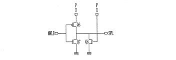
図2は図1のメインワードラインドライバの詳細回路図である。 FIG. 2 is a detailed circuit diagram of the main word line driver of FIG.
ワードラインイネーブル信号WLEがL(low)状態であれば、トランジスタQ1がターンオンされてノードK1はH(high)状態になる。インバータI1の出力はL状態なので、トランジスタQ5がターンオンされてノードK1の電位をラッチする。この際、インバータI2の出力はH状態なので、メインワードラインMWLBはイネーブルされなくなる。 If the word line enable signal WLE is in the L (low) state, the transistor Q1 is turned on and the node K1 is in the H (high) state. Since the output of inverter I1 is in the L state, transistor Q5 is turned on to latch the potential at node K1. At this time, since the output of the inverter I2 is in the H state, the main word line MWLB is not enabled.
ワードラインイネーブル信号WLEがH状態で、バンク選択アドレスをコーディングした信号(例えばBax34及びBax56)がH状態であれば、トランジスタQ1〜Q4がターンオンされるので、ノードK1の電位はL状態になる。したがって、インバータI2の出力はL状態になるので、メインワードラインMWLBがイネーブルされる。メインワードラインMWLBがL状態でイネーブルされると、図3に示したサブワードラインドライバのトランジスタQ6がターンオンされるので、PX信号PXによってサブワードラインSWLがH状態でイネーブルされる。メインワードラインMWLBがH状態であれば、トランジスタQ7がターンオンされるので、サブワードラインSWLはL状態でディスエーブルされる。トランジスタQ8のゲートに入力されるPX信号PXは、例えば1つのサブワードラインドライバを選択した場合、選択されていないサブワードラインドライバのフローティング状態を防ぐために使用される。 If the word line enable signal WLE is in the H state and the signals (for example, Bax34 and Bax56) coding the bank selection address are in the H state, the transistors Q1 to Q4 are turned on, so that the potential of the node K1 becomes the L state. Therefore, since the output of the inverter I2 is in the L state, the main word line MWLB is enabled. When the main word line MWLB is enabled in the L state, the transistor Q6 of the sub word line driver shown in FIG. 3 is turned on, so that the sub word line SWL is enabled in the H state by the PX signal PX. If the main word line MWLB is in the H state, the transistor Q7 is turned on, so that the sub word line SWL is disabled in the L state. The PX signal PX input to the gate of the transistor Q8 is used, for example, to prevent the unselected sub word line driver from floating when one sub word line driver is selected.
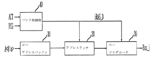
図4は従来の技術に係るメインローデコーダのブロック図である。 FIG. 4 is a block diagram of a main row decoder according to the prior art.
アドレス<0:n > がローアドレスバッファ10に入力される。アクティブ信号ACT及びフリチャージ信号PCGに応じて内部RAS信号iRAS_Dがバンク制御部40から生成される。ローアドレスバッファ10の出力は内部RAS信号iRAS_Dに応じてアドレスラッチ20にラッチされる。アドレスラッチ20の出力は内部RAS信号iRAS_Dに応じてローフリデコーダ30でフリデコードされる。 The address <0: n> is input to the row address buffer 10. An internal RAS signal iRAS_D is generated from the bank control unit 40 in response to the active signal ACT and the free charge signal PCG. The output of the row address buffer 10 is latched by the address latch 20 in response to the internal RAS signal iRAS_D. The output of the address latch 20 is subjected to free decoding by the row free decoder 30 in accordance with the internal RAS signal iRAS_D.
ローフリデコーダの出力Bax_jに応じてメインワードラインMWLBがイネーブルされる。 The main word line MWLB is enabled according to the output Bax_j of the row free decoder.
図5は図4のアドレスラッチ部の詳細回路図である。 FIG. 5 is a detailed circuit diagram of the address latch unit of FIG.
ローアドレスバッファ10の出力信号at_rowはインバータI5によって反転される。内部RAS信号iRAS_DはインバータI3によって反転され、インバータI3の出力はインバータI4によって反転される。インバータI7及びI8の詳細回路は四角ボックスに示されている。インバータI7及びI8は、イネーブルバー信号ENBがL状態でイネーブル信号ENがH状態のとき、インバータとして動作して入力信号を反転させる。インバータI5の出力は、インバータI3の出力がH状態でインバータI4の出力がL状態のとき、インバータI8によって反転される。インバータI8の出力は、インバータI3の出力がL状態でインバータI4の出力がH状態のとき、ラッチ500にラッチされる。ラッチ500の出力とインバータI3の出力はNORゲートG1で組み合わせられる。インバータI3の出力がH状態であれば、NORゲートG1の出力はラッチ500の出力に関係なくL状態になる。NORゲートG1の出力はインバータI5によって反転される。
The output signal at_row of the row address buffer 10 is inverted by the inverter I5. Internal RAS signal iRAS_D is inverted by inverter I3, and the output of inverter I3 is inverted by inverter I4. The detailed circuit of inverters I7 and I8 is shown in the square box. The inverters I7 and I8 operate as inverters and invert the input signal when the enable bar signal ENB is in the L state and the enable signal EN is in the H state. The output of inverter I5 is inverted by inverter I8 when the output of inverter I3 is in the H state and the output of inverter I4 is in the L state. The output of the inverter I8 is latched in the
上述した従来のメインローデコーダは、メインワードラインが選択され、それに連結されたサブワードラインが選択された状態でも、アクティブ又はフリチャージ信号に応じてメインワードラインがアクティブ又はフリチャージされてメインワードラインがトグルされる。 In the conventional main row decoder described above, even when a main word line is selected and a sub word line connected to the main word line is selected, the main word line is activated or precharged according to an active or precharge signal. Is toggled.
すなわち、図6に示したように、ローアドレスAx<j>によってサブワードラインが選択されても、サブワードラインのコーディングに関係なくメインローデコーダの出力、すなわちローフリデコーダの出力Bax_jが変わる度に、メインワードラインMWLBがアクティブ及びフリチャージ状態を反復するので、パワー消費が大きくなる。 That is, as shown in FIG. 6, even when a sub word line is selected by a row address Ax <j>, every time the output of the main row decoder, that is, the output Bax_j of the row free decoder changes, regardless of the coding of the sub word line, Since the main word line MWLB repeats the active and free charge states, power consumption increases.
したがって、本発明は、かかる問題点を解消するためのもので、その目的は、メインローデコーダの最下位ビットの状態変化を検出し、この最下位ビットの状態が変わるときのみメインワードラインがアクティブ又はフリチャージされるようにした半導体メモリ素子のメインローデコーダを提供することにある。 Therefore, the present invention is to solve such a problem, and its purpose is to detect a change in the state of the least significant bit of the main row decoder and to activate the main word line only when the state of the least significant bit changes. Another object of the present invention is to provide a main row decoder of a semiconductor memory device that is to be precharged.
上記目的を達成するための本発明に係る半導体メモリ素子のメインローデコーダは、アクティブ及びフリチャージ信号に応じて内部RAS信号を生成するためのバンク制御部と、前記内部RAS信号が遷移するとき、第1パルス信号を生成するための第1パルス発生回路と、前記内部RAS信号又はセルフリフレッシュ信号が遷移するとき、第2パルス信号を生成するための第2パルス発生回路と、前記第1パルス信号に応じてローアドレスの最下位ビットをラッチするためのアドレスラッチ部と、前記第2パルス信号に応じて前記ラッチ部の出力をデコードするためのフリデコーダとを含む。 To achieve the above object, the main row decoder of the semiconductor memory device according to the present invention includes a bank control unit for generating an internal RAS signal in response to an active and free charge signal, and when the internal RAS signal transitions. A first pulse generation circuit for generating a first pulse signal; a second pulse generation circuit for generating a second pulse signal when the internal RAS signal or self-refresh signal transitions; and the first pulse signal And an address latch unit for latching the least significant bit of the row address, and a free decoder for decoding the output of the latch unit according to the second pulse signal.
本発明によれば、メインワードラインがローアドレスの最下位ビットの状態が遷移するときのみトグルするので、メインワードラインのキャパシタにチャージ及びディスチャージされるVpp消耗電流を減らすことができる。 According to the present invention, since the main word line toggles only when the state of the least significant bit of the row address changes, it is possible to reduce the Vpp consumption current charged and discharged in the capacitor of the main word line.
また、本発明は、リフレッシュ動作のような一定の時間に全てのセルをリフレッシュするために順次ワードラインをイネーブルさせる場合に非常に効率的である。 Also, the present invention is very efficient when sequentially enabling word lines in order to refresh all cells at a certain time such as a refresh operation.
以下、添付図面を参照して本発明に係る実施例を詳細に説明する。 Hereinafter, embodiments according to the present invention will be described in detail with reference to the accompanying drawings.
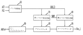
図7は本発明に係るメインローデコーダのブロック図である。 FIG. 7 is a block diagram of a main row decoder according to the present invention.
アドレス<0:n>がローアドレスバッファ60に入力される。アクティブ信号ACT及びフリチャージ信号PCGに応じて内部RAS信号iRAS_Dがバンク制御部40から生成される。
The address <0: n> is input to the
内部RAS信号iRAS_Dが変わる度に、第1パルス発生回路70から第1パルスSel_iRAS1が生成される。また、内部RAS信号iRAS_D又はセルフリフレッシュ信号SREFが遷移する度に第2パルス発生回路90から第2パルスSel_iRAS2が生成される。ローアドレスバッファ60の出力は第1パルスSel_iRAS1に応じてアドレスラッチ80にラッチされる。アドレスラッチ80の出力は第2パルスSel_iRAS2に応じてローフリデコーダ95でフリデコードされる。ローフリデコーダの出力Bax_jに応じてメインワードラインがイネーブルされる。
Each time the internal RAS signal iRAS_D changes, the first
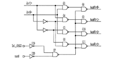
図8は図7の第1パルス発生回路の詳細回路図である。 FIG. 8 is a detailed circuit diagram of the first pulse generating circuit of FIG.
内部RAS信号iRAS_DはインバータI10によって反転される。インバータI10の出力は遅延部75で遅延される。遅延部75の出力はインバータI11によって反転される。インバータI10及びI11の出力はNORゲートG2によって組み合わせられる。NORゲートG2の出力が第1パルス信号Sel_iRAS1になり、インバータI12で反転された信号が、反転された第2パルスSel_iRAS1Bになる。
Internal RAS signal iRAS_D is inverted by inverter I10. The output of the inverter I10 is delayed by the
第1パルス発生回路70は、内部RAS信号が変わるときにパルスを発生させる。すなわち、インバータI10の出力がH状態であれば、NORゲートG2の出力はL状態になる。インバータI10の出力がL状態に変わると、インバータI10及びI11の出力が全てL状態なので、NORゲートG2の出力はH状態になる反面、インバータI12の出力はL状態になる。
The first
図9は図7のアドレスラッチ部の詳細回路図である。 FIG. 9 is a detailed circuit diagram of the address latch unit of FIG.
ローアドレスバッファ60の出力信号at_rowはインバータI13によって反転される。インバータI13の出力は第1パルスSel_iRAS1がH状態で、反転された第2パルスSel_iRAS1BがL状態のとき、インバータI14によって反転される。インバータI14の出力は、第1パルスSel_iRAS1がL状態で、反転された第2パルスSel_iRAS1BがH状態のとき、ラッチ800にラッチされる。ラッチ800の出力はインバータI17及びI18を経由し、インバータI18の出力Axは図7のローフリデコーダ95に入力される。
The output signal at_row of the
従来のアドレスラッチ部では、サブワードラインがコーディングされた状態でも、アクティブ又はフリチャージ信号が表示されると、メインワードラインがアクティブ又はフリチャージされた。ところが、本発明のアドレスラッチ部では、サブワードラインがコーディングされた状態でアクティブ又はフリチャージ信号が表示されても、ラッチに記憶されたローアドレスの最下位ビットをローフリデコーダに提供し、ローフリデコーダの出力によって、メインワードラインは以前状態をそのまま保つことができる。すなわち、ラッチ800に記憶された最下位ビットの状態が変わるときのみメインワードラインがアクティブ又はフリチャージされる。
In the conventional address latch unit, even when the sub word line is coded, when the active or free charge signal is displayed, the main word line is activated or free charged. However, the address latch unit of the present invention provides the low-free decoder with the least significant bit of the row address stored in the latch even if the active or precharge signal is displayed with the sub word line coded. The output of the decoder can keep the previous state of the main word line. That is, the main word line is activated or precharged only when the state of the least significant bit stored in the
図10は図7のローフリデコーダの詳細回路図である。 FIG. 10 is a detailed circuit diagram of the low-free decoder of FIG.
アドレスラッチ80の出力(例えばAx<0>及びAx<1>は、NANDゲートG3〜G6によってデコードされる。アドレスAx<1>は、2つのNANDゲートG3とG4に入力され、かつインバータI22を介して2つのNANDゲートG5及びG6に入力される。アドレスAx<0>は2つのNANDゲートG3とG5に入力され、かつインバータI21を介して2つのNANDゲートG4とG6に入力される。第2パルスSel_RAS2又はローアドレスイネーブル信号xaedがH状態であれば、インバータI19又はI20の出力がL状態になり、これによりNANDゲートG7の出力がH状態になる。したがって、NANDゲートG3〜G6の出力がNANDゲートG8〜G11によって反転される。NANDゲートG8〜G11の出力がバンクアドレスbax01<0>〜bax01<3>になる。これらのバンクアドレスbax01<0>〜bax01<3>によってメインワードラインが選択される。 Outputs of the address latch 80 (for example, Ax <0> and Ax <1> are decoded by NAND gates G3 to G6. The address Ax <1> is input to the two NAND gates G3 and G4, and the inverter I22 is connected. The address Ax <0> is input to the two NAND gates G3 and G5, and is input to the two NAND gates G4 and G6 via the inverter I21. If the 2-pulse Sel_RAS2 or the row address enable signal xaed is in the H state, the output of the inverter I19 or I20 is in the L state, thereby causing the output of the NAND gate G7 to be in the H state, and thus the outputs of the NAND gates G3 to G6. Are inverted by NAND gates G8 to G11. Output bank address Bax01 becomes <0> ~bax01 <3>. The main word line is selected by these bank addresses bax01 <0> ~bax01 <3>.
図11は本発明によってサブワードラインが選択される過程を説明するためのタイミング図である。 FIG. 11 is a timing diagram illustrating a process of selecting a sub word line according to the present invention.
ローアドレスAx<j>の最下位ビットがL状態からH状態に遷移する場合、このH状態をアドレスラッチ80によってラッチする。ローフリデコーダ95の出力Bax_j[n−1]はH状態からL状態に遷移する。ローフリデコーダ95の出力Bax_j[n]はL状態からH状態に遷移する。ローフリデコーダ95の出力Bax_j[n+1]はL状態を保つ。したがって、メインワードラインMWLB[k]はL状態からH状態に遷移し、メインワードライン[k+1]はH状態を保つ。したがって、サブワードラインSWLはアクティブACT時毎にH状態でイネーブルされる。
When the least significant bit of the row address Ax <j> transitions from the L state to the H state, the H state is latched by the
アドレスラッチ80にラッチされたローアドレスAx<j>の最下位ビットが変わる場合(例えば、H状態からL状態へ)、このH状態をアドレスラッチ80によってラッチする。ローフリデコーダ95の出力Bax_j[n−1]はL状態を保つ。ローフリデコーダ95の出力Bax_j[n]はH状態からL状態に遷移する。ローフリデコーダ95の出力Bax_j[n+1]はL状態からH状態に遷移する。したがって、メインワードラインMWLB[k]は、L状態からH状態に遷移し、メインワードラインMWLB[k+1]はH状態からL状態に遷移する。すなわち、ローアドレスの最下位ビットが変わる場合にのみメインワードラインがトグルされるので、メインワードラインのキャパシタにチャージ及びディスチャージされるVpp消耗電流を減らすことができる。
When the least significant bit of the row address Ax <j> latched in the
メインワードラインをVppを用いて1回アクティブ及びフリチャージするときに消耗される電流i=C(メインワードラインのキャパシタ)×Vpp/tになる。 The current consumed when the main word line is activated and precharged once using Vpp is i = C (capacitor of main word line) × Vpp / t.
例えば、8つのサブワードラインドライバのワードラインを順次イネーブルするに消耗される電流を計算する。 For example, the current consumed to sequentially enable the word lines of the eight sub word line drivers is calculated.
従来の場合には、消耗される電流I=8(サブワードラインの数)*2(アクティブ及びフリチャージ)×i(メインワードラインをVppを用いてアクティブ及びフリチャージするときに消耗される電流)になる。 In the conventional case, consumed current I = 8 (number of sub word lines) * 2 (active and free charge) × i (current consumed when main word line is activated and free charged using Vpp) become.
これに対し、本発明の場合には、I=1*2(最初のアクティブ及び最後のフリチャージ)×i(メインワードラインをVppを用いてアクティブ及びフリチャージするときに消耗される電流)になる。 In contrast, in the present invention, I = 1 * 2 (first active and last free charge) × i (current consumed when the main word line is activated and free charged using Vpp). Become.
したがって、本発明によれば、従来より消耗電流を1/8に減少させることができる。 Therefore, according to the present invention, the consumption current can be reduced to 1/8 compared with the conventional case.
50 バンク制御部
60 ローアドレスバッファ
70 第1パルス発生回路
80 アドレスラッチ
90 第2パルス発生回路
95 ローフリデコーダ
50
Claims (8)
前記内部RAS信号が遷移するとき、第1パルス信号を生成するための第1パルス発生回路と、
前記内部RAS信号又はセルフリフレッシュ信号が遷移するとき、第2パルス信号を生成するための第2パルス発生回路と、
前記第1パルス信号に応じてローアドレスの最下位ビットをラッチするためのアドレスラッチ部と、
前記第2パルス信号に応じて前記ラッチ部の出力をデコードするためのフリデコーダとを含む半導体メモリ素子のメインローフリデコーダ。 A bank controller for generating an internal RAS signal in response to the active and free charge signals;
A first pulse generating circuit for generating a first pulse signal when the internal RAS signal transitions;
A second pulse generation circuit for generating a second pulse signal when the internal RAS signal or the self-refresh signal transits;
An address latch unit for latching the least significant bit of the row address according to the first pulse signal;
A main row free decoder of a semiconductor memory device, comprising: a free decoder for decoding an output of the latch unit according to the second pulse signal.
前記第3インバータの出力を反転させるための第4インバータとをさらに含むことを特徴とする請求項1記載の半導体メモリ素子のメインローデコーダ。 A third inverter for inverting the output of the latch;
The main row decoder of claim 1, further comprising a fourth inverter for inverting the output of the third inverter.
前記第1インバータの出力を遅延させるための遅延部と、
前記遅延部の出力を反転させるための第2インバータと、
前記第1及び第2インバータの出力を論理的に組み合わせるためのNORゲートとを含むことを特徴とする請求項2記載の半導体素子のメインローデコーダ。
A first inverter for inverting the internal RAS signal;
A delay unit for delaying the output of the first inverter;
A second inverter for inverting the output of the delay unit;
3. The main row decoder for a semiconductor device according to claim 2, further comprising a NOR gate for logically combining the outputs of the first and second inverters.
Applications Claiming Priority (2)
| Application Number | Priority Date | Filing Date | Title |
|---|---|---|---|
| KR1020030100161A KR100593145B1 (en) | 2003-12-30 | 2003-12-30 | Main row decoder in a semiconductor memory device |
| KR2003-100161 | 2003-12-30 |
Publications (2)
| Publication Number | Publication Date |
|---|---|
| JP2005196933A true JP2005196933A (en) | 2005-07-21 |
| JP5115913B2 JP5115913B2 (en) | 2013-01-09 |
Family
ID=34698737
Family Applications (1)
| Application Number | Title | Priority Date | Filing Date |
|---|---|---|---|
| JP2004194318A Expired - Fee Related JP5115913B2 (en) | 2003-12-30 | 2004-06-30 | Main row decoder for semiconductor memory device |
Country Status (3)
| Country | Link |
|---|---|
| US (1) | US6973007B2 (en) |
| JP (1) | JP5115913B2 (en) |
| KR (1) | KR100593145B1 (en) |
Families Citing this family (5)
| Publication number | Priority date | Publication date | Assignee | Title |
|---|---|---|---|---|
| KR100543914B1 (en) * | 2003-04-30 | 2006-01-23 | 주식회사 하이닉스반도체 | Semiconductor memory device for reducing peak current during refreshing operation |
| KR100688513B1 (en) * | 2005-01-05 | 2007-03-02 | 삼성전자주식회사 | Boosted voltage generating circuit and method in semiconductor memory device |
| KR100666173B1 (en) * | 2005-02-04 | 2007-01-09 | 삼성전자주식회사 | Semiconductor memory device having negatively controlled sub wordline scheme and operating method for the same |
| KR100706830B1 (en) * | 2005-10-19 | 2007-04-13 | 주식회사 하이닉스반도체 | Apparatus and method for controlling active period of semiconductor memory |
| KR100656445B1 (en) * | 2005-11-29 | 2006-12-11 | 주식회사 하이닉스반도체 | Circuit for inputting address in semiconductor memory apparatus |
Citations (7)
| Publication number | Priority date | Publication date | Assignee | Title |
|---|---|---|---|---|
| JPH04209392A (en) * | 1990-11-30 | 1992-07-30 | Nec Corp | Semiconductor storage device |
| JPH1116348A (en) * | 1997-06-25 | 1999-01-22 | Hitachi Ltd | Semiconductor memory device |
| JPH11195294A (en) * | 1997-12-27 | 1999-07-21 | Samsung Electron Co Ltd | Address decoding device for semiconductor memory |
| JP2000048558A (en) * | 1998-05-22 | 2000-02-18 | Mitsubishi Electric Corp | Semiconductor memory device |
| JP2000099398A (en) * | 1998-09-22 | 2000-04-07 | Fujitsu Ltd | Electronic device, semiconductor storage device, bus master and semiconductor storage device accessing method |
| JP2000132968A (en) * | 1998-10-28 | 2000-05-12 | Hitachi Ltd | Semiconductor integrated circuit device |
| JP2002184182A (en) * | 2000-10-05 | 2002-06-28 | Fujitsu Ltd | Semiconductor memory and its control method |
Family Cites Families (5)
| Publication number | Priority date | Publication date | Assignee | Title |
|---|---|---|---|---|
| JPH09288614A (en) * | 1996-04-22 | 1997-11-04 | Mitsubishi Electric Corp | Semiconductor integrated circuit device, semiconductor storage device and control circuit therefor |
| JP2001060392A (en) * | 1999-08-24 | 2001-03-06 | Mitsubishi Electric Corp | Semiconductor device |
| JP4531892B2 (en) * | 1999-10-29 | 2010-08-25 | 富士通セミコンダクター株式会社 | Semiconductor integrated circuit, control method for semiconductor integrated circuit, and variable delay circuit |
| JP2002015570A (en) * | 2000-06-28 | 2002-01-18 | Toshiba Corp | Semiconductor memory |
| US6674684B1 (en) * | 2003-06-11 | 2004-01-06 | Infineon Technologies North America Corp. | Multi-bank chip compatible with a controller designed for a lesser number of banks and method of operating |
-
2003
- 2003-12-30 KR KR1020030100161A patent/KR100593145B1/en not_active IP Right Cessation
-
2004
- 2004-06-28 US US10/878,903 patent/US6973007B2/en not_active Expired - Fee Related
- 2004-06-30 JP JP2004194318A patent/JP5115913B2/en not_active Expired - Fee Related
Patent Citations (7)
| Publication number | Priority date | Publication date | Assignee | Title |
|---|---|---|---|---|
| JPH04209392A (en) * | 1990-11-30 | 1992-07-30 | Nec Corp | Semiconductor storage device |
| JPH1116348A (en) * | 1997-06-25 | 1999-01-22 | Hitachi Ltd | Semiconductor memory device |
| JPH11195294A (en) * | 1997-12-27 | 1999-07-21 | Samsung Electron Co Ltd | Address decoding device for semiconductor memory |
| JP2000048558A (en) * | 1998-05-22 | 2000-02-18 | Mitsubishi Electric Corp | Semiconductor memory device |
| JP2000099398A (en) * | 1998-09-22 | 2000-04-07 | Fujitsu Ltd | Electronic device, semiconductor storage device, bus master and semiconductor storage device accessing method |
| JP2000132968A (en) * | 1998-10-28 | 2000-05-12 | Hitachi Ltd | Semiconductor integrated circuit device |
| JP2002184182A (en) * | 2000-10-05 | 2002-06-28 | Fujitsu Ltd | Semiconductor memory and its control method |
Also Published As
| Publication number | Publication date |
|---|---|
| US20050141326A1 (en) | 2005-06-30 |
| US6973007B2 (en) | 2005-12-06 |
| KR20050068578A (en) | 2005-07-05 |
| KR100593145B1 (en) | 2006-06-26 |
| JP5115913B2 (en) | 2013-01-09 |
Similar Documents
| Publication | Publication Date | Title |
|---|---|---|
| US6504783B2 (en) | Semiconductor device having early operation high voltage generator and high voltage supplying method therefor | |
| KR100772110B1 (en) | Row address controller | |
| JPH07111084A (en) | Semiconductor integrated circuit device | |
| JPH10188562A (en) | Refreshing circuit of semiconductor memory and method therefor | |
| JPH02177196A (en) | Static semiconductor memory | |
| JP2008269772A (en) | Column redundancy circuit | |
| JP2006120301A (en) | Leakage current control device of semiconductor memory device | |
| US20040093461A1 (en) | Self-refresh device and method | |
| US7027351B2 (en) | Negative word line driver | |
| JP2007273007A (en) | Semiconductor memory device | |
| JP3751740B2 (en) | Isolation gate control method and circuit for semiconductor memory device | |
| US7426151B2 (en) | Device and method for performing a partial array refresh operation | |
| JP5115913B2 (en) | Main row decoder for semiconductor memory device | |
| US6930952B2 (en) | Method of reading memory device in page mode and row decoder control circuit using the same | |
| JP2008165956A (en) | Semiconductor memory device for selectively driving negative word line | |
| KR100384559B1 (en) | Column decoding apparatus of semiconductor memory device | |
| JP2004127440A (en) | Multi-port memory circuit | |
| TW201830397A (en) | Circuit and method for writing to a bit cell | |
| JP2000030451A (en) | Semiconductor memory device and its column decoder | |
| JP2805467B2 (en) | Low power consumption DRAM bit line selection circuit | |
| JP2004171744A (en) | Semiconductor memory device and method for arranging the same | |
| KR20080040207A (en) | Semiconductor memory device | |
| US6473347B2 (en) | Semiconductor device having memory with effective precharging scheme | |
| JP2006059490A (en) | Semiconductor memory | |
| US20220189542A1 (en) | Circuit and method of writing to a bit cell |
Legal Events
| Date | Code | Title | Description |
|---|---|---|---|
| A621 | Written request for application examination |
Free format text: JAPANESE INTERMEDIATE CODE: A621 Effective date: 20061114 |
|
| A977 | Report on retrieval |
Free format text: JAPANESE INTERMEDIATE CODE: A971007 Effective date: 20091014 |
|
| A131 | Notification of reasons for refusal |
Free format text: JAPANESE INTERMEDIATE CODE: A131 Effective date: 20091020 |
|
| A601 | Written request for extension of time |
Free format text: JAPANESE INTERMEDIATE CODE: A601 Effective date: 20100120 |
|
| A602 | Written permission of extension of time |
Free format text: JAPANESE INTERMEDIATE CODE: A602 Effective date: 20100125 |
|
| A521 | Written amendment |
Free format text: JAPANESE INTERMEDIATE CODE: A523 Effective date: 20100219 |
|
| A131 | Notification of reasons for refusal |
Free format text: JAPANESE INTERMEDIATE CODE: A131 Effective date: 20101102 |
|
| A521 | Written amendment |
Free format text: JAPANESE INTERMEDIATE CODE: A523 Effective date: 20110201 |
|
| A131 | Notification of reasons for refusal |
Free format text: JAPANESE INTERMEDIATE CODE: A131 Effective date: 20111108 |
|
| A601 | Written request for extension of time |
Free format text: JAPANESE INTERMEDIATE CODE: A601 Effective date: 20120208 |
|
| A602 | Written permission of extension of time |
Free format text: JAPANESE INTERMEDIATE CODE: A602 Effective date: 20120213 |
|
| A521 | Written amendment |
Free format text: JAPANESE INTERMEDIATE CODE: A523 Effective date: 20120308 |
|
| A02 | Decision of refusal |
Free format text: JAPANESE INTERMEDIATE CODE: A02 Effective date: 20120403 |
|
| RD03 | Notification of appointment of power of attorney |
Free format text: JAPANESE INTERMEDIATE CODE: A7423 Effective date: 20120424 |
|
| A521 | Written amendment |
Free format text: JAPANESE INTERMEDIATE CODE: A523 Effective date: 20120803 |
|
| A911 | Transfer to examiner for re-examination before appeal (zenchi) |
Free format text: JAPANESE INTERMEDIATE CODE: A911 Effective date: 20120810 |
|
| TRDD | Decision of grant or rejection written | ||
| A01 | Written decision to grant a patent or to grant a registration (utility model) |
Free format text: JAPANESE INTERMEDIATE CODE: A01 Effective date: 20120911 |
|
| A01 | Written decision to grant a patent or to grant a registration (utility model) |
Free format text: JAPANESE INTERMEDIATE CODE: A01 |
|
| A61 | First payment of annual fees (during grant procedure) |
Free format text: JAPANESE INTERMEDIATE CODE: A61 Effective date: 20121009 |
|
| R150 | Certificate of patent or registration of utility model |
Free format text: JAPANESE INTERMEDIATE CODE: R150 |
|
| FPAY | Renewal fee payment (event date is renewal date of database) |
Free format text: PAYMENT UNTIL: 20151026 Year of fee payment: 3 |
|
| LAPS | Cancellation because of no payment of annual fees |