JP2005159595A - Projection video display apparatus - Google Patents
Projection video display apparatus Download PDFInfo
- Publication number
- JP2005159595A JP2005159595A JP2003393401A JP2003393401A JP2005159595A JP 2005159595 A JP2005159595 A JP 2005159595A JP 2003393401 A JP2003393401 A JP 2003393401A JP 2003393401 A JP2003393401 A JP 2003393401A JP 2005159595 A JP2005159595 A JP 2005159595A
- Authority
- JP
- Japan
- Prior art keywords
- lamp
- lamp power
- light source
- data
- video signal
- Prior art date
- Legal status (The legal status is an assumption and is not a legal conclusion. Google has not performed a legal analysis and makes no representation as to the accuracy of the status listed.)
- Granted
Links
- 230000002123 temporal effect Effects 0.000 claims description 2
- 238000005286 illumination Methods 0.000 abstract description 4
- 230000000007 visual effect Effects 0.000 abstract description 2
- 238000004364 calculation method Methods 0.000 description 7
- 238000013500 data storage Methods 0.000 description 5
- 239000004973 liquid crystal related substance Substances 0.000 description 5
- 238000006243 chemical reaction Methods 0.000 description 3
- 206010052143 Ocular discomfort Diseases 0.000 description 2
- 238000010586 diagram Methods 0.000 description 2
- 238000007796 conventional method Methods 0.000 description 1
- 238000001514 detection method Methods 0.000 description 1
- 238000000034 method Methods 0.000 description 1
- 230000007704 transition Effects 0.000 description 1
Images
Landscapes
- Control Of Indicators Other Than Cathode Ray Tubes (AREA)
- Projection Apparatus (AREA)
- Liquid Crystal Display Device Control (AREA)
- Transforming Electric Information Into Light Information (AREA)
Abstract
Description
この発明は、LCD、DLP等の投射型映像表示装置に関する。 The present invention relates to a projection-type image display device such as an LCD or DLP.
LCD、DLP等のデバイスをライトバルブとして利用して画像を表示する投射型映像表示装置において、入力された映像信号の平均輝度レベル(APL)を検出し、検出された平均輝度レベルが高いほど光源ランプの照度が高くなるように、光源ランプの照度を制御する方法が既に開発されている(特開平03−179886号公報、特開平08−201812号公報参照)。 In a projection-type video display device that displays an image by using a device such as an LCD or DLP as a light valve, an average luminance level (APL) of an input video signal is detected, and a light source increases as the detected average luminance level increases. A method of controlling the illuminance of the light source lamp has been developed so that the illuminance of the lamp is increased (see Japanese Patent Laid-Open Nos. 03-179886 and 08-201812).
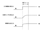
従来方法では、次のような問題がある。つまり、図1に示すように、映像信号の平均輝度レベルがシーンチェンジなどで大きく変化した場合、光源ランプの電力制御信号はその検出結果に対応して即座に変化せしめられるが、実際に光源ランプの照度が切り替わるまでには、電力を供給するランプバラストの出力特性と光源ランプ自体の応答特性によって、数フレーム分の時間がかかってしまう。 The conventional method has the following problems. That is, as shown in FIG. 1, when the average luminance level of the video signal changes greatly due to a scene change or the like, the power control signal of the light source lamp is immediately changed according to the detection result. It takes time for several frames until the illuminance is switched due to the output characteristics of the lamp ballast that supplies power and the response characteristics of the light source lamp itself.
この遅延時間は視覚的に十分認知できる長さであるため、たとえば、画像の内容が「暗い」から「明るい」と変化した場合、視覚的には、「暗い」、「中間」、「明るい」という変化と感じられ、違和感が発生する。
この発明は、入力された映像信号の明るさに関する情報に基づいて、光源ランプの照度が制御される投射型映像表示装置において、入力された映像信号の明るさが大きく変化した場合に、光源ランプの応答遅れによって発生する視覚的な違和感を低減させることができる投射型映像表示装置を提供することを目的とする。 The present invention provides a projection-type video display apparatus in which the illuminance of a light source lamp is controlled based on information on the brightness of an input video signal, and when the brightness of the input video signal changes greatly, It is an object of the present invention to provide a projection display apparatus that can reduce the visual discomfort caused by the response delay.
請求項1に記載の発明は、光源ランプ、光源ランプの光の強度を変調することによって画像を表示するライトバルブ、入力された画像の明るさに関する情報を算出する手段、および画像の明るさに関する情報に基づいて、ランプ電力を制御することにより、光源の照度を制御する手段とを備えている投射型映像表示装置において、現フレームに対するランプ電力に関するデータと、過去の所定数のフレーム分に対するランプ電力に関するデータとに基づいて、入力映像信号の信号レベルを変化させる信号レベル変調手段を備えていることを特徴とする。
The invention described in
請求項2に記載の発明は、請求項1に記載の発明において、信号レベル変調手段は、現フレームに対するランプ電力に関するデータと、過去の所定数のフレーム分に対するランプ電力に関するデータとが、それぞれ入力され、かつ入力されたランプ電力に関するデータに所与の乗算係数を乗算する複数の乗算手段、ランプ電力に関するデータの時間的変化量に基づいて、各乗算手段に設定される乗算係数を切り換える手段、各乗算手段の乗算結果に基づいて、入力映像信号の信号レベルのゲイン差分値を算出する手段、算出されたゲイン差分値を基準となるゲインに加算することによりゲインを算出し、算出したゲインに応じて入力映像信号の信号レベルを変化させる手段を備えていることを特徴とする。 According to a second aspect of the present invention, in the first aspect of the invention, the signal level modulation means inputs data relating to the lamp power for the current frame and data relating to the lamp power for a predetermined number of frames in the past. A plurality of multiplying means for multiplying the input data relating to lamp power by a given multiplication coefficient, and means for switching the multiplication coefficient set in each multiplication means based on the amount of temporal change in the data relating to lamp power; Based on the multiplication result of each multiplication means, means for calculating the gain difference value of the signal level of the input video signal, calculating the gain by adding the calculated gain difference value to the reference gain, and calculating the gain In accordance with this, there is provided means for changing the signal level of the input video signal.
この発明によれば、入力された映像信号の明るさに関する情報に基づいて、光源ランプの照度が制御される投射型映像表示装置において、入力された映像信号の明るさが大きく変化した場合に、光源ランプの応答遅れによって発生する視覚的な違和感を低減させることができるようになる。 According to the present invention, in the projection-type video display device in which the illuminance of the light source lamp is controlled based on the information related to the brightness of the input video signal, when the brightness of the input video signal changes greatly, Visual discomfort caused by a response delay of the light source lamp can be reduced.
以下、図面を参照して、この発明を液晶プロジェクタに適用した場合の実施例について説明する。 Embodiments in which the present invention is applied to a liquid crystal projector will be described below with reference to the drawings.
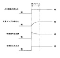
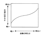
まず、図2を用いて、本発明の原理について説明する。図2に示すように、入力画像の明るさが「暗い」から「明るい」に変化した場合、光源ランプの電力が大きくされる。これにより、光源ランプの照度が高く(明るく)なるように変化するが、図2に示すように、光源ランプの応答特性により、光源ランプの照度が入力画像の明るさに対応する照度に至るまでに時間がかかる。 First, the principle of the present invention will be described with reference to FIG. As shown in FIG. 2, when the brightness of the input image changes from “dark” to “bright”, the power of the light source lamp is increased. As a result, the illuminance of the light source lamp changes so as to become high (bright). However, as shown in FIG. 2, the illuminance of the light source lamp reaches the illuminance corresponding to the brightness of the input image due to the response characteristics of the light source lamp. Takes time.
そこで、本願発明では、図2に示すように、入力画像の明るさが「暗い」から「明るい」に変化したときから、光源ランプの照度が入力画像の明るさに対応する照度に至るまでの過渡期間において、入力映像信号のレベルを持ち上げることにより、視覚的な見え方が「暗い」から「明るい」に変化するようにしている。 Therefore, in the present invention, as shown in FIG. 2, from when the brightness of the input image changes from “dark” to “bright”, the illuminance of the light source lamp reaches the illuminance corresponding to the brightness of the input image. During the transition period, the visual appearance changes from “dark” to “bright” by raising the level of the input video signal.
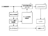
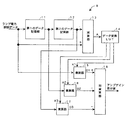
図3は、液晶プロジェクタの構成を示している。 FIG. 3 shows the configuration of the liquid crystal projector.
液晶プロジェクタに入力された映像信号(R,G,B信号)は、信号変調処理部(アンプ)1およびLCDドライバ2を介してLCD3に送られる。LCD3に書き込まれた画像は、光源ランプ7によって、図示しないスクリーン上に投射される。
Video signals (R, G, B signals) input to the liquid crystal projector are sent to the
また、液晶プロジェクタに入力された映像信号は、入力画像の明るさに関する情報を算出するための明るさ判定部4にも送られる。入力画像の明るさに関する情報としては、1画面全体の平均輝度レベル(APL)、1画面全体の輝度の総和、1画面中の最大輝度レベル(ピーク値)、1画面中の最小輝度レベル等が用いられる。また、1画面を複数のエリアに分割して、エリア毎の平均輝度レベルをヒストグラム化し、最も度数の高い輝度を入力画像の明るさに関する情報として用いてもよい。 The video signal input to the liquid crystal projector is also sent to the brightness determination unit 4 for calculating information related to the brightness of the input image. Information on the brightness of the input image includes the average luminance level (APL) of the entire screen, the total luminance of the entire screen, the maximum luminance level (peak value) in the screen, the minimum luminance level in the screen, and the like. Used. Alternatively, one screen may be divided into a plurality of areas, the average luminance level for each area may be histogrammed, and the highest luminance may be used as information regarding the brightness of the input image.
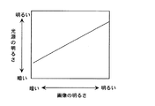
この実施例では、明るさ判定部4は、1画面(この例では1フレーム)毎に平均輝度レベル(APL)を算出する。明るさ判定部4によって算出された平均輝度レベルは、ランプ電力制御部5に送られる。ランプ電力制御部5は、明るさ判定部4から送られてきた平均輝度レベルが高いほど、光源ランプ7の照度が高くなるように、ランプ電力を制御する。入力映像信号の平均輝度レベルと、光源ランプ7の照度(ランプ電力)との関係は、図4に示すように線形的な関係に設定してもよいし、図5に示すように非線形な関係に設定してもよい。
In this embodiment, the brightness determination unit 4 calculates an average luminance level (APL) for each screen (one frame in this example). The average luminance level calculated by the brightness determination unit 4 is sent to the lamp
ランプ電力制御部5からは、ランプ電力に比例したランプ電力制御データ(ランプ電力に関するデータ)が出力される。ランプ電力制御部5から出力されるランプ電力制御データは、ランブバラスト6に送られる。ランブバラスト6は、ランプ電力制御部5から送られてくるランプ電力制御データに応じて、光源ランプ7のランプ電力を制御する。
The lamp
ランプ電力制御部5から出力されるランプ電力制御データは、信号変調処理部(アンプ)1のアンプゲインを制御するためのフィルタ処理回路部8にも送られる。
The lamp power control data output from the lamp
図6は、フィルタ処理回路部8の構成を示している。
FIG. 6 shows the configuration of the filter
図6において、11は1フレーム前のランプ電力制御データを記憶するための第1のデータ記憶部であり、12は2フレーム前のランプ電力制御データを記憶するための第2のデータ記憶部である。ランプ電力制御データとしては、ランプ電力をそのまま表すデータであってもよいし、演算により8段階(3bit)や16段階(4bit)などの形式のデータであってもよい。 In FIG. 6, 11 is a first data storage unit for storing lamp power control data for the previous frame, and 12 is a second data storage unit for storing lamp power control data for the previous frame. is there. The lamp power control data may be data representing the lamp power as it is, or may be data in a format such as 8 stages (3 bits) or 16 stages (4 bits) by calculation.
現フレームのランプ電力制御データと、第2のデータ記憶部12に記憶されている2フレーム前のランプ電力制御データとは、減算器13に与えられる。減算器13は、現フレームのランプ電力制御データから、2フレーム前のランプ電力制御データとを減算し、その演算結果Aをデータ変換LUT14に与える。
The lamp power control data of the current frame and the lamp power control data of two frames before stored in the second data storage unit 12 are given to the
一方、現フレームのランプ電力制御データは第1の乗算器15に、第1のデータ記憶部11に記憶されている1フレーム前のランプ電力制御データは第2の乗算器16に、第2のデータ記憶部12に記憶されている2フレーム前のランプ電力制御データは第3の乗算器17に、それぞれ与えられる。
On the other hand, the lamp power control data of the current frame is stored in the first multiplier 15, and the lamp power control data of the previous frame stored in the first data storage unit 11 is stored in the
第1〜第3の各乗算器15、16、17には、それぞれデータ変換LUT14によって、乗算係数K1,K2,K3が設定される。各乗算器15、16、17は、それぞれ入力データに、乗算係数K1,K2,K3を乗算する。各乗算器15、16、17の乗算結果D1,D2,D3は、加減算器18に与えられる。加減算器18は、(D1−D2−D3)の演算を行い、その演算結果をアンプゲイン差分値(入力映像信号の信号レベルの変調度合い)として出力する。アンプゲイン差分値は、信号変調処理部1に与えられる。信号変調処理部1は、与えられたアンプゲイン差分値を基準となるアンプゲイン設定値(デフォルト値)に加算することにより、アンプゲインを決定し、決定したアンプゲインに応じて入力映像信号の信号レベルを変化(変調)させる。
Multiplication coefficients K1, K2, and K3 are set in the first to
データ変換LUT14は、減算器13から与えられる演算結果Aに基づいて、第1〜第3の各乗算器15、16、17に設定する乗算係数K1,K2,K3を切り換える。K1,K2,K3は、所定の閾値をTHとすると、演算結果Aの値に応じて、次のような値に設定される。
The
(a)|A|<THの場合
K1=K2=K3=0
(b)|A|≧THでかつA≧0の場合
K1=1.0,K2=0.5,K3=0.5
(c)|A|≧THでかつA<0の場合
K1=1.0,K2=1.0,K3=0
(A) When | A | <TH K1 = K2 = K3 = 0
(B) When | A | ≧ TH and A ≧ 0 K1 = 1.0, K2 = 0.5, K3 = 0.5
(C) When | A | ≧ TH and A <0 K1 = 1.0, K2 = 1.0, K3 = 0
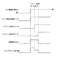
図7は、入力画像の明るさが「暗い」から「明るい」に変化したとき、つまり、平均輝度レベルが小さな値から大きな値に変化したときの、フィルタ処理回路部8の各部の信号(データ)を示している。
FIG. 7 shows signals (data) of each part of the filter
入力画像の明るさが「暗い」から「明るい」に変化すると、ランプ電力制御データも同様に変化せしめられる。この場合、1フレーム前のランプ電力制御データおよび2フレーム前のランプ電力制御データは、図7に示すようになるので、減算器13の演算結果A、つまり、現フレームのランプ電力制御データから2フレーム前のランプ電力制御データとを減算した結果は、図7に示すようになる。
When the brightness of the input image changes from “dark” to “bright”, the lamp power control data is similarly changed. In this case, the lamp power control data of the previous frame and the lamp power control data of the previous frame are as shown in FIG. 7, and therefore, 2 from the calculation result A of the
入力画像の明るさが「暗い」から「明るい」に変化してから2フレーム期間においては、|A|≧THでかつA≧0となるので、その期間において、各乗算器15、16、17に設定する乗算係数K1,K2,K3は、K1=1.0,K2=0.5,K3=0.5となる。したがって、加減算器18によって算出されるアンプゲイン差分値は、図7に示すように、入力画像の明るさが「暗い」から「明るい」に変化してから最初の1フレーム期間においては正の比較的大きな値となり、その次の1フレーム期間においては正の比較的小さな値となる。この結果、その期間において、入力映像信号のレベルは、図2で説明したように、持ち上げられるので、光源ランプ7の応答の遅れを補うことができるようになる。
In the two-frame period after the brightness of the input image changes from “dark” to “bright”, | A | ≧ TH and A ≧ 0. Therefore, in that period, each
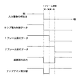
図8は、入力画像の明るさが「明るい」から「暗い」に変化したとき、つまり、平均輝度レベルが大きな値から小さな値に変化したときの、フィルタ処理回路部8の各部の信号(データ)を示している。
FIG. 8 shows signals (data) of each part of the filter
入力画像の明るさが「明るい」から「暗い」に変化すると、ランプ電力制御データも同様に変化せしめられる。この場合、1フレーム前のランプ電力制御データおよび2フレーム前のランプ電力制御データは、図8に示すようになるので、減算器13の演算結果A、つまり、現フレームのランプ電力制御データから2フレーム前のランプ電力制御データとを減算した結果は、図8に示すようになる。
When the brightness of the input image changes from “bright” to “dark”, the lamp power control data is similarly changed. In this case, the lamp power control data for the previous frame and the lamp power control data for the previous two frames are as shown in FIG. 8, and therefore, 2 from the calculation result A of the
入力画像の明るさが「明るい」から「暗い」に変化してから2フレーム期間においては、|A|≧THでかつA<0となるので、その期間において、各乗算器15、16、17に設定する乗算係数K1,K2,K3は、K1=1.0,K2=1.0,K3=0となる。したがって、加減算器18によって算出されるアンプゲイン差分値は、入力画像の明るさが「明るい」から「暗い」に変化してから最初の1フレーム期間において、図8に示すように、負の値となる。この結果、入力映像信号のレベルは、「明るい」から「暗い」に変化してから最初の1フレーム期間において低下せしめられるので、光源ランプ7の応答の遅れを補うことができるようになる。
Since | A | ≧ TH and A <0 in the two-frame period after the brightness of the input image changes from “bright” to “dark”, each
1 信号変調処理部(アンプ)
2 LCDドライバ
3 LCD
4 明るさ判定部
5 ランプ電力制御部
6 ランブバラスト
7 光源ランプ
8 フィルタ処理回路部
1 Signal modulation processing unit (amplifier)
2
4
Claims (2)
現フレームに対するランプ電力に関するデータと、過去の所定数のフレーム分に対するランプ電力に関するデータとに基づいて、入力映像信号の信号レベルを変化させる信号レベル変調手段を備えていることを特徴とする投射型映像表示装置。 Light source lamp, light valve that displays image by modulating light intensity of light source lamp, means for calculating information about brightness of input image, and control of lamp power based on information about brightness of image In the projection type video display device comprising a means for controlling the illuminance of the light source,
Projection type comprising signal level modulation means for changing the signal level of an input video signal based on data on lamp power for the current frame and data on lamp power for a predetermined number of frames in the past Video display device.
Priority Applications (1)
| Application Number | Priority Date | Filing Date | Title |
|---|---|---|---|
| JP2003393401A JP4530650B2 (en) | 2003-11-25 | 2003-11-25 | Projection-type image display device |
Applications Claiming Priority (1)
| Application Number | Priority Date | Filing Date | Title |
|---|---|---|---|
| JP2003393401A JP4530650B2 (en) | 2003-11-25 | 2003-11-25 | Projection-type image display device |
Publications (2)
| Publication Number | Publication Date |
|---|---|
| JP2005159595A true JP2005159595A (en) | 2005-06-16 |
| JP4530650B2 JP4530650B2 (en) | 2010-08-25 |
Family
ID=34719770
Family Applications (1)
| Application Number | Title | Priority Date | Filing Date |
|---|---|---|---|
| JP2003393401A Expired - Fee Related JP4530650B2 (en) | 2003-11-25 | 2003-11-25 | Projection-type image display device |
Country Status (1)
| Country | Link |
|---|---|
| JP (1) | JP4530650B2 (en) |
Cited By (3)
| Publication number | Priority date | Publication date | Assignee | Title |
|---|---|---|---|---|
| JP2007178987A (en) * | 2005-12-28 | 2007-07-12 | Lg Philips Lcd Co Ltd | Driving device and driving method of liquid crystal display element |
| JP2007322881A (en) * | 2006-06-02 | 2007-12-13 | Sony Corp | Display device and display control method |
| JP2010066714A (en) * | 2008-09-12 | 2010-03-25 | Sharp Corp | Liquid crystal display and led backlight control method for the liquid crystal display |
Citations (2)
| Publication number | Priority date | Publication date | Assignee | Title |
|---|---|---|---|---|
| JP2003036063A (en) * | 2001-04-25 | 2003-02-07 | Matsushita Electric Ind Co Ltd | Video display device and video display method |
| WO2003075257A1 (en) * | 2002-03-07 | 2003-09-12 | Sharp Kabushiki Kaisha | Display apparatus |
-
2003
- 2003-11-25 JP JP2003393401A patent/JP4530650B2/en not_active Expired - Fee Related
Patent Citations (2)
| Publication number | Priority date | Publication date | Assignee | Title |
|---|---|---|---|---|
| JP2003036063A (en) * | 2001-04-25 | 2003-02-07 | Matsushita Electric Ind Co Ltd | Video display device and video display method |
| WO2003075257A1 (en) * | 2002-03-07 | 2003-09-12 | Sharp Kabushiki Kaisha | Display apparatus |
Cited By (6)
| Publication number | Priority date | Publication date | Assignee | Title |
|---|---|---|---|---|
| JP2007178987A (en) * | 2005-12-28 | 2007-07-12 | Lg Philips Lcd Co Ltd | Driving device and driving method of liquid crystal display element |
| US7893907B2 (en) | 2005-12-28 | 2011-02-22 | Lg Display Co., Ltd. | Method and apparatus for driving liquid crystal display |
| JP2007322881A (en) * | 2006-06-02 | 2007-12-13 | Sony Corp | Display device and display control method |
| US8619017B2 (en) | 2006-06-02 | 2013-12-31 | Sony Corporation | Display device and display control method |
| KR101405155B1 (en) * | 2006-06-02 | 2014-06-10 | 소니 가부시끼가이샤 | Display device and display control method |
| JP2010066714A (en) * | 2008-09-12 | 2010-03-25 | Sharp Corp | Liquid crystal display and led backlight control method for the liquid crystal display |
Also Published As
| Publication number | Publication date |
|---|---|
| JP4530650B2 (en) | 2010-08-25 |
Similar Documents
| Publication | Publication Date | Title |
|---|---|---|
| US7088058B2 (en) | Image display | |
| JP4956932B2 (en) | Image display device and image display method | |
| JPWO2003075257A1 (en) | Display device | |
| JP2007272023A (en) | Video display device | |
| JP2004004532A (en) | Video display device | |
| JP2006267995A (en) | Video reproducer of projection type | |
| JP5374802B2 (en) | Image display device, image display method, image display program, and recording medium recording image display program | |
| KR101029131B1 (en) | Image processing method to improve contrast in digital display panel | |
| US20130063500A1 (en) | Light source control apparatus, image display apparatus and light source control method | |
| JP2007171258A (en) | Video display device | |
| JP4530650B2 (en) | Projection-type image display device | |
| WO2016046885A1 (en) | Image display device and method for dimming light source | |
| JP2006284982A (en) | Light control information generating apparatus, method thereof, program thereof, recording medium recording the program, and image display apparatus | |
| CN101142610B (en) | Method and/or apparatus to improve the visual perception of an image displayed on a screen | |
| JP2019144314A (en) | Display device and control method of the same | |
| JP2007292823A (en) | Projection device | |
| JP5353990B2 (en) | Image display device and image display method | |
| JP2009003318A (en) | Image display apparatus and control method thereof | |
| JP5092207B2 (en) | Image display device and image display method | |
| JP2005181731A (en) | Video projection device | |
| JP3340703B2 (en) | Image display device | |
| JP2005203942A (en) | Projection-type image display device | |
| JP4436657B2 (en) | Projection-type image display device | |
| JP2007323082A (en) | Image display device | |
| JP3855993B2 (en) | Image display method and image display apparatus |
Legal Events
| Date | Code | Title | Description |
|---|---|---|---|
| A621 | Written request for application examination |
Free format text: JAPANESE INTERMEDIATE CODE: A621 Effective date: 20060831 |
|
| A131 | Notification of reasons for refusal |
Free format text: JAPANESE INTERMEDIATE CODE: A131 Effective date: 20090820 |
|
| A521 | Written amendment |
Free format text: JAPANESE INTERMEDIATE CODE: A523 Effective date: 20091016 |
|
| TRDD | Decision of grant or rejection written | ||
| A01 | Written decision to grant a patent or to grant a registration (utility model) |
Free format text: JAPANESE INTERMEDIATE CODE: A01 Effective date: 20100513 |
|
| A01 | Written decision to grant a patent or to grant a registration (utility model) |
Free format text: JAPANESE INTERMEDIATE CODE: A01 |
|
| A61 | First payment of annual fees (during grant procedure) |
Free format text: JAPANESE INTERMEDIATE CODE: A61 Effective date: 20100608 |
|
| FPAY | Renewal fee payment (event date is renewal date of database) |
Free format text: PAYMENT UNTIL: 20130618 Year of fee payment: 3 |
|
| FPAY | Renewal fee payment (event date is renewal date of database) |
Free format text: PAYMENT UNTIL: 20130618 Year of fee payment: 3 |
|
| LAPS | Cancellation because of no payment of annual fees |