JP2005158761A - Thin film manufacturing method, semiconductor device and manufacturing method thereof - Google Patents
Thin film manufacturing method, semiconductor device and manufacturing method thereof Download PDFInfo
- Publication number
- JP2005158761A JP2005158761A JP2003390391A JP2003390391A JP2005158761A JP 2005158761 A JP2005158761 A JP 2005158761A JP 2003390391 A JP2003390391 A JP 2003390391A JP 2003390391 A JP2003390391 A JP 2003390391A JP 2005158761 A JP2005158761 A JP 2005158761A
- Authority
- JP
- Japan
- Prior art keywords
- gas
- thin film
- film
- reactive gas
- vacuum chamber
- Prior art date
- Legal status (The legal status is an assumption and is not a legal conclusion. Google has not performed a legal analysis and makes no representation as to the accuracy of the status listed.)
- Pending
Links
Images


Abstract
Description
本発明は、薄膜の形成に関し、特に、メタルバリア膜を低温で形成する技術に関する。 The present invention relates to the formation of a thin film, and more particularly to a technique for forming a metal barrier film at a low temperature.
半導体基板表面に薄膜を形成するために、CVD装置やスパッタリング装置が使用されている。 In order to form a thin film on the surface of a semiconductor substrate, a CVD apparatus or a sputtering apparatus is used.
従来技術の薄膜製造方法を、プラズマCVD方法を例にとって説明すると、図12の符号101は従来技術のCVD装置を示している。
A conventional thin film manufacturing method will be described by taking a plasma CVD method as an example.
このを参照し、このCVD装置101は、真空チャンバー120を有しており、該真空チャンバー120内部の底壁上にはホットプレート121が配置されており、内部の天井付近には高周波電極122が配置されている。
Referring to this, this
ホットプレート121にはリフトピン124が挿通されており、そのリフトピン124を動作させ、成膜対象物をホットプレート121上に載置する。図12の符号102は、その状態の成膜対象物を示している。この成膜対象物102は、ホットプレート121内のヒータによって加熱される。
高周波電極122には原料ガス導入系127と高周波電源126が接続されている。高周波電極122の底面はシャワーノズル123が設けられており、原料ガス導入系127から高周波電極122に供給された原料ガスは、シャワーノズル123から真空チャンバー内に散布される。
A raw material
その状態で高周波電源126から高周波電極122に高周波電圧を印加すると、原料ガスのプラズマが発生し、半導体基板表面のSi上や金属上に薄膜が成長する。
When a high-frequency voltage is applied from the high-
しかしながら、上記成膜方法では、成膜対象物を高温に加熱する必要があり、近年の低温プロセスに対応することができない。 However, in the film forming method, it is necessary to heat an object to be formed to a high temperature, and it cannot cope with a recent low temperature process.
そこで従来技術でも、低温での薄膜形成方法が研究されているが、金属配線やメタルバリア膜を形成する場合においては、得られる膜の比抵抗が高いという問題がある。
そこで、従来技術では、Cu膜表面の清浄化処理工程で、真空チャンバー内に水素ガスを導入し、RFなどの高周波を印加することによってプラズマ化し、励起された水素イオンによってCu表面の酸化物、F成分、C成分の絶縁物を取り除いていた。処理対象となるCu膜表面は微細なホール(Via Hole)の底にあり、近年の典型的な例においては、穴の径0.13μm、穴の深さ0.85μm程度であり、アスペクトレシオが5以上である。 Therefore, in the prior art, in the process of cleaning the surface of the Cu film, hydrogen gas is introduced into the vacuum chamber and turned into plasma by applying a high frequency such as RF, and oxides on the Cu surface by excited hydrogen ions, The F component and C component insulators were removed. The Cu film surface to be processed is at the bottom of a fine hole (Via Hole). In a typical example in recent years, the hole diameter is about 0.13 μm, the hole depth is about 0.85 μm, and the aspect ratio is 5 or more.
このような高アスペクトレシオの場合、一般にRIE(Reactive Ion Etching)などの、ホールや溝に対するイオンの指向性の高い方式においても、イオンの衝突による半導体基板表面のチャージアップによって水素イオンは穴中への進入を阻害されることが知られている。 In the case of such a high aspect ratio, in general, even in a method such as RIE (Reactive Ion Etching), which has a high directivity of ions with respect to holes and grooves, hydrogen ions move into the holes due to the charge-up of the semiconductor substrate surface due to ion collisions. It is known that the entry of is inhibited.
他方、プラズマを使わない方法としては、水素の還元反応によって酸化銅の酸素を取り除く清浄化処理方法があるが、この方法の場合、効率よく還元反応を行うためには、基板温度350℃以上が必要であるため、近年のプロセス低温化の要求には答えられない。 On the other hand, as a method that does not use plasma, there is a cleaning method that removes oxygen of copper oxide by a hydrogen reduction reaction. In this method, in order to perform the reduction reaction efficiently, the substrate temperature is 350 ° C. or higher. Because it is necessary, it cannot answer the recent demand for process temperature reduction.
本発明は上記従来技術の不都合を解決するために創作されたものであり、その目的は、低温で低抵抗のバリア膜を形成する技術を提供することにある。 The present invention was created to solve the above-described disadvantages of the prior art, and an object thereof is to provide a technique for forming a low resistance barrier film at a low temperature.
上記課題を解決するため、請求項1記載の発明は、真空チャンバー内に薄膜の原料ガスを導入する原料ガス導入工程と、前記原料ガスの導入を停止した状態で化学構造中に水素原子を有する反応性ガスを前記真空チャンバー内に導入し、加熱された触媒体に前記反応性ガスを接触させる反応性ガス導入工程とを繰り返し、前記真空チャンバー内に配置された成膜対象物表面に薄膜を形成する薄膜製造方法である。
請求項2記載の発明は、前記原料ガス導入工程の後、前記反応性ガス導入工程の前に、前記原料ガスと前記反応性ガスの両方の導入を停止した状態で前記真空チャンバー内を真空排気する原料ガス排気工程を有する請求項1記載の薄膜製造方法である。
請求項3記載の発明は、前記反応性ガス導入工程の後、前記原料ガス導入工程に戻る前に、前記原料ガスと前記反応性ガスの両方の導入を停止した状態で前記真空チャンバー内を真空排気する反応性ガス排気工程を有する請求項1又は請求項2のいずれか1項記載の薄膜製造方法である。
請求項4記載の発明は、前記反応性ガスは、H2ガス、NH3ガス、SiH4ガス、NH2NH2ガス、又はH2Oガスから成る群から選ばれる一種以上のガスであることを特徴とする請求項1乃至請求項3のいずれか1項記載の薄膜製造方法である。
請求項5記載の発明は、前記原料ガスは有機金属ガスである請求項1乃至請求項4のいずれか1項記載の薄膜製造方法である。
請求項6記載の発明は、前記成膜対象物の少なくとも一部表面には金属配線膜が露出された請求項1乃至請求項5のいずれか1項記載の薄膜製造方法である。
請求項7記載の発明は、前記金属配線膜上には絶縁膜が配置され、前記金属配線膜は前記絶縁膜に形成された孔底面に露出された請求項6記載の薄膜製造方法である。
請求項8記載の発明は、前処理を行った後、前記薄膜を形成する請求項1乃至請求項7のいずれか1項記載の薄膜製造方法であって、前記前処理は前記真空チャンバー内に前記成膜対象物を配置し、前記触媒体を加熱した状態で、前記真空チャンバー内に前記原料ガスを導入せずに前記反応性ガスを導入し、前記触媒体に前記反応性ガスを接触させる薄膜製造方法である。
請求項9記載の発明は、前記成膜対象物は半導体装置であり、前記半導体装置上に請求項1乃至請求項8のいずれか1項記載の薄膜製造方法によって前記薄膜を形成する半導体装置の製造方法である。
請求項10記載の発明は、請求項1乃至請求項8のいずれか1項記載の薄膜製造方法で形成された薄膜を有することを特徴とする半導体装置。
In order to solve the above-mentioned problems, the invention according to claim 1 has a raw material gas introduction step of introducing a thin film raw material gas into a vacuum chamber, and has hydrogen atoms in the chemical structure in a state where the introduction of the raw material gas is stopped. A reactive gas is introduced into the vacuum chamber, and a reactive gas introduction step in which the reactive gas is brought into contact with a heated catalyst body is repeated, and a thin film is formed on the surface of the film formation target disposed in the vacuum chamber. A thin film manufacturing method to be formed.
According to a second aspect of the present invention, the vacuum chamber is evacuated with the introduction of both the source gas and the reactive gas stopped after the source gas introduction step and before the reactive gas introduction step. The thin film manufacturing method according to claim 1, further comprising a raw material gas exhausting step.
According to a third aspect of the present invention, the vacuum chamber is evacuated with the introduction of both the source gas and the reactive gas stopped after the reactive gas introduction step and before returning to the source gas introduction step. The thin film manufacturing method according to claim 1, further comprising a reactive gas exhausting step of exhausting.
According to a fourth aspect of the present invention, the reactive gas is one or more gases selected from the group consisting of H 2 gas, NH 3 gas, SiH 4 gas, NH 2 NH 2 gas, and H 2 O gas. The thin film manufacturing method according to any one of claims 1 to 3, wherein:
A fifth aspect of the present invention is the thin film manufacturing method according to any one of the first to fourth aspects, wherein the source gas is an organometallic gas.
A sixth aspect of the present invention is the thin film manufacturing method according to any one of the first to fifth aspects, wherein a metal wiring film is exposed on at least a part of the surface of the film formation target.
The invention according to claim 7 is the thin film manufacturing method according to
The invention according to
According to a ninth aspect of the present invention, there is provided a semiconductor device in which the film formation target is a semiconductor device, and the thin film is formed on the semiconductor device by the thin film manufacturing method according to any one of the first to eighth aspects. It is a manufacturing method.
A tenth aspect of the present invention is a semiconductor device comprising a thin film formed by the thin film manufacturing method according to any one of the first to eighth aspects.
本発明は上記のように構成されており、WやTa等から成る触媒体を真空チャンバー内に配置し、真空チャンバー内の雰囲気を真空排気し、その触媒体を真空雰囲気中に置いて1500〜2000℃に加熱している。 The present invention is configured as described above. A catalyst body made of W, Ta or the like is placed in a vacuum chamber, the atmosphere in the vacuum chamber is evacuated, and the catalyst body is placed in a vacuum atmosphere to 1500 to 500. Heated to 2000 ° C.
触媒体は、通常は直径0.5mm程度の細線であり、一本乃至複数本を平行に配置したり、網状に配置しすることができる。 The catalyst bodies are usually thin wires having a diameter of about 0.5 mm, and one or a plurality of catalyst bodies can be arranged in parallel or in a net shape.
その状態で化学構造中に水素原子を有する反応性ガスを真空チャンバー内に導入し、加熱された触媒体に接触させると反応性ガスが分解し、ラジカルが生成される。 In this state, when a reactive gas having a hydrogen atom in the chemical structure is introduced into the vacuum chamber and brought into contact with the heated catalyst body, the reactive gas is decomposed and radicals are generated.
例えば、反応性ガスがH2ガスである場合はH原子が生成され、反応性ガスがNH3ガスである場合は、NHとNH2(一般式NHX)が生成される。H原子やNH、NH2はラジカルである。 For example, when the reactive gas is H 2 gas, H atoms are generated, and when the reactive gas is NH 3 gas, NH and NH 2 (general formula NH x ) are generated. H atoms, NH, and NH 2 are radicals.
ラジカルは非常に反応性に富んでいて還元性が高く、基板温度が200℃以下であっても、金属薄膜表面や半導体表面の金属酸化物、フッ化物、又は炭化物等を容易に還元し、金属薄膜や半導体の清浄な表面を露出させることができる。 Radicals are extremely reactive and highly reducible, and even when the substrate temperature is 200 ° C. or lower, metal oxides, fluorides, carbides, etc. on the metal thin film surface or semiconductor surface are easily reduced, A clean surface of a thin film or semiconductor can be exposed.
また、反応性ガスを導入するときに一緒に原料ガスを導入すると、原料ガスがラジカルと反応し、真空チャンバー内に配置された成膜対象物表面に薄膜が形成される。 Further, when the source gas is introduced together with the introduction of the reactive gas, the source gas reacts with the radical, and a thin film is formed on the surface of the film formation target disposed in the vacuum chamber.
原料ガスを導入した後、反応性ガスを導入してラジカルを発生させても、成膜対象物表面に吸着された原料ガスが反応し、薄膜が形成される。
原料ガスの導入と反応性ガスの導入を繰り返し行えば、薄膜が積層される。
Even if a reactive gas is introduced and radicals are generated after the introduction of the source gas, the source gas adsorbed on the surface of the film formation target reacts to form a thin film.
If the introduction of the source gas and the introduction of the reactive gas are repeated, the thin film is laminated.
反応性ガスの導入によるラジカル生成は、成膜対象物表面のクリーニングにも用いることができる。特に、半導体製造装置の絶縁膜に形成された微細な溝又は孔の底面には、半導体表面又は金属薄膜表面が露出しているが、ラジカルは拡散によって容易に微細な溝や孔の底面に到達できる。そして、成膜対象物が200℃以下という低い温度であっても、微細な溝又は孔の底部の表面を清浄化することができる。 Radical generation by introduction of a reactive gas can also be used for cleaning the surface of a film formation target. In particular, the surface of the semiconductor or metal thin film is exposed at the bottom of the fine groove or hole formed in the insulating film of the semiconductor manufacturing apparatus, but radicals easily reach the bottom of the fine groove or hole by diffusion. it can. Even when the film formation target is at a low temperature of 200 ° C. or lower, the surface of the bottom of the fine groove or hole can be cleaned.
それに対し、RIEのようにプラズマを用いる場合は加速された電子と原料ガスの3次元空間での衝突によってイオンが生成され、そのイオンによって酸化物等が分解される。 On the other hand, when plasma is used like RIE, ions are generated by collision of accelerated electrons and source gas in a three-dimensional space, and oxides and the like are decomposed by the ions.
H原子やNHX等のラジカルは、電気的に中性であり、成膜対象物がチャージアップすることがないのに対し、半導体基板内部の素子は、成膜対象物にイオンが照射されることによるチャージアップのため、ダメージを受ける場合がある。 Radicals such as H atoms and NH x are electrically neutral and the film formation target does not charge up, whereas elements inside the semiconductor substrate are irradiated with ions on the film formation target. Damage may occur due to charge up.
また、イオンは絶縁膜も削るため、絶縁膜のパターン形状がだれてしまう。更に、RIEの酸化物等の分解効率は本発明方法に比べて低い。(本発明の分解効率は、プラズマに比べ、10〜100倍程度高いと予想される。) In addition, since the ions also cut the insulating film, the pattern shape of the insulating film falls. Furthermore, the decomposition efficiency of RIE oxide and the like is lower than that of the method of the present invention. (The decomposition efficiency of the present invention is expected to be about 10 to 100 times higher than that of plasma.)
低温で低抵抗の金属膜を形成することができる。
特に、銅薄膜表面へのバリア膜の形成に適しているが、銅以外の金属や半導体の表面へのバリア膜形成にも用いることができる。
A low resistance metal film can be formed at a low temperature.
Although it is particularly suitable for forming a barrier film on the surface of a copper thin film, it can also be used for forming a barrier film on the surface of a metal other than copper or a semiconductor.
<真空処理装置>
図1の符号10は、本発明方法に用いることができる真空処理装置であり、真空チャンバー11を有している。真空チャンバー11の底壁には、ホットプレート13が配置されている。ホットプレート13の周囲には、クランプ15が設けられており、ホットプレート13上に処理対象物が乗せられた場合に、クランプ15によって処理対象物を保持するように構成されている。
<Vacuum processing equipment>
真空チャンバー11内部のホットプレート13の真上位置には、触媒体21が配置されている。この触媒体21は電源22に接続されており、電源22を動作させ、触媒体21に直流電流や交流電流を流すと触媒体21が高温に発熱するようになっている。ここでは触媒体21にはφ0.5mm、340mm長のタングステンワイヤーを用いた。
A
真空チャンバー11には真空排気系36が接続されており、真空チャンバー11内は高真空雰囲気にできるように構成されている。触媒体21は真空チャンバー11内部が真空雰囲気にされたた状態で通電され、高温に発熱する。
An
真空チャンバー11の壁面(天井)の触媒体21の真上位置にはガス導入口34が配置されている。真空チャンバー11の外部には、第1〜第3のガス導入系31〜33が配置されており、第1〜第3のガス導入系31〜33は、ガス導入口34にそれぞれ接続されている。
A
第1〜第3のガス導入系31〜33は、異なる種類の反応性ガスが充填されたガスボンベを有している。ここでは第1〜第3のガス導入系31〜33のガスボンベには、反応性ガスとして、H2ガス、NH3ガス、SiH4ガスがそれぞれ充填されている。
The first to third
この真空処理装置10では、ガス導入口34から真空チャンバー11内に、第1〜第3のガス導入系31〜33のいずれか一系統又は複数系統から、反応性ガスを流量制御しながら導入できるように構成されている。
In this
図2は、本発明方法が適用される成膜対象物40の模式的な断面図である。この成膜対象物40は、半導体製造工程が途中まで行われた半導体基板であり、シリコン基板41上に、第1の絶縁膜42と金属配線膜43と第2の絶縁膜44とがこの順序で形成されている。第2の絶縁膜44には溝や孔45が形成されており、溝や孔45の底面には、金属配線膜43が露出している。金属配線膜43は、典型的には銅薄膜であり、所定の平面形状にパターニングされている。金属配線膜43の一部は、シリコン基板41に形成された電気素子に接続されている。
FIG. 2 is a schematic cross-sectional view of a
真空チャンバー11の内部を真空雰囲気にし、真空状態を維持しながら上記のような成膜対象物40を真空チャンバー11内に搬入し、溝又は孔45が位置する面を触媒体21に向け、ホットプレート13上に配置する。
The inside of the
<前処理>
予めホットプレート13に通電しておき、成膜対象物40を乗せ、170〜270℃に昇温させる。
<Pretreatment>
The
そして触媒体21に通電して発熱させ、所定温度まで昇温させた状態で、第1〜第3のガス導入系31〜33から反応性ガスを導入する。ここでは反応性ガスとして、第1のガス導入系31からH2ガスだけを導入した。
Then, the reactive gas is introduced from the first to third
その導入量(流量)は200sccmであり、真空排気速度の制御により、真空チャンバー11内の圧力は0.8以上65Pa以下の範囲にした。
The introduction amount (flow rate) was 200 sccm, and the pressure in the
触媒体21には、直径0.5mm、長さ300mmのタングステンワイヤーが用いられている。触媒体21への投入電力は直流電圧13.0V、14.0Aに設定されており、触媒体21の温度は約1700℃に昇温されている。
A tungsten wire having a diameter of 0.5 mm and a length of 300 mm is used for the
触媒体21に接触した反応性ガスは、水素ラジカルを生成し、その水素ラジカルが、成膜対象物40の溝や孔45の底面に露出する金属配線膜43表面の酸化物を還元し、清浄な銅薄膜表面を露出させる。
The reactive gas in contact with the
ここでは、触媒体21を高温にした状態で反応性ガス(H2ガス)を60秒間導入したところ、溝や孔45底面の金属配線膜43表面の酸化物は除去された。
Here, when the reactive gas (H 2 gas) was introduced for 60 seconds with the
上記とは異なり、NH3ガス単独、又はSiH4ガス単独を反応性ガスに用いた場合の他、H2ガスとNH3ガスとSiH4ガスのうち、二種以上を選択して混合した混合ガスを反応性ガスとして用いてもH2ガスの場合と同様に、溝や孔45底面の金属配線膜43表面の酸化物を除去することができる。
Different from the above, in the case where NH 3 gas alone or SiH 4 gas alone is used as a reactive gas, mixing in which two or more of H 2 gas, NH 3 gas and SiH 4 gas are selected and mixed Even when the gas is used as the reactive gas, the oxide on the surface of the
<実施例1>
図1の真空処理装置10において、符号35はバリア膜の原料ガス導入系であり、容器36内にバリア膜の原料38が配置されている。
<Example 1>
In the
原料38として、有機系金属ソースであるTIMATA(Ta[NC(CH3)2C2H5][N(CH3)2]3)が配置されており、容器36を80℃に加熱し、TIMATAを液状にして流量制御したキャリアガスを導入し、バブリングすることで、TIMATAのガスが原料ガスとして生成され、配管39を通って真空チャンバー11内に導入される。ここではキャリアガスとして100sccmのArガスを用いた。
As the
配管39や真空チャンバー11は80〜90℃に加熱し原料ガス導入経路中でTIMATAが液化しないようにした。
The piping 39 and the
ホットプレート13への通電量を増大させ、上記<前処理>による酸化物除去が終了した成膜対象物40を300〜380℃に昇温させ、原料ガスと反応性ガスを同時にチャンバー内に導入し、真空チャンバー11内の圧力を2.0Paに維持した。
The energization amount to the
触媒体21の温度は約1700℃に維持されており、導入した反応性ガスは加熱されたタングステンワイヤーによって分解され、ラジカルが生成される。例えば、NH3ガスからは、NH、NH2ラジカルが生成される。
The temperature of the
これらのラジカルと金属原料ガスであるTIMATAは、加熱された成膜対象物40上において化学気相反応(CVD)を起こし、図3に示すように、絶縁膜44の表面、及び溝や孔45の底面や側面に露出する金属配線膜43の表面に薄膜46が形成される。本実施例で形成される薄膜46はTaXN膜であり、該薄膜46上に形成される銅膜の拡散を防止するバリア膜として機能する。
These radicals and TIMATA, which is a metal source gas, cause a chemical vapor reaction (CVD) on the heated
ここでは反応性ガスとしてNH3ガスを用いたが、H2ガス、SiH4ガス、NH2NH2ガス、又はH2Oガスを用いてもよい。それらは、いずれか一種類を用いるだけではなく、二種以上を一緒に用いてもよい。 Here, NH 3 gas is used as the reactive gas, but H 2 gas, SiH 4 gas, NH 2 NH 2 gas, or H 2 O gas may be used. Any one of them may be used, or two or more of them may be used together.
<測定結果>
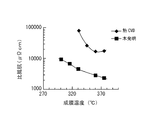
図4は、上記条件で成膜した場合と、触媒体21を加熱せず、従来技術の熱CVD法と同じ条件で成膜した場合のTaXN膜の比抵抗と成膜対象物の温度の関係を示したグラフである。
<Measurement results>
FIG. 4 shows the specific resistance of the Ta x N film and the temperature of the film formation target when the film is formed under the above conditions and when the
本発明方法によれば、成膜対象物の温度が370℃までは比抵抗は温度を上げるほど低下していくことが分かる。 According to the method of the present invention, it can be seen that the specific resistance decreases as the temperature rises until the temperature of the film formation object reaches 370 ° C.
それに対し、従来技術の熱CVD法では、成膜対象物の温度を上げてもTaN膜の比抵抗は20000μΩcm弱までしか下がっていない。 On the other hand, in the conventional thermal CVD method, the specific resistance of the TaN film decreases only to a little less than 20000 μΩcm even when the temperature of the film formation target is increased.
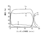
次に、図5、図6は、それぞれ成膜対象物が350℃に昇温されて形成されたTaN膜のAES分析の結果であり、横軸はエッチング時間、即ち膜厚方向の深さであり、縦軸は、構成原子の濃度である。図5は本発明によって成膜した膜の分析結果であり、図6は触媒体を加熱しない従来技術の熱CVD法によって成膜した膜の分析結果である。この結果から本発明のTaN膜は、従来技術のTaN膜よりも炭素成分の含有率が2.4%低いことが分かった。 Next, FIGS. 5 and 6 are the results of AES analysis of the TaN film formed by raising the temperature of the film formation target to 350 ° C., respectively, and the horizontal axis represents the etching time, that is, the depth in the film thickness direction. Yes, the vertical axis represents the concentration of the constituent atoms. FIG. 5 shows the analysis result of the film formed according to the present invention, and FIG. 6 shows the analysis result of the film formed by the conventional thermal CVD method in which the catalyst body is not heated. From this result, it was found that the TaN film of the present invention has a carbon content of 2.4% lower than that of the prior art TaN film.
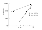
図7は、本発明で作成した02含有率が2.5%のTaN膜と、5.4%のTaN膜に含まれるC成分の原子数比率と、比抵抗の関係を示したものである。この結果によれば、炭素成分が少なくなると比抵抗はが急激に低下することが分かる。 FIG. 7 shows the relationship between the specific resistance and the atomic ratio of the C component contained in the TaN film having a O 2 content of 2.5% and a 5.4% TaN film prepared according to the present invention. is there. According to this result, it can be seen that the specific resistance rapidly decreases as the carbon component decreases.
本発明のTaN膜の方が従来技術の熱CVD法で形成したTaN膜よりも比抵抗が低い理由は、カーボン成分の含有率が低いためと考えられる。 The reason why the specific resistance of the TaN film of the present invention is lower than that of the TaN film formed by the conventional thermal CVD method is considered to be because the content of the carbon component is low.
上記のように、本発明によれば、従来の熱CVD法に比べ、良好な膜質のTaN膜を形成することが出来る。 As described above, according to the present invention, a TaN film having better film quality can be formed as compared with the conventional thermal CVD method.
<実施例2>
しかし、上記図4のグラフからは、2200μΩcmのTaN膜を得るためには成膜対象物を375℃に加熱する必要がある。現在のCu配線工程のプロセス温度の要求は300℃以下であるから、さらに低温化する必要がある。
<Example 2>
However, from the graph of FIG. 4, it is necessary to heat the film formation target to 375 ° C. in order to obtain a 2200 μΩcm TaN film. Since the current process temperature requirement for the Cu wiring process is 300 ° C. or lower, it is necessary to further lower the temperature.
真空チャンバー11を真空排気しながら成膜対象物を真空チャンバー11内に配置し、触媒体21を加熱した後、真空排気と触媒体21の加熱を継続して行いながら、原料ガス(TIMATA)と反応性ガス(NH3ガスやH2ガス)を交互に導入する。
While the
図8は、各ガスの導入のタイミングチャートであり、符号t1は、原料ガスの導入時間、符号t2は原料ガスの導入を停止した後、反応性ガスを導入するまでの排気時間、符号t3は反応性ガスの導入時間、符号t4は、反応性ガスの導入を停止した後、原料ガスを導入するまでの排気時間である。 FIG. 8 is a timing chart of introduction of each gas, where symbol t 1 is the introduction time of the source gas, symbol t 2 is the exhaust time until the introduction of the reactive gas after stopping the introduction of the source gas, symbol t 3 is the introduction time of the reactive gas, and t 4 is the exhaust time until the introduction of the raw material gas after the introduction of the reactive gas is stopped.
原料ガス導入時間t1の間は反応性ガスは導入されず、反応性ガス導入時間t3の間は原料ガスは導入されない。 The raw material gas during the introduction time t 1 is the reactive gas is not introduced during the reaction gas introduction time t 3 is the raw material gas is not introduced.
真空チャンバー11の内部は真空排気系によって継続して真空排気が行われるため、原料ガスの導入と反応性ガスの導入が停止された状態では、真空チャンバー内部の残留ガスは真空排気される。
Since the inside of the
原料ガスの導入時間t1と得られるTaN膜の比抵抗の関係を図9に示す。 FIG. 9 shows the relationship between the introduction time t 1 of the source gas and the specific resistance of the obtained TaN film.
原料ガスの導入時間t1は3〜10秒、原料ガスの導入を停止した後、反応性ガスを導入するまでの時間t2は5秒、反応性ガスの導入時間t3は20秒、反応性ガスの導入を停止した後、原料ガスを導入するまでの時間t4は5秒である。 The source gas introduction time t 1 is 3 to 10 seconds, the time t 2 until the introduction of the reactive gas after stopping the introduction of the source gas is 5 seconds, the reactive gas introduction time t 3 is 20 seconds, the reaction time The time t 4 from when the introduction of the property gas is stopped to when the raw material gas is introduced is 5 seconds.
成膜対象物の温度は、280℃、300℃、320℃の三種類である。他の条件は、実施例1と同じである。
時間t1〜t4を1サイクルとすると、150サイクル繰り返しTaN膜を形成した。
There are three types of temperatures of the film formation target: 280 ° C., 300 ° C., and 320 ° C. Other conditions are the same as those in the first embodiment.
When the time t 1 to t 4 is one cycle, a TaN film was formed repeatedly for 150 cycles.
その結果を、図9に示す。横軸は原料ガス導入時間、縦軸は比抵抗である。原料ガスの導入時間が短いほど、比抵抗が小さいことがわかる。ラジカルと反応するのは、成膜対象物表面に吸着した原料ガスのうち、表面付近にる原子層だけであると考えられるが、1サイクル中の原料ガスの導入時間が短いほど、1サイクル中に表面に吸着する原子層は薄くなるため、ラジカルと反応した低抵抗なTaNの割合が多く、Cの残留量は少なくなる結果、形成されたTaN膜の比抵抗が下がっていくと考えられる。 The result is shown in FIG. The horizontal axis represents the raw material gas introduction time, and the vertical axis represents the specific resistance. It can be seen that the shorter the introduction time of the source gas, the smaller the specific resistance. It is considered that only the atomic layer in the vicinity of the surface of the source gas adsorbed on the surface of the film formation target reacts with the radical, but the shorter the introduction time of the source gas in one cycle, Since the atomic layer adsorbed on the surface becomes thin, the ratio of low resistance TaN reacted with radicals is large and the residual amount of C is reduced. As a result, the specific resistance of the formed TaN film is considered to decrease.
従って、さらに1サイクル中の原料ガスの導入時間を短くすれば、比抵抗は一層低下すると予想される。 Therefore, it is expected that the specific resistance will be further reduced if the introduction time of the source gas in one cycle is further shortened.
<実施例3>
図10は、成膜対象物の温度300℃、原料ガス(TIMATA)の導入時間t1が3秒、排気時間t2、t4が5秒の場合の、反応性ガス(H2ガス)の導入時間t3と形成されたTaN膜の比抵抗の関係を示すグラフである。
<Example 3>
FIG. 10 shows the reactive gas (H 2 gas) when the temperature of the film formation target is 300 ° C., the introduction time t 1 of the source gas (TIMATA) is 3 seconds, and the exhaust times t 2 and t 4 are 5 seconds. is a graph showing the resistivity of the relationship between TaN film formed with the introduction time t 3.
300℃はCu配線プロセスの上限温度であるが、図10の結果から、成膜対象物の加熱温度を300℃にした場合にも、比抵抗2000μΩcmという結果得られた。 Although 300 ° C. is the upper limit temperature of the Cu wiring process, the result of FIG. 10 shows that the specific resistance was 2000 μΩcm even when the heating temperature of the film formation target was 300 ° C.
また、図11はこのTaN膜のAES分析の結果である。膜質を低下させる原因となるカーボン成分の含有率は、従来のCVD法に比べ極めて低く、約1.5%である。この値は図5の場合と比べても低い。 FIG. 11 shows the result of AES analysis of the TaN film. The content of the carbon component that causes the deterioration of the film quality is extremely low as compared with the conventional CVD method, and is about 1.5%. This value is lower than in the case of FIG.
これらのことから、本発明方法は、Cu配線プロセスの要求である
(1)300℃以下の基板温度
(2)炭素成分のない良質な膜
(3)良好なSTEP COVERAGE
を満足させることができる。
From these facts, the method of the present invention is a requirement for the Cu wiring process.
(1) Substrate temperature below 300 ° C
(2) Good quality film without carbon component
(3) Good STEP COVERAGE
Can be satisfied.
なお、上記はTaN膜を形成する場合について説明したが、本発明はTaN膜の形成に限定されるものではなく、真空雰囲気中に原料ガスと反応性ガスを導入し、加熱した触媒体に反応性ガスを接触させて生成されたラジカルが原料ガスを化学反応させ、成膜対象物表面に薄膜が形成されるプロセスに広く用いることができる。 Although the above description has been given of the case where the TaN film is formed, the present invention is not limited to the formation of the TaN film, but the raw material gas and the reactive gas are introduced into the vacuum atmosphere to react with the heated catalyst body. The radicals produced by contacting the reactive gas can be widely used in processes in which a raw material gas is chemically reacted to form a thin film on the surface of the film formation target.
10……真空処理装置
11……真空チャンバー
21……触媒体
40……成膜対象物
10 ……
Claims (10)
前記前処理は前記真空チャンバー内に前記成膜対象物を配置し、前記触媒体を加熱した状態で、前記真空チャンバー内に前記原料ガスを導入せずに前記反応性ガスを導入し、前記触媒体に前記反応性ガスを接触させる薄膜製造方法。 The thin film manufacturing method according to any one of claims 1 to 7, wherein the thin film is formed after performing pretreatment.
In the pretreatment, the film-forming target is placed in the vacuum chamber, the reactive gas is introduced into the vacuum chamber without introducing the source gas, and the catalyst is heated. A method for producing a thin film, wherein the reactive gas is brought into contact with a medium.
Priority Applications (7)
| Application Number | Priority Date | Filing Date | Title |
|---|---|---|---|
| JP2003390391A JP2005158761A (en) | 2003-11-20 | 2003-11-20 | Thin film manufacturing method, semiconductor device and manufacturing method thereof |
| TW093132621A TW200524018A (en) | 2003-11-20 | 2004-10-27 | Method of cleaning surface of semiconductor substrate, method of manufacturing film, method of manufacturing semiconductor device and semiconductor device |
| KR1020040092234A KR101233525B1 (en) | 2003-11-20 | 2004-11-12 | Method of cleaning surface of semiconductor substrate, method of manufacturing film, method of manufacturing semiconductor device and semiconductor device |
| US10/989,541 US20050118810A1 (en) | 2003-11-20 | 2004-11-17 | Method of cleaning surface of semiconductor substrate, method of manufacturing thin film, method of manufacturing semiconductor device, and semiconductor device |
| CN2004100957620A CN1638052B (en) | 2003-11-20 | 2004-11-19 | Method of manufacturing thin film |
| CN200810125094XA CN101330044B (en) | 2003-11-20 | 2004-11-19 | Method of manufacturing thin film |
| US11/710,918 US8216642B2 (en) | 2003-11-20 | 2007-02-27 | Method of manufacturing film |
Applications Claiming Priority (1)
| Application Number | Priority Date | Filing Date | Title |
|---|---|---|---|
| JP2003390391A JP2005158761A (en) | 2003-11-20 | 2003-11-20 | Thin film manufacturing method, semiconductor device and manufacturing method thereof |
Publications (2)
| Publication Number | Publication Date |
|---|---|
| JP2005158761A true JP2005158761A (en) | 2005-06-16 |
| JP2005158761A5 JP2005158761A5 (en) | 2006-11-02 |
Family
ID=34717783
Family Applications (1)
| Application Number | Title | Priority Date | Filing Date |
|---|---|---|---|
| JP2003390391A Pending JP2005158761A (en) | 2003-11-20 | 2003-11-20 | Thin film manufacturing method, semiconductor device and manufacturing method thereof |
Country Status (2)
| Country | Link |
|---|---|
| JP (1) | JP2005158761A (en) |
| CN (1) | CN101330044B (en) |
Cited By (3)
| Publication number | Priority date | Publication date | Assignee | Title |
|---|---|---|---|---|
| WO2007123102A1 (en) * | 2006-04-18 | 2007-11-01 | Ulvac, Inc. | Film forming apparatus and barrier film manufacturing method |
| JP2012184449A (en) * | 2011-03-03 | 2012-09-27 | Taiyo Nippon Sanso Corp | Method for forming metal thin film, metal thin film, and device for forming metal thin film |
| JP7476319B2 (en) | 2020-06-28 | 2024-04-30 | アプライド マテリアルズ インコーポレイテッド | Removal of impurities in doped ALD tantalum nitride |
Families Citing this family (4)
| Publication number | Priority date | Publication date | Assignee | Title |
|---|---|---|---|---|
| US9474163B2 (en) * | 2014-12-30 | 2016-10-18 | Asm Ip Holding B.V. | Germanium oxide pre-clean module and process |
| US10373850B2 (en) | 2015-03-11 | 2019-08-06 | Asm Ip Holding B.V. | Pre-clean chamber and process with substrate tray for changing substrate temperature |
| AT519217B1 (en) | 2016-10-04 | 2018-08-15 | Carboncompetence Gmbh | Apparatus and method for applying a carbon layer |
| US20200306802A1 (en) * | 2017-12-18 | 2020-10-01 | Sekisui Chemical Co., Ltd. | Surface treatment method and surface treatment apparatus |
Family Cites Families (3)
| Publication number | Priority date | Publication date | Assignee | Title |
|---|---|---|---|---|
| JP3436776B2 (en) * | 1993-08-09 | 2003-08-18 | 忠弘 大見 | Wafer cleaning apparatus and cleaning method |
| US6040010A (en) * | 1996-09-10 | 2000-03-21 | Micron Technology, Inc. | Catalytic breakdown of reactant gases in chemical vapor deposition |
| CN1313412A (en) * | 2000-03-10 | 2001-09-19 | 广镓光电股份有限公司 | Process for generating epitaxial layer of III-family nitrode on monocrystal substrate and its products and equipment |
-
2003
- 2003-11-20 JP JP2003390391A patent/JP2005158761A/en active Pending
-
2004
- 2004-11-19 CN CN200810125094XA patent/CN101330044B/en active Active
Cited By (5)
| Publication number | Priority date | Publication date | Assignee | Title |
|---|---|---|---|---|
| WO2007123102A1 (en) * | 2006-04-18 | 2007-11-01 | Ulvac, Inc. | Film forming apparatus and barrier film manufacturing method |
| JPWO2007123102A1 (en) * | 2006-04-18 | 2009-09-03 | 株式会社アルバック | Film forming apparatus and barrier film manufacturing method |
| US8309175B2 (en) | 2006-04-18 | 2012-11-13 | Ulvac, Inc. | Barrier film producing method for a semiconductor |
| JP2012184449A (en) * | 2011-03-03 | 2012-09-27 | Taiyo Nippon Sanso Corp | Method for forming metal thin film, metal thin film, and device for forming metal thin film |
| JP7476319B2 (en) | 2020-06-28 | 2024-04-30 | アプライド マテリアルズ インコーポレイテッド | Removal of impurities in doped ALD tantalum nitride |
Also Published As
| Publication number | Publication date |
|---|---|
| CN101330044B (en) | 2011-01-12 |
| CN101330044A (en) | 2008-12-24 |
Similar Documents
| Publication | Publication Date | Title |
|---|---|---|
| TWI624870B (en) | Procedure for etch rate consistency | |
| US11101174B2 (en) | Gap fill deposition process | |
| US9309598B2 (en) | Oxide and metal removal | |
| US6734102B2 (en) | Plasma treatment for copper oxide reduction | |
| US8183150B2 (en) | Semiconductor device having silicon carbide and conductive pathway interface | |
| JP2017041632A (en) | Selective deposition of materials containing aluminium and nitrogen | |
| JP4914902B2 (en) | Method and apparatus for forming silicide | |
| KR20140014024A (en) | Methods of improving tungsten contact resistance in small critical dimension features | |
| US8895443B2 (en) | N-metal film deposition with initiation layer | |
| KR102394249B1 (en) | Manganese barrier and adhesion layers for cobalt | |
| US8216642B2 (en) | Method of manufacturing film | |
| KR100942684B1 (en) | Method for forming tantalum nitride film | |
| TWI427701B (en) | Film forming device and method for forming barrier film | |
| JP2005158761A (en) | Thin film manufacturing method, semiconductor device and manufacturing method thereof | |
| KR100954715B1 (en) | Method for forming tantalum nitride film | |
| JP4931169B2 (en) | Method for forming tantalum nitride film | |
| TW201445002A (en) | Methods for manganese nitride integration | |
| CN115485819A (en) | Systems and methods for selective metal compound removal | |
| US9269584B2 (en) | N-metal film deposition with initiation layer | |
| US9236467B2 (en) | Atomic layer deposition of hafnium or zirconium alloy films | |
| JP2005166783A (en) | Method for cleaning surface of semiconductor substrate | |
| KR102597990B1 (en) | Method for selective deposition of aluminum and nitrogen containing material | |
| JP2002134436A (en) | Plasma processing apparatus, method thereof and plasma product | |
| JPH05190495A (en) | Manufacture of semiconductor device |
Legal Events
| Date | Code | Title | Description |
|---|---|---|---|
| A521 | Written amendment |
Free format text: JAPANESE INTERMEDIATE CODE: A523 Effective date: 20060914 Free format text: JAPANESE INTERMEDIATE CODE: A821 Effective date: 20060914 |
|
| A621 | Written request for application examination |
Effective date: 20060914 Free format text: JAPANESE INTERMEDIATE CODE: A621 |
|
| A977 | Report on retrieval |
Effective date: 20080104 Free format text: JAPANESE INTERMEDIATE CODE: A971007 |
|
| A131 | Notification of reasons for refusal |
Free format text: JAPANESE INTERMEDIATE CODE: A131 Effective date: 20080708 |
|
| A521 | Written amendment |
Effective date: 20080908 Free format text: JAPANESE INTERMEDIATE CODE: A523 Free format text: JAPANESE INTERMEDIATE CODE: A821 Effective date: 20080908 |
|
| A131 | Notification of reasons for refusal |
Free format text: JAPANESE INTERMEDIATE CODE: A131 Effective date: 20081007 |
|
| A521 | Written amendment |
Free format text: JAPANESE INTERMEDIATE CODE: A821 Effective date: 20081201 |
|
| A02 | Decision of refusal |
Effective date: 20090106 Free format text: JAPANESE INTERMEDIATE CODE: A02 |