JP2005157178A - Image forming method and image forming apparatus - Google Patents
Image forming method and image forming apparatus Download PDFInfo
- Publication number
- JP2005157178A JP2005157178A JP2003398684A JP2003398684A JP2005157178A JP 2005157178 A JP2005157178 A JP 2005157178A JP 2003398684 A JP2003398684 A JP 2003398684A JP 2003398684 A JP2003398684 A JP 2003398684A JP 2005157178 A JP2005157178 A JP 2005157178A
- Authority
- JP
- Japan
- Prior art keywords
- image forming
- photoconductor
- image
- photoreceptor
- forming method
- Prior art date
- Legal status (The legal status is an assumption and is not a legal conclusion. Google has not performed a legal analysis and makes no representation as to the accuracy of the status listed.)
- Pending
Links
Images

Classifications
-
- G—PHYSICS
- G03—PHOTOGRAPHY; CINEMATOGRAPHY; ANALOGOUS TECHNIQUES USING WAVES OTHER THAN OPTICAL WAVES; ELECTROGRAPHY; HOLOGRAPHY
- G03G—ELECTROGRAPHY; ELECTROPHOTOGRAPHY; MAGNETOGRAPHY
- G03G5/00—Recording members for original recording by exposure, e.g. to light, to heat, to electrons; Manufacture thereof; Selection of materials therefor
- G03G5/14—Inert intermediate or cover layers for charge-receiving layers
- G03G5/147—Cover layers
- G03G5/14708—Cover layers comprising organic material
-
- G—PHYSICS
- G03—PHOTOGRAPHY; CINEMATOGRAPHY; ANALOGOUS TECHNIQUES USING WAVES OTHER THAN OPTICAL WAVES; ELECTROGRAPHY; HOLOGRAPHY
- G03G—ELECTROGRAPHY; ELECTROPHOTOGRAPHY; MAGNETOGRAPHY
- G03G15/00—Apparatus for electrographic processes using a charge pattern
- G03G15/50—Machine control of apparatus for electrographic processes using a charge pattern, e.g. regulating differents parts of the machine, multimode copiers, microprocessor control
- G03G15/5033—Machine control of apparatus for electrographic processes using a charge pattern, e.g. regulating differents parts of the machine, multimode copiers, microprocessor control by measuring the photoconductor characteristics, e.g. temperature, or the characteristics of an image on the photoconductor
- G03G15/5045—Detecting the temperature
-
- G—PHYSICS
- G03—PHOTOGRAPHY; CINEMATOGRAPHY; ANALOGOUS TECHNIQUES USING WAVES OTHER THAN OPTICAL WAVES; ELECTROGRAPHY; HOLOGRAPHY
- G03G—ELECTROGRAPHY; ELECTROPHOTOGRAPHY; MAGNETOGRAPHY
- G03G21/00—Arrangements not provided for by groups G03G13/00 - G03G19/00, e.g. cleaning, elimination of residual charge
- G03G21/0005—Arrangements not provided for by groups G03G13/00 - G03G19/00, e.g. cleaning, elimination of residual charge for removing solid developer or debris from the electrographic recording medium
- G03G21/0035—Arrangements not provided for by groups G03G13/00 - G03G19/00, e.g. cleaning, elimination of residual charge for removing solid developer or debris from the electrographic recording medium using a brush; Details of cleaning brushes, e.g. fibre density
-
- G—PHYSICS
- G03—PHOTOGRAPHY; CINEMATOGRAPHY; ANALOGOUS TECHNIQUES USING WAVES OTHER THAN OPTICAL WAVES; ELECTROGRAPHY; HOLOGRAPHY
- G03G—ELECTROGRAPHY; ELECTROPHOTOGRAPHY; MAGNETOGRAPHY
- G03G21/00—Arrangements not provided for by groups G03G13/00 - G03G19/00, e.g. cleaning, elimination of residual charge
- G03G21/0005—Arrangements not provided for by groups G03G13/00 - G03G19/00, e.g. cleaning, elimination of residual charge for removing solid developer or debris from the electrographic recording medium
- G03G21/0058—Arrangements not provided for by groups G03G13/00 - G03G19/00, e.g. cleaning, elimination of residual charge for removing solid developer or debris from the electrographic recording medium using a roller or a polygonal rotating cleaning member; Details thereof, e.g. surface structure
-
- G—PHYSICS
- G03—PHOTOGRAPHY; CINEMATOGRAPHY; ANALOGOUS TECHNIQUES USING WAVES OTHER THAN OPTICAL WAVES; ELECTROGRAPHY; HOLOGRAPHY
- G03G—ELECTROGRAPHY; ELECTROPHOTOGRAPHY; MAGNETOGRAPHY
- G03G5/00—Recording members for original recording by exposure, e.g. to light, to heat, to electrons; Manufacture thereof; Selection of materials therefor
- G03G5/02—Charge-receiving layers
- G03G5/04—Photoconductive layers; Charge-generation layers or charge-transporting layers; Additives therefor; Binders therefor
- G03G5/05—Organic bonding materials; Methods for coating a substrate with a photoconductive layer; Inert supplements for use in photoconductive layers
- G03G5/0528—Macromolecular bonding materials
- G03G5/0557—Macromolecular bonding materials obtained otherwise than by reactions only involving carbon-to-carbon unsatured bonds
- G03G5/0575—Other polycondensates comprising nitrogen atoms with or without oxygen atoms in the main chain
-
- G—PHYSICS
- G03—PHOTOGRAPHY; CINEMATOGRAPHY; ANALOGOUS TECHNIQUES USING WAVES OTHER THAN OPTICAL WAVES; ELECTROGRAPHY; HOLOGRAPHY
- G03G—ELECTROGRAPHY; ELECTROPHOTOGRAPHY; MAGNETOGRAPHY
- G03G5/00—Recording members for original recording by exposure, e.g. to light, to heat, to electrons; Manufacture thereof; Selection of materials therefor
- G03G5/02—Charge-receiving layers
- G03G5/04—Photoconductive layers; Charge-generation layers or charge-transporting layers; Additives therefor; Binders therefor
- G03G5/05—Organic bonding materials; Methods for coating a substrate with a photoconductive layer; Inert supplements for use in photoconductive layers
- G03G5/0528—Macromolecular bonding materials
- G03G5/0589—Macromolecular compounds characterised by specific side-chain substituents or end groups
-
- G—PHYSICS
- G03—PHOTOGRAPHY; CINEMATOGRAPHY; ANALOGOUS TECHNIQUES USING WAVES OTHER THAN OPTICAL WAVES; ELECTROGRAPHY; HOLOGRAPHY
- G03G—ELECTROGRAPHY; ELECTROPHOTOGRAPHY; MAGNETOGRAPHY
- G03G5/00—Recording members for original recording by exposure, e.g. to light, to heat, to electrons; Manufacture thereof; Selection of materials therefor
- G03G5/02—Charge-receiving layers
- G03G5/04—Photoconductive layers; Charge-generation layers or charge-transporting layers; Additives therefor; Binders therefor
- G03G5/05—Organic bonding materials; Methods for coating a substrate with a photoconductive layer; Inert supplements for use in photoconductive layers
- G03G5/0528—Macromolecular bonding materials
- G03G5/0592—Macromolecular compounds characterised by their structure or by their chemical properties, e.g. block polymers, reticulated polymers, molecular weight, acidity
-
- G—PHYSICS
- G03—PHOTOGRAPHY; CINEMATOGRAPHY; ANALOGOUS TECHNIQUES USING WAVES OTHER THAN OPTICAL WAVES; ELECTROGRAPHY; HOLOGRAPHY
- G03G—ELECTROGRAPHY; ELECTROPHOTOGRAPHY; MAGNETOGRAPHY
- G03G5/00—Recording members for original recording by exposure, e.g. to light, to heat, to electrons; Manufacture thereof; Selection of materials therefor
- G03G5/02—Charge-receiving layers
- G03G5/04—Photoconductive layers; Charge-generation layers or charge-transporting layers; Additives therefor; Binders therefor
- G03G5/05—Organic bonding materials; Methods for coating a substrate with a photoconductive layer; Inert supplements for use in photoconductive layers
- G03G5/0528—Macromolecular bonding materials
- G03G5/0596—Macromolecular compounds characterised by their physical properties
-
- G—PHYSICS
- G03—PHOTOGRAPHY; CINEMATOGRAPHY; ANALOGOUS TECHNIQUES USING WAVES OTHER THAN OPTICAL WAVES; ELECTROGRAPHY; HOLOGRAPHY
- G03G—ELECTROGRAPHY; ELECTROPHOTOGRAPHY; MAGNETOGRAPHY
- G03G5/00—Recording members for original recording by exposure, e.g. to light, to heat, to electrons; Manufacture thereof; Selection of materials therefor
- G03G5/02—Charge-receiving layers
- G03G5/04—Photoconductive layers; Charge-generation layers or charge-transporting layers; Additives therefor; Binders therefor
- G03G5/06—Photoconductive layers; Charge-generation layers or charge-transporting layers; Additives therefor; Binders therefor characterised by the photoconductive material being organic
- G03G5/07—Polymeric photoconductive materials
- G03G5/075—Polymeric photoconductive materials obtained otherwise than by reactions only involving carbon-to-carbon unsaturated bonds
- G03G5/076—Polymeric photoconductive materials obtained otherwise than by reactions only involving carbon-to-carbon unsaturated bonds having a photoconductive moiety in the polymer backbone
- G03G5/0763—Polymeric photoconductive materials obtained otherwise than by reactions only involving carbon-to-carbon unsaturated bonds having a photoconductive moiety in the polymer backbone comprising arylamine moiety
- G03G5/0764—Polymeric photoconductive materials obtained otherwise than by reactions only involving carbon-to-carbon unsaturated bonds having a photoconductive moiety in the polymer backbone comprising arylamine moiety triarylamine
-
- G—PHYSICS
- G03—PHOTOGRAPHY; CINEMATOGRAPHY; ANALOGOUS TECHNIQUES USING WAVES OTHER THAN OPTICAL WAVES; ELECTROGRAPHY; HOLOGRAPHY
- G03G—ELECTROGRAPHY; ELECTROPHOTOGRAPHY; MAGNETOGRAPHY
- G03G5/00—Recording members for original recording by exposure, e.g. to light, to heat, to electrons; Manufacture thereof; Selection of materials therefor
- G03G5/14—Inert intermediate or cover layers for charge-receiving layers
- G03G5/147—Cover layers
- G03G5/14708—Cover layers comprising organic material
- G03G5/14713—Macromolecular material
- G03G5/14747—Macromolecular material obtained otherwise than by reactions only involving carbon-to-carbon unsaturated bonds
- G03G5/14769—Other polycondensates comprising nitrogen atoms with or without oxygen atoms in the main chain
-
- G—PHYSICS
- G03—PHOTOGRAPHY; CINEMATOGRAPHY; ANALOGOUS TECHNIQUES USING WAVES OTHER THAN OPTICAL WAVES; ELECTROGRAPHY; HOLOGRAPHY
- G03G—ELECTROGRAPHY; ELECTROPHOTOGRAPHY; MAGNETOGRAPHY
- G03G5/00—Recording members for original recording by exposure, e.g. to light, to heat, to electrons; Manufacture thereof; Selection of materials therefor
- G03G5/14—Inert intermediate or cover layers for charge-receiving layers
- G03G5/147—Cover layers
- G03G5/14708—Cover layers comprising organic material
- G03G5/14713—Macromolecular material
- G03G5/14786—Macromolecular compounds characterised by specific side-chain substituents or end groups
-
- G—PHYSICS
- G03—PHOTOGRAPHY; CINEMATOGRAPHY; ANALOGOUS TECHNIQUES USING WAVES OTHER THAN OPTICAL WAVES; ELECTROGRAPHY; HOLOGRAPHY
- G03G—ELECTROGRAPHY; ELECTROPHOTOGRAPHY; MAGNETOGRAPHY
- G03G5/00—Recording members for original recording by exposure, e.g. to light, to heat, to electrons; Manufacture thereof; Selection of materials therefor
- G03G5/14—Inert intermediate or cover layers for charge-receiving layers
- G03G5/147—Cover layers
- G03G5/14708—Cover layers comprising organic material
- G03G5/14713—Macromolecular material
- G03G5/14791—Macromolecular compounds characterised by their structure, e.g. block polymers, reticulated polymers, or by their chemical properties, e.g. by molecular weight or acidity
-
- G—PHYSICS
- G03—PHOTOGRAPHY; CINEMATOGRAPHY; ANALOGOUS TECHNIQUES USING WAVES OTHER THAN OPTICAL WAVES; ELECTROGRAPHY; HOLOGRAPHY
- G03G—ELECTROGRAPHY; ELECTROPHOTOGRAPHY; MAGNETOGRAPHY
- G03G5/00—Recording members for original recording by exposure, e.g. to light, to heat, to electrons; Manufacture thereof; Selection of materials therefor
- G03G5/14—Inert intermediate or cover layers for charge-receiving layers
- G03G5/147—Cover layers
- G03G5/14708—Cover layers comprising organic material
- G03G5/14713—Macromolecular material
- G03G5/14795—Macromolecular compounds characterised by their physical properties
-
- G—PHYSICS
- G03—PHOTOGRAPHY; CINEMATOGRAPHY; ANALOGOUS TECHNIQUES USING WAVES OTHER THAN OPTICAL WAVES; ELECTROGRAPHY; HOLOGRAPHY
- G03G—ELECTROGRAPHY; ELECTROPHOTOGRAPHY; MAGNETOGRAPHY
- G03G9/00—Developers
- G03G9/08—Developers with toner particles
- G03G9/0819—Developers with toner particles characterised by the dimensions of the particles
-
- G—PHYSICS
- G03—PHOTOGRAPHY; CINEMATOGRAPHY; ANALOGOUS TECHNIQUES USING WAVES OTHER THAN OPTICAL WAVES; ELECTROGRAPHY; HOLOGRAPHY
- G03G—ELECTROGRAPHY; ELECTROPHOTOGRAPHY; MAGNETOGRAPHY
- G03G9/00—Developers
- G03G9/08—Developers with toner particles
- G03G9/0821—Developers with toner particles characterised by physical parameters
-
- G—PHYSICS
- G03—PHOTOGRAPHY; CINEMATOGRAPHY; ANALOGOUS TECHNIQUES USING WAVES OTHER THAN OPTICAL WAVES; ELECTROGRAPHY; HOLOGRAPHY
- G03G—ELECTROGRAPHY; ELECTROPHOTOGRAPHY; MAGNETOGRAPHY
- G03G2215/00—Apparatus for electrophotographic processes
- G03G2215/00025—Machine control, e.g. regulating different parts of the machine
- G03G2215/00071—Machine control, e.g. regulating different parts of the machine by measuring the photoconductor or its environmental characteristics
- G03G2215/00084—Machine control, e.g. regulating different parts of the machine by measuring the photoconductor or its environmental characteristics the characteristic being the temperature
-
- G—PHYSICS
- G03—PHOTOGRAPHY; CINEMATOGRAPHY; ANALOGOUS TECHNIQUES USING WAVES OTHER THAN OPTICAL WAVES; ELECTROGRAPHY; HOLOGRAPHY
- G03G—ELECTROGRAPHY; ELECTROPHOTOGRAPHY; MAGNETOGRAPHY
- G03G2221/00—Processes not provided for by group G03G2215/00, e.g. cleaning or residual charge elimination
- G03G2221/0026—Cleaning of foreign matter, e.g. paper powder, from imaging member
Abstract
Description
本発明は、電子写真方式の画像形成方法及び画像形成装置に関し、具体的には、電子写真感光体をクリーニングする工程を有する画像形成方法及び電子写真感光体をクリーニングする手段を有する画像形成装置に関する。 The present invention relates to an electrophotographic image forming method and an image forming apparatus, and more specifically, to an image forming method having a step of cleaning an electrophotographic photosensitive member and an image forming apparatus having means for cleaning the electrophotographic photosensitive member. .
〔電子写真装置の背景〕
近年、電子写真式の画像形成装置の電子写真用感光体(以下、単に感光体と称する)は有機光導電物質を有する、有機感光体(以下、OPCと称する)が広範囲に利用されている。OPCは各種露光波長に対応した材料を開発し易いことや、製造コストが安いことなどの利点があるが、機械的強度が弱く、多量のプリント時に感光体表面が劣化し易く、また、傷が付き易いなどの問題が発生する場合があった。
[Background of electrophotographic equipment]
In recent years, an electrophotographic photoreceptor (hereinafter simply referred to as a photoreceptor) of an electrophotographic image forming apparatus has been widely used as an organic photoreceptor (hereinafter referred to as OPC) having an organic photoconductive material. OPC has advantages such as easy development of materials corresponding to various exposure wavelengths and low manufacturing costs, but mechanical strength is weak, the surface of the photoreceptor is liable to deteriorate when printing a large amount, and scratches are also present. There were cases where problems such as easy attachment occurred.
特に最近では、市場のニーズとして、カラー化、高画質化に加え、高寿命、メンテナンスフリーといった特性が重視される。 Recently, in particular, market needs have focused on characteristics such as long life and maintenance-freeness in addition to colorization and high image quality.
具体的には、潜像、及び顕像特性の安定性や、耐損耗性等の特性が重要視され、感光体をはじめとしてシステムの化学的劣化、機械的劣化及び電気的劣化などに対する耐久性が、より重要視されるようになってきている。 Specifically, the stability of latent image and visible image characteristics, wear resistance, and other characteristics are regarded as important, and durability against chemical degradation, mechanical degradation, electrical degradation, etc. of systems including photoreceptors. However, it is becoming more important.
一般に使用されているカールソン法の電子写真画像形成装置においては、感光体は帯電、露光、現像、転写、クリーニング工程に繰り返し供されることにより、電気的、機械的な外力により、感光体の損耗や異物の付着が生じる可能性が強い。 In a commonly used Carlson electrophotographic image forming apparatus, the photoconductor is repeatedly subjected to charging, exposure, development, transfer, and cleaning processes, so that the photoconductor is worn away by an electrical or mechanical external force. There is a strong possibility of adhesion of foreign matter.
このような背景から、電子写真感光体には、帯電時のオゾン及び窒素酸化物による化学的劣化、帯電時の放電やクリーニング部材の摺擦による機械的劣化及び電気的劣化などの、化学的・電気的・機械的外力に対する耐久性が求められている。 From such a background, the electrophotographic photosensitive member has chemical and electrical degradation such as chemical degradation due to ozone and nitrogen oxides during charging, mechanical degradation due to discharge during charging and rubbing of the cleaning member, and electrical degradation. Durability against electrical and mechanical external forces is required.
前記の如く要求される様々な特性を満たすため、様々な検討がなされてきた。 Various studies have been made to satisfy the various characteristics required as described above.
例えば、上記のOPCの耐久性を向上させるために、該OPCの耐放電安定性、機械的劣化や、電気的劣化に対する耐久性を向上させる技術が検討されてきた。 For example, in order to improve the durability of the above OPC, techniques for improving the discharge resistance stability, mechanical deterioration, and durability against electrical deterioration of the OPC have been studied.
そのアプローチとして、上記のOPCに対して、硬化性の樹脂を電荷輸送層用の樹脂として用いる方法が報告されている(例えば特許文献1参照)。 As such an approach, a method using a curable resin as a resin for a charge transport layer with respect to the OPC has been reported (see, for example, Patent Document 1).
また、電荷輸送物質を含有する硬化性樹脂を用い、さらに潤滑剤や、酸化防止機能を具備した表面保護層を有するOPCが報告されている(例えば、特許文献2〜6参照)。 In addition, OPC using a curable resin containing a charge transport material and further having a lubricant and a surface protective layer having an antioxidant function has been reported (for example, see Patent Documents 2 to 6).
しかし、OPCの機械的強度が増加し、摩耗速度が低減すると、従来摩耗により有効に除去されていた、感光体表面に付着したトナーや紙粉等に起因する付着物が取れ難くなり、その結果堆積した付着物により、高湿環境下での画像流れ等といった画像品質の低下が発生する場合があった。 However, if the mechanical strength of the OPC increases and the wear rate decreases, it becomes difficult to remove deposits caused by toner or paper dust attached to the surface of the photoreceptor, which have been effectively removed by conventional wear. In some cases, the deposited deposits may cause deterioration in image quality such as image flow in a high humidity environment.
この場合の改善手段として、架橋構造を有する樹脂からなる最表面を有する感光体と、クリーニングブレードからなるクリーニング手段とを配した系で、さらにブラシローラーを有し、繊維の太さ、ブラシ密度といった、該ブラシローラーの形状特性と、該ブラシローラーが感光体に押し当る時の押し圧力や、駆動トルクといった、感光体への設置条件を規定した方法(例えば、特許文献7参照)や、繊維の太さ、ブラシ密度といった、該ブラシローラーの形状特性とブラシのヤング率、感光体に対する設置条件、駆動条件からなる式の範囲を規定した方法(例えば、特許文献8参照)が報告されている。 As an improvement means in this case, a system in which a photoreceptor having the outermost surface made of a resin having a crosslinked structure and a cleaning means made of a cleaning blade are arranged, and further has a brush roller, and the fiber thickness, brush density, etc. , A method (for example, refer to Patent Document 7) that defines the installation characteristics of the brush roller, such as the shape characteristics of the brush roller, the pressing force when the brush roller is pressed against the photosensitive member, and the driving torque. A method (for example, see Patent Document 8) has been reported that defines the range of formulas including the shape characteristics of the brush roller, the Young's modulus of the brush, the installation conditions for the photoreceptor, and the driving conditions such as thickness and brush density.
しかしながら、特許文献7には、画像流れ等の画像結果に関して何ら開示されていない。また、特許文献8には、0.45μm/200kc(1kc=1000コピー)未満の摩耗速度では、感光体劣化の防止に不十分である旨が記載されている。 However, Patent Document 7 does not disclose any image results such as image flow. Further, Patent Document 8 describes that a wear rate of less than 0.45 μm / 200 kc (1 kc = 1000 copies) is insufficient to prevent photoreceptor deterioration.
また、上記の方法において、いわゆる通常の画像流れを抑制できる条件、かつ当然ながらクリーニング性が良好な条件においても、耐刷によりスジ状の画像欠陥が発生する場合があった。このようなスジ状欠陥はハイライト側のハーフトーンで見え易い。特にこのような画像を出力するカラー画像形成装置において課題であり、高画質志向の装置であればより大きな課題である。 In the above method, streak-like image defects may occur due to printing durability even under conditions that can suppress so-called normal image flow and, of course, good cleaning properties. Such streak-like defects are easy to see in the highlight halftone. This is particularly a problem in a color image forming apparatus that outputs such an image, and a larger problem if it is a high-quality-oriented apparatus.
耐刷により発生するスジ状の画像欠陥について、本発明者らが耐磨耗性の異なる種々の感光体について比較評価した結果、摩耗速度が小さい、即ち耐磨耗性が高い感光体で発生し易い傾向が見出された。
本発明は、上記の従来技術の課題を鑑みなされたもので、その目的とするところは、長期に渡って良好な画像を出力することが可能な画像形成方法及び画像形成装置を提供することにある。 The present invention has been made in view of the above-described problems of the prior art, and an object thereof is to provide an image forming method and an image forming apparatus capable of outputting a good image over a long period of time. is there.
また、本発明の他の目的は、長期に渡って良好なクリーニング性を保持し、画像不良が無く、かつ感光体やクリーニング部材の耐久性を向上させる画像形成方法及び画像形成装置を提供することにある。 Another object of the present invention is to provide an image forming method and an image forming apparatus that maintain good cleaning properties for a long period of time, have no image defects, and improve the durability of the photoreceptor and the cleaning member. It is in.
また、本発明の他の目的は、耐刷によるスジ状欠陥等の画像欠陥を防止し、一方では感光体やクリーニング手段の耐久性を高水準で維持することが可能な画像形成方法及び画像形成装置を提供することにある。 Another object of the present invention is to provide an image forming method and an image forming method capable of preventing image defects such as streak-like defects due to printing durability, while maintaining the durability of the photoreceptor and the cleaning means at a high level. To provide an apparatus.
上記目的を達成するために本発明に係る画像形成方法にあっては感光体を帯電する工程と、帯電された前記感光体に潜像を形成する潜像形成工程と、前記潜像を現像剤により現像する現像工程と、現像された現像剤像を転写材に転写する転写工程と、前記感光体上の残留物を除去するクリーニング工程と、前記感光体の回転方向上流側において前記クリーニング工程を補助する摺擦工程と、前記感光体の表面温度を制御する温度制御工程と、を有する画像形成方法であって、前記感光体は、HU(ユニバーサル硬さ値)が150N/mm2以上220N/mm2以下であり、かつ、弾性変形率が43%以上65%以下であることを特徴とする。 In order to achieve the above object, in the image forming method according to the present invention, a step of charging a photosensitive member, a latent image forming step of forming a latent image on the charged photosensitive member, and a developer of the latent image are developed. A developing process for developing the toner image, a transferring process for transferring the developed developer image to a transfer material, a cleaning process for removing residues on the photoconductor, and the cleaning process on the upstream side in the rotational direction of the photoconductor. An image forming method having an auxiliary rubbing step and a temperature control step for controlling the surface temperature of the photoconductor, wherein the photoconductor has a HU (Universal Hardness Value) of 150 N / mm 2 or more and 220 N / mm. mm 2 or less, and wherein the elastic deformation rate is less than or equal to 65% 43% or more.
あるいは、本発明に係る画像形成装置にあっては、感光体と、前記感光体を帯電する帯電手段と、帯電された前記感光体に潜像を形成する潜像形成手段と、前記潜像を現像剤により現像する現像手段と、現像された現像剤像を転写材に転写する転写手段と、前記感光体上の残留物を除去するクリーニング手段と、前記感光体の回転方向上流側において前記クリーニング手段を補助する摺擦部材と、前記感光体の表面温度を制御する温度制御手段と、を有する画像形成装置であって、前記感光体は、HU(ユニバーサル硬さ値)が150N/mm2以上220N/mm2以下であり、かつ、弾性変形率が43%以上65%以下であることを特徴とする。 Alternatively, in the image forming apparatus according to the present invention, a photosensitive member, a charging unit that charges the photosensitive member, a latent image forming unit that forms a latent image on the charged photosensitive member, and the latent image. Developing means for developing with a developer; transfer means for transferring the developed developer image onto a transfer material; cleaning means for removing residues on the photoconductor; and cleaning on the upstream side in the rotational direction of the photoconductor. An image forming apparatus having a rubbing member for assisting the means and a temperature control means for controlling the surface temperature of the photoconductor, wherein the photoconductor has an HU (Universal Hardness Value) of 150 N / mm 2 or more. It is 220 N / mm 2 or less, and the elastic deformation rate is 43% or more and 65% or less.
ここで、前記ユニバーサル硬さ置及び弾性変形率は、温度25℃/湿度50%の環境下でビッカース四角錐ダイヤモンド圧子を用い、最大荷重6mNで押し込み硬度試験により算出した値である。 Here, the universal hardness setting and the elastic deformation rate are values calculated by an indentation hardness test using a Vickers square pyramid diamond indenter under an environment of a temperature of 25 ° C./humidity of 50% and a maximum load of 6 mN.
また、前記感光体の表面温度は、該感光体を使用する装置がおかれた環境の温度よりも、少なくとも3[deg]以上高温となるように制御されることが好適である。 The surface temperature of the photoreceptor is preferably controlled to be at least 3 [deg] higher than the temperature of the environment in which the apparatus using the photoreceptor is placed.
また、前記感光体は、導電性支持体上に感光層及び表面層を有し、該表面層は、少なくとも硬化性樹脂及び電荷輸送性化合物を含有し、前記電荷輸送性化合物は、少なくとも熱、光、放射線のいずれかにより重合、硬化されたものであることが好適である。 The photoreceptor has a photosensitive layer and a surface layer on a conductive support, and the surface layer contains at least a curable resin and a charge transporting compound, and the charge transporting compound contains at least heat, It is preferable that the material is polymerized and cured by either light or radiation.
また、前記電荷輸送性化合物は、同一分子内に1つ以上の連鎖重合性官能基を有するものであることが好適である。 The charge transporting compound preferably has one or more chain polymerizable functional groups in the same molecule.
また、前記感光体の表面温度が少なくとも画像形成開始までに35〜50℃の所定の温度に制御されることが好適である。 Further, it is preferable that the surface temperature of the photoconductor is controlled to a predetermined temperature of 35 to 50 ° C. at least before the start of image formation.
また、前記摺擦工程は、感光体に対して、−150〜+150%の相対速度で摺擦部材を駆動することが好適である。 In the rubbing step, it is preferable that the rubbing member is driven at a relative speed of −150 to + 150% with respect to the photoreceptor.
また、前記摺擦部材は、AskerC硬度で5〜30°の弾性部材、あるいは、0.56〜3.33tex(5D〜30D)のファーブラシからなることが好適である。 The rubbing member is preferably made of an elastic member having an Asker C hardness of 5 to 30 ° or a fur brush of 0.56 to 3.33 tex (5D to 30D).
また、前記感光体の面速度をS[mm/sec]、前記摺擦部材と前記感光体表面の当接部における速度差をΔS[mm/sec]、前記感光体の表面温度をTd[K]、前記摺擦部材が前記感光体に当接する時の該感光体の長手方向単位長さあたりの当接圧をPs[gf/cm]、とした時に、下式で表される範囲であることが好適である。 Further, the surface speed of the photoconductor is S [mm / sec], the speed difference at the contact portion between the rubbing member and the surface of the photoconductor is ΔS [mm / sec], and the surface temperature of the photoconductor is Td [K. ], When the contact pressure per unit length in the longitudinal direction of the photoconductor when the rubbing member is in contact with the photoconductor is Ps [gf / cm], the range is expressed by the following equation. Is preferred.
1E0≦ΔS×Ps×Td/S^2≦5E2
また、前記感光体の面速度をS[mm/sec]、前記摺擦部材と前記感光体表面の当接部における速度差をΔS[mm/sec]、前記ファーブラシのファーの太さをDf[tex]、前記感光体の表面温度をTd[K]、とした時に、下式で表される範囲であることが好適である。
1E0 ≦ ΔS × Ps × Td / S ^ 2 ≦ 5E2
Further, the surface speed of the photoreceptor is S [mm / sec], the speed difference between the rubbing member and the surface of the photoreceptor is ΔS [mm / sec], and the fur thickness of the fur brush is Df. [Tex], where the surface temperature of the photoconductor is Td [K], is preferably in the range represented by the following formula.
1E―1≦ΔS×Df^2×Td/S^2≦1E2
また、前記感光体の面速度S[mm/sec]が100〜350[mm/sec]であることが好適である。
1E-1 ≦ ΔS × Df ^ 2 × Td / S ^ 2 ≦ 1E2
The surface speed S [mm / sec] of the photoconductor is preferably 100 to 350 [mm / sec].
また、前記摺擦部材が前記感光体に対して非平行であることが好適である。 Further, it is preferable that the rubbing member is non-parallel to the photoconductor.
また、前記表面層の厚さが、2μm〜10μmであることが好適である。 The thickness of the surface layer is preferably 2 μm to 10 μm.
また、前記クリーニング工程で用いられるクリーニング部材は、レシプロ及び/又は振動することが好適である。 The cleaning member used in the cleaning step is preferably reciprocating and / or vibrating.
また、前記現像剤に含まれるトナー粒子の平均粒径が3μm〜9μmであることが好適である。 In addition, it is preferable that the average particle size of the toner particles contained in the developer is 3 μm to 9 μm.
また、前記現像剤に含まれるトナー粒子のDSC測定によるガラス転移点Tgが40〜90℃であることが好適である。 Moreover, it is preferable that the glass transition point Tg by DSC measurement of the toner particles contained in the developer is 40 to 90 ° C.
以上説明したように、本発明によれば、長期に渡って良好な画像を出力することが可能な画像形成方法及び画像形成装置を提供することができる。 As described above, according to the present invention, it is possible to provide an image forming method and an image forming apparatus capable of outputting a good image over a long period of time.
また、長期に渡って良好なクリーニング性を保持し、画像不良がなく、かつ感光体やクリーニング部材の耐久性を向上させることができる。 Further, good cleaning properties can be maintained for a long period of time, no image defects can be caused, and the durability of the photosensitive member and the cleaning member can be improved.
また、耐刷によるスジ状欠陥等の画像欠陥を防止し、一方では感光体やクリーニング手段の耐久性を高水準で維持することが可能となる。 In addition, image defects such as streak-like defects due to printing durability can be prevented, and on the other hand, the durability of the photoreceptor and the cleaning means can be maintained at a high level.
以下に図面を参照して、この発明の好適な実施の形態を例示的に詳しく説明する。但し、この実施の形態に記載されている構成部品の寸法、材質、形状、その相対配置などは、特に特定的な記載がない限りは、この発明の範囲をそれらのみに限定する趣旨のものではない。また、以下の説明で一度説明した部材についての材質、形状などは、特に改めて記載しない限り初めの説明と同様のものである。 Exemplary embodiments of the present invention will be described in detail below with reference to the drawings. However, the dimensions, materials, shapes, relative arrangements, and the like of the components described in this embodiment are not intended to limit the scope of the present invention only to those unless otherwise specified. Absent. Further, the materials, shapes, etc. of the members once described in the following description are the same as those in the first description unless otherwise described.
(実施の形態)
図1〜図7を参照して、実施の形態に係る画像形成方法及び画像形成装置について説明する。
(Embodiment)
An image forming method and an image forming apparatus according to an embodiment will be described with reference to FIGS.
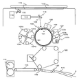
[画像形成装置本体の概略]
はじめに、図1を参照して本実施の形態に係る画像形成装置について説明する。図1は、本実施の形態に係る画像形成装置の模式的断面図である。
[Outline of Image Forming Apparatus Main Body]
First, the image forming apparatus according to the present embodiment will be described with reference to FIG. FIG. 1 is a schematic cross-sectional view of the image forming apparatus according to the present embodiment.
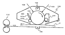
感光体101は、紙面に垂直な軸の周りに回転可能なように支持されており、内部に感光体温度制御手段としてのドラムヒーターDHを有する。感光体101の周囲には、帯電手段102、露光手段103、現像手段104、転写手段122、クリーニング手段107、除電手段108、内部電位センサ109等がそれぞれ適宜な角度位置に設けられている。
The
露光手段103は、画像信号源117と画像信号源117から出射されたレーザ等の光を反射するミラー118とから構成される。
The
画像信号は、原稿台114上に載置された原稿113を、画像読み取り光源115から発せられた光が原稿の濃淡に応じて反射した光をスキャナ116で読み取り、変換したものである。
The image signal is obtained by scanning the original 113 placed on the
感光体101は帯電手段102により一様に帯電され、露光手段103により画像信号に応じた潜像が形成される。前記潜像は、現像手段104(本実施の形態ではカラー画像形成装置のため、イエロー、マゼンタ、シアン、ブラックの四つの現像器104a〜104dを有する)により、現像剤像として現像される。
The
前記現像剤像は、一次転写手段122に一色ごとに転写され、四色分重ね合わされた後、二次転写手段106により、給紙経路119を搬送され、レジストロ一ラ120により搬送タイミングを同期した転写材Pに一括転写される。
The developer image is transferred to the primary transfer unit 122 for each color and is superimposed for four colors, and then conveyed through the
その後、転写材Pは搬送ベルト110により定着手段112に搬送され、現像剤像が転写材P上に定着される。
Thereafter, the transfer material P is transported to the fixing
クリーニング手段107は、クリーニング部材107aとしての弾性ブレードと、感光体101に当接し回転可能な摺擦部材107bと、を有している。必要に応じて、廃トナー搬送手段107c、スクレーパー107d等を具備しても良い。
The
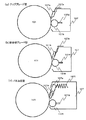
クリーニング部材107aは、周知のクリーニング部材が使用できる。またその固定方法も周知の方法が使用でき、図2に示すように、支持手段である支持板107eの先端に弾性ブレードが固定された、いわゆるチップブレード型や、板状の弾性ブレードが支持板107eに固定された、いわゆる板金板ブレード型や、弾性ブレードを固定した支持板107eがバネ107f等により感光体に当接させられる、いわゆるバネ加圧型などを用いることができる。
A known cleaning member can be used as the cleaning
以下、本実施の形態に係る各要素ごとに説明する。 Hereinafter, each element according to the present embodiment will be described.
[有機光導電体(OPC)]
<層構成>
図3は、本発明の実施の形態に係る電子写真方式の画像形成装置に好適に用いられる感光体の層構成を模式的に示した構成図である。
[Organic photoconductor (OPC)]
<Layer structure>
FIG. 3 is a configuration diagram schematically showing a layer configuration of a photoreceptor preferably used in the electrophotographic image forming apparatus according to the embodiment of the present invention.
本実施の形態に係る感光体300は、導電性支持体301上に感光層302及び表面層(OCL)305が順次積層されたものであり、表面層305の最表面が自由表面306である。
In the
感光層302は、電荷発生物質を含有する電荷発生層303及び電荷輸送物質を含有する電荷輸送層304をこの順に積層した構成を図示しているが、その他にも電荷発生物質と電荷輸送物質を同一層中に分散した単層の感光層302からなる構成をとることも可能である。なお、前者の積層型においては電荷輸送層304が二層以上設けられた構成も可能である。いずれの場合においても、電荷輸送性化合物を感光層302が含有していればよい。
The
但し、電子写真感光体としての特性、特に残留電位などの電気的特性及び耐久性の点より、電荷発生層303/電荷輸送層304/表面層305をこの順に積層した機能分離型の感光体構成で、少なくとも表面層305に、電荷輸送性化合物を含有した連鎖重合性基を有する電荷輸送性化合物の重合体が含有されていることが好ましく、これにより、電荷輸送能を低下させることなく表面層の高耐久化が可能になる。
However, from the viewpoint of characteristics as an electrophotographic photoreceptor, in particular, electrical characteristics such as residual potential and durability, a function-separated photoreceptor structure in which a
また、感光体300は、導電性支持体301と感光層302との間に、導電層や整流性を有する下引き層等からなる導電層307を付加しても良い。導電層307は10〜20μmの範囲で設定するとよい。
In the
<表面層>
本実施の形態に係る感光体としては、高耐久性を確保する観点から、架橋構造を含有する表面層、特に電化輸送機能を有するものが好ましい。
<Surface layer>
As the photoreceptor according to the present embodiment, a surface layer containing a cross-linked structure, particularly one having an electric transport function is preferable from the viewpoint of ensuring high durability.
具体的には、電荷移動層に炭素一炭素二重結合を有するモノマーを含有させ、電荷移動材の炭素一炭素二重結合と熱あるいは光のエネルギーによって反応させて電荷移動層硬化膜を形成した感光体(例えば、特開平5−216249、特開平7−72640号公報等を参照)や、シロキサン系化合物を架橋させ表面層を有する感光体(例えば、特開2002−182536号公報を参照)等が挙げられる。 Specifically, the charge transfer layer contains a monomer having a carbon-carbon double bond, and reacts with the carbon-carbon double bond of the charge transfer material by heat or light energy to form a charge transfer layer cured film. Photoconductors (for example, see JP-A-5-216249 and JP-A-7-72640), photoconductors having a surface layer formed by crosslinking a siloxane compound (for example, see JP-A-2002-182536), etc. Is mentioned.
さらに、摩擦特性を向上させるために、潤滑材としてフッ素原子含有化合物などを含有する表面層であることが好ましく、このような表面層としては、特開2001−166509号公報、特開2001−166517号公報等に記載の熱硬化型表面層、紫外線硬化型表面層、電子線硬化型表面層等がよい。 Furthermore, in order to improve the friction characteristics, a surface layer containing a fluorine atom-containing compound or the like as a lubricant is preferable. Examples of such a surface layer include Japanese Patent Laid-Open Nos. 2001-166509 and 2001-166517. A thermosetting surface layer, an ultraviolet curable surface layer, an electron beam curable surface layer, and the like described in Japanese Laid-Open Patent Publications, etc. are preferable.
[感光体の製造方法]
次に本実施の形態に係る電子写真感光体の製造方法を具体的に示す。
[Method for producing photoreceptor]
Next, a method for manufacturing the electrophotographic photosensitive member according to this embodiment will be specifically described.
表面層より下(支持体側)の層は、周知の感光体を使用することができる。簡略に説明する。 A well-known photoreceptor can be used for the layer below the surface layer (support side). Briefly described.
感光体の支持体としては導電性を有するものであればよい。また、膜の密着性や、レーザなどの可干渉光の干渉防止などにより、該支持体の表面形状を制御することも好ましい。 As the support for the photoreceptor, any material having conductivity can be used. It is also preferable to control the surface shape of the support by adhesion of the film and prevention of interference of coherent light such as a laser.
導電性支持体の上にはバリアー機能と接着機能を持つ下引き層を設けることができる。 An undercoat layer having a barrier function and an adhesive function can be provided on the conductive support.
下引き層は、感光層の接着性改良、塗工性改良、支持体の保護、支持体上の欠陥の被覆、支持体からの電荷注入性改良、また、感光層の電気的破壊に対する保護などのために形成される。下引き層の膜厚としては0.1〜2μmが好ましい。 The undercoat layer improves the adhesion of the photosensitive layer, improves the coatability, protects the support, covers defects on the support, improves the charge injection from the support, and protects the photosensitive layer from electrical breakdown. Formed for. The thickness of the undercoat layer is preferably from 0.1 to 2 μm.
本実施の形態に係る感光体が機能分離型の感光体である場合には、電荷発生層及び電荷輸送層を積層する。電荷発生層に用いる電荷発生物質は周知の材料を使用することができ、その膜厚は5μm以下であることが好ましく、特に0.1〜2μmの範囲であることが好ましい。 When the photoreceptor according to the present embodiment is a function separation type photoreceptor, a charge generation layer and a charge transport layer are laminated. A well-known material can be used for the charge generation material used for the charge generation layer, and the film thickness is preferably 5 μm or less, and particularly preferably in the range of 0.1 to 2 μm.
電荷輸送層の材料も、周知の材料を使用することができ、該電荷輸送層の膜厚は、電荷発生層と合せた厚さが5〜50μmとなるように設定されることが好ましく、特に本発明の如く、耐磨耗性に優れた表面層を有する系では、コスト等の観点からさらに薄層化することが好ましい。より好ましくは30μm以下、最適には20μm以下である。 A well-known material can also be used as the material for the charge transport layer, and the thickness of the charge transport layer is preferably set so that the combined thickness with the charge generation layer is 5 to 50 μm. As in the present invention, in a system having a surface layer excellent in wear resistance, it is preferable to further reduce the thickness from the viewpoint of cost and the like. More preferably, it is 30 μm or less, and optimally 20 μm or less.
表面層は、本実施の形態に係る耐磨耗性、耐侯性はもとより、良好な摩擦特性を有し、クリーニング性を良好に維持するための重要な要素の一つである。 The surface layer has an excellent friction characteristic as well as wear resistance and weather resistance according to the present embodiment, and is one of the important factors for maintaining good cleaning properties.
本実施の形態に係る表面層材料の好適な例として、電荷輸送性化合物を含有する連鎖重合性官能基を有する硬化性樹脂が好ましい。また、硬化性樹脂の構造の骨格中に、電荷輸送性化合物が含有していても構わない。この場合、硬化性を阻害するような電荷輸送性物質を意図的に添加する必要がなく、膜特性の制御が容易にできる。 As a suitable example of the surface layer material according to the present embodiment, a curable resin having a chain polymerizable functional group containing a charge transporting compound is preferable. Further, a charge transporting compound may be contained in the skeleton of the structure of the curable resin. In this case, it is not necessary to intentionally add a charge transporting substance that inhibits curability, and the film characteristics can be easily controlled.
前記連鎖重合性官能基を有する電荷輸送性化合物は、まず、電荷輸送性化合物を含有する溶液として前述の感光体上に塗工される。 The charge transporting compound having a chain polymerizable functional group is first coated on the above-described photoreceptor as a solution containing the charge transporting compound.
その際、必要に応じて潤滑剤を添加することが好ましい。潤滑剤は、上述のフッ素含有樹脂を適宜な分散剤を使用して、表面層材料中に分散させるなどの手法で添加することができる。本実施の形態において、該表面層に含有させる潤滑材の割合は、表面層となる層の全重量に対し、1〜50%が好ましく、より好ましくは5〜30%である。潤滑材が50%より多いと表面層となる層の機械的強度が低下しやすく、1%より少ないと表面層となる層の撥水性、滑り性が充分ではなくなることがある。 At that time, it is preferable to add a lubricant as necessary. The lubricant can be added by a technique such as dispersing the above-described fluorine-containing resin in the surface layer material using an appropriate dispersant. In the present embodiment, the ratio of the lubricant contained in the surface layer is preferably 1 to 50%, more preferably 5 to 30%, based on the total weight of the layer to be the surface layer. When the amount of the lubricant is more than 50%, the mechanical strength of the layer serving as the surface layer tends to be lowered, and when it is less than 1%, the water repellency and slipperiness of the layer serving as the surface layer may not be sufficient.
上述の溶液を塗布後、重合反応をさせるのが一般的であるが、前もって該電荷輸送性化合物を含む溶液を反応させて硬化物を得た後に、再度溶剤中に分散又は溶解させて、表面層を形成させてもよい。これらの溶液を塗布する方法は、例えば、周知のコーティング方法が使用できる。例えば、浸漬コーティング法、スプレイコーティング法、カーテンコーティング法及びスピンコーティング法などが知られているが、効率性/生産性の点からは浸漬コーティング法が好ましい。また蒸着、プラズマその他の公知の製膜方法が適宜選択できる。 Generally, after the above-mentioned solution is applied, a polymerization reaction is performed, but after a solution containing the charge transporting compound is reacted in advance to obtain a cured product, the surface is dispersed or dissolved in a solvent again. A layer may be formed. As a method of applying these solutions, for example, a well-known coating method can be used. For example, a dip coating method, a spray coating method, a curtain coating method, a spin coating method, and the like are known, but the dip coating method is preferable from the viewpoint of efficiency / productivity. Also, vapor deposition, plasma and other known film forming methods can be appropriately selected.
本実施の形態に係る連鎖重合性基を有する電荷輸送性化合物は、熱、光、又は放射線により重合させることができる。好ましくは放射線による重合である。 The charge transporting compound having a chain polymerizable group according to this embodiment can be polymerized by heat, light, or radiation. Polymerization by radiation is preferred.
放射線による重合の最大の利点は重合開始剤を必要としない点であり、これにより非常に高密度な架橋を有する表面層の作製が可能となり、良好な電子写真特性が確保される点である。また、短時間でかつ効率的な重合反応であるがゆえに生産性も高く、さらには放射線の透過性のよさから、厚膜時や添加剤などの遮蔽物質が膜中に存在する際の硬化阻害の影響が非常に小さい点も利点として挙げられる。 The greatest advantage of polymerization by radiation is that it does not require a polymerization initiator, which makes it possible to produce a surface layer having a very high density of crosslinks and to ensure good electrophotographic properties. In addition, because it is a short and efficient polymerization reaction, it is highly productive, and because of its high radiation permeability, it inhibits curing when thick films and additives such as additives are present in the film. There is also an advantage that the influence of is very small.
但し、連鎖重合性基の種類や中心骨格の種類によっては重合反応が進行しにくい場合があり、その際には影響のない範囲内での重合開始剤の添加は可能である。この際使用する放射線とは電子線及びγ線である。電子線照射をする場合、加速器としてはスキャニング型、エレクトロカーテン型、ブロードビーム型、パルス型及びラミナー型等いずれの形式も使用することができる。 However, depending on the type of the chain polymerizable group and the type of the central skeleton, the polymerization reaction may not easily proceed, and in this case, the polymerization initiator can be added within a range that does not affect the polymerization reaction. The radiation used at this time is an electron beam and a γ-ray. In the case of electron beam irradiation, any type of accelerator such as a scanning type, an electro curtain type, a broad beam type, a pulse type, and a laminar type can be used.
電子線を照射する場合に、電気特性及び耐久性能を発現させる上で照射条件が非常に重要である。本実施の形態においては、加速電圧は250kV以下が好ましく、最適には150kV以下である。また線量は好ましくは1Mrad〜100Mradの範囲、より好ましくは1.5Mrad〜50Mradの範囲である。加速電圧が上記を超えると、感光体特性に対する電子線照射のダメージが増加する傾向にある。また、線量が上記範囲よりも少ない場合には硬化が不十分となりやすく、線量が多い場合には感光体特性の劣化がおこりやすい。 When irradiating an electron beam, the irradiation conditions are very important for developing electrical characteristics and durability. In the present embodiment, the acceleration voltage is preferably 250 kV or less, and optimally 150 kV or less. The dose is preferably in the range of 1 Mrad to 100 Mrad, more preferably in the range of 1.5 Mrad to 50 Mrad. When the accelerating voltage exceeds the above, the electron beam irradiation damage tends to increase on the photoreceptor characteristics. Further, when the dose is less than the above range, the curing tends to be insufficient, and when the dose is large, the photoreceptor characteristics are likely to be deteriorated.
また、該重合中の感光体温度の調整は、重合硬化度を制御すると共に、摩擦特性を制御する重要な項目である。本実施の形態において、重合中の温度は50〜150℃が好ましい。50℃以下では重合硬化に時間がかかりコストアップする、あるいは重合硬化が不充分な場合がある。一方、150℃を越す高温では下地の電荷輸送層〜下引き層の損傷等による残留電位の上昇などの影響が出る場合がある。より好ましくは130℃以下である。 Further, the adjustment of the temperature of the photosensitive member during the polymerization is an important item for controlling the degree of polymerization and the friction characteristics. In the present embodiment, the temperature during the polymerization is preferably 50 to 150 ° C. If it is 50 ° C. or less, it may take time for polymerization and curing, resulting in an increase in cost, or polymerization and curing may be insufficient. On the other hand, at a high temperature exceeding 150 ° C., there may be an effect such as an increase in residual potential due to damage of the underlying charge transport layer to undercoat layer. More preferably, it is 130 degrees C or less.
表面層まで形成した後、研磨等の上述の手法で表面形状を制御することも好ましい。 After forming the surface layer, it is also preferable to control the surface shape by the above-mentioned method such as polishing.
ところで、表面層は、上述の如く、保護層としての機能を有している。キズや、偏摩耗により電荷輸送層等の下地が表出することを防止するために、厚いほうが好ましい。一方、該表面層は電荷発生層にまで各種露光を透過させる、窓材としての機能も重要である。該表面層の吸収による透過光の損失や、特に潤滑剤としてフッ素含有樹脂を分散した場合などの光散乱等による感度変動や潜像のブロード化を抑止するためには、薄いほうが好ましい。 By the way, the surface layer has a function as a protective layer as described above. In order to prevent the ground such as the charge transport layer from appearing due to scratches or uneven wear, a thicker one is preferable. On the other hand, the surface layer also has an important function as a window material that transmits various exposures to the charge generation layer. In order to suppress loss of transmitted light due to absorption of the surface layer, sensitivity fluctuations due to light scattering, etc., especially when a fluorine-containing resin is dispersed as a lubricant, and broadening of the latent image, it is preferable to be thin.
該表面層の耐磨耗性、硬度、光吸収特性や散乱特性にも依るが、表面層の厚さは0.5〜10μmが好ましい。より好ましくは1〜7μmである。 Although depending on the wear resistance, hardness, light absorption characteristics and scattering characteristics of the surface layer, the thickness of the surface layer is preferably 0.5 to 10 μm. More preferably, it is 1-7 micrometers.
[表面層の物性]
上述の表面層を有する感光体について、本発明者らがさらに検討を進めた結果、感光体の耐磨耗性、さらにクリーニング部材のダメージ等を鑑みると、該感光体は温度25℃湿度50%の環境下でビッカース四角錐ダイヤモンド圧子を用いて硬度試験を行い、最大荷重6mNで押し込んだ時のHU(ユニバーサル硬さ値)が150N/mm2以上220N/mm2以下であり、かつ、弾性変形率(We)が43%以上65%以下である感光体が、該感光体の耐磨耗性、さらにクリーニング部材の欠けや損耗などを好適に抑止して、システムとしての高耐久性を得る上で好ましいことが判明した。以下にその詳細を述べる。
[Physical properties of the surface layer]
As a result of further investigations on the photoreceptor having the surface layer described above, the photoreceptor has a temperature of 25 ° C. and a humidity of 50% in view of the wear resistance of the photoreceptor and damage to the cleaning member. Hardness test using a Vickers square pyramid diamond indenter under the environment of HU (universal hardness value) when pressed at a maximum load of 6 mN is 150 N / mm 2 or more and 220 N / mm 2 or less, and elastic deformation A photoreceptor having a rate (We) of 43% or more and 65% or less suitably prevents the abrasion resistance of the photoreceptor, and further prevents the chipping or wear of the cleaning member, thereby obtaining high durability as a system. It turned out to be preferable. Details are described below.
一般的に膜の硬度は外部応力に対する変形量が小さいほど高く、電子写真感光体も当然の如く鉛筆硬度やビッカース硬度が高いものが機械的劣化に対する耐久性が向上すると考えられている。しかしながら、これらの測定により得られる硬度が高いものが必ずしも耐久性の向上を望めたわけではなく、上記の範囲が良好であることがわかった。 In general, the hardness of the film is higher as the amount of deformation with respect to external stress is smaller, and it is considered that the electrophotographic photosensitive member having higher pencil hardness or Vickers hardness naturally improves durability against mechanical deterioration. However, it has been found that the high hardness obtained by these measurements does not necessarily improve the durability, and the above range is good.
ユニバーサル硬さ値(以下、HUと称す)と弾性変形率を切り離してとらえることはできないが、例えば、HUが220N/mm2を超えるものであるとき、弾性変形率が43%未満であるとクリーニング部材等に紙粉や現像剤等が、感光体の弾性力が不足しているがゆえに、また、弾性変形率が65%より大きいと弾性変形率は高くても弾性変形量は小さくなってしまうがゆえに、結果として局部的に大きな圧力がかかり、感光体の傷が発生し易くなったり、摩耗量が増大してしまう。あるいは、クリーニング部材が欠けたり損耗する場合がある。よって、HUが高いものが必ずしも感光体として最適ではないと考えられる。 Although universal hardness value (hereinafter referred to as HU) and elastic deformation rate cannot be separated, for example, when HU exceeds 220 N / mm 2 , cleaning is performed when the elastic deformation rate is less than 43%. Paper dust, developer, etc. on the members, etc., because the elastic force of the photoreceptor is insufficient, and if the elastic deformation rate is greater than 65%, the elastic deformation amount is small even if the elastic deformation rate is high. Therefore, as a result, a large pressure is applied locally, so that the photoreceptor is easily damaged and the wear amount is increased. Alternatively, the cleaning member may be chipped or worn. Therefore, it is considered that the one with a high HU is not necessarily optimal as the photosensitive member.
また、HUが150N/mm2未満で弾性変形率が65%を超えるものの場合、例え弾性変形率が高くても塑性変形量も大きくなってしまい、クリーニング部材等に挟まれた紙粉や現像剤が擦られることで該感光体が削れたり細かい傷が発生し、耐久寿命が短くなってしまう。 Further, in the case where the HU is less than 150 N / mm 2 and the elastic deformation rate exceeds 65%, even if the elastic deformation rate is high, the amount of plastic deformation increases, and paper dust or developer sandwiched between cleaning members or the like. By rubbing, the photoconductor is scraped and fine scratches are generated, and the durability life is shortened.
HU及び弾性変形率は、通常環境(温度25±2℃、湿度50±10%;以下
N/N環境と称す)下で、圧子に連続的に荷重をかけ、荷重下での押し込み深さを直読し連続的硬さを求められる、微小硬さ測定装置フィッシャースコープH100V(Fischer社製)を用いて測定した。圧子は対面角136°のビッカース四角錐ダイヤモンド圧子を使用した。荷重の条件は最終荷重6mNまで段階的に(各点0.1secの保持時間で273点)測定した。
HU and elastic deformation rate are determined by applying the load continuously to the indenter under the normal environment (temperature 25 ± 2 ° C, humidity 50 ± 10%; hereinafter referred to as N / N environment). Measurement was performed using a microhardness measuring device, Fischerscope H100V (Fischer), which can be directly read to obtain continuous hardness. The indenter used was a Vickers square pyramid diamond indenter with a face angle of 136 °. The load conditions were measured stepwise up to a final load of 6 mN (273 points with a holding time of 0.1 sec for each point).
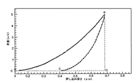
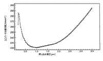
図4は、フィッシャースコープH100V(Fischer社製)を用いて測定した押し込み深さと荷重の関係の一例を示したグラフである。縦軸は荷重(mN)で横軸は押し込み深さh(μm)であり、段階的に荷重を増加させ6mNまで荷重をかけ、その後同様に段階的に荷重を減少させた結果である。 FIG. 4 is a graph showing an example of the relationship between indentation depth and load measured using a Fischer scope H100V (Fischer). The vertical axis represents the load (mN) and the horizontal axis represents the indentation depth h (μm), which is the result of increasing the load stepwise and applying the load to 6 mN, and then decreasing the load stepwise similarly.
HUは、押し込み深さと圧子形状から求められる表面積、及び試験荷重とから算出される。図4に示した押し込み深さvs試験荷重のグラフから、図5に示す、押し込み深さvsHUのグラフが得られる。 HU is calculated from the surface area obtained from the indentation depth and the indenter shape, and the test load. From the graph of indentation depth vs. test load shown in FIG. 4, the graph of indentation depth vs. HU shown in FIG. 5 is obtained.
本発明においては、HUは押し込み深さvs荷重から、6mNで押し込んだ時の同荷重下での押し込み深さから下記式(1)によって規定される。 In the present invention, HU is defined by the following equation (1) from the indentation depth vs. load and the indentation depth under the same load when indented at 6 mN.

硬化性樹脂を用いることで、硬化性樹脂の硬化度を調整することができ、感光体のHUや、特に弾性変形率Weを上述した範囲にすることが容易になるからである。また、電荷輸送物質を含有させたり、電荷輸送性機能を有することで、感度低下、残留電位上昇を抑制させることができるので含有させたほうが好ましい。 This is because by using the curable resin, the degree of cure of the curable resin can be adjusted, and it becomes easy to set the HU of the photosensitive member, particularly the elastic deformation rate We, within the above-described range. In addition, it is preferable to include a charge transporting substance or a charge transporting function because it can suppress a decrease in sensitivity and an increase in residual potential.
[クリーニング装置]
<クリーニング部材(クリーニングブレード)>
クリーニング部材107aのゴム物性は、クリーニングの安定性や、該クリーニング部材の耐久性などの観点から、反発弾性が5〜60%で、硬度が20〜85度の弾性ブレードであることが好ましい。
[Cleaning device]
<Cleaning member (cleaning blade)>
The rubber property of the cleaning
硬度が85度よりも高いと、感光体の局所的な損耗が生じたり、クリーニング性が低下したりする場合がる。一方20度よりも低いと、クリーニング部材107aの捲れが生じ易くなる。反発弾性が5%よりも低いと、感光体表面の凹凸や、異物等により該ブレードが欠けたり、感光体が局所的に損耗したりする場合がある。一方、60%よりも高いとブレードが感光体の移動方向に引き摺られ易くなり、該クリーニング部材107aの捲れや、現像剤の擦り抜けが発生し易くなる場合がある。なお、硬度はJIS−A硬度でJIS K−6253に基づき、また反発弾性はJIS K−6255に基づき測定する。
When the hardness is higher than 85 degrees, local wear of the photosensitive member may occur, or the cleaning property may be deteriorated. On the other hand, if the angle is less than 20 degrees, the cleaning
また、クリーニング部材107aの厚さとしては、1〜4mmが好ましい。1mmよりも薄いと、硬度、反発弾性といった上記のゴム物性を有効に使用できず、クリーニング不良が生じ易くなる。一方、4mmよりも厚いと感光体が局所的に損耗する場合がある。
In addition, the thickness of the cleaning
クリーニング部材107aは、少なくとも感光体と当接する部分に摩擦制御部材を導入したりしても良い。例えば、ナイロンコーティングや、紫外線等による変質加工などを行うと好適である。
For the cleaning
クリーニング部材107aの保持機構は、前述のチップブレード型の場合においては、板金107eが多用され、挟み込み式においては、アルミ、SUSなどの金属製の板金107eと、燐青銅等からなる不図示の背板、さらに該クリーニング部材107aの感光体表面への当接圧を調節するための、バネ107fなどからなる構成が多用される。
As the holding mechanism of the cleaning
クリーニング部材107aにかかる負荷のばらつきを制御する手段としては、保持機構を制御することも有効である。板金の厚さや、形状、固定状態、自由長、感光体への当接圧、当接角等を制御することで、クリーニング部材107aの受けた負荷を好適に分散し、該クリーニング部材107aの摩擦力の偏差を実質的に制御することができる。
Controlling the holding mechanism is also effective as a means for controlling variation in load applied to the cleaning
また、クリーニング部材107aの自由長や、当接角等の調整を併用することも有効である。
It is also effective to use a combination of the adjustment of the free length of the cleaning
クリーニング部材107aの自由長は2〜10mmが、当接角は20〜40°の範囲が、当接圧、及び該当接圧の分布を好適に維持する点で好ましい。
The free length of the cleaning
<摺擦部材>
本実施の形態に係るクリーニング手段は、さらに摺擦部材107bを有している。
<Rubbing member>
The cleaning means according to the present embodiment further has a rubbing
摺擦部材107bは、当接した状態で設置されており、不図示の駆動手段により回転する。そして、摺擦部材107bは、クリーニング部材107aの上流側で回転しながら、感光体101上の帯電生成物を摺擦除去する。
The rubbing
また、摺擦部材107bは、感光体101上の転写残現像剤や、紙粉等の異物を除去するいわゆるクリーニング補助部材として、あるいは、クリーニング部材107aと感光体101の当接部に、外添剤等の潤滑剤を適宜補給する部材としても機能する。
Further, the rubbing
また、摺擦部材107bは、必要に応じてスクレーパー107dを配し、感光体101から除去した異物や、過剰な外添剤を摺擦部材107bから取り除いたりするよう構成すると好適である。
In addition, the rubbing
摺擦部材107bは、感光体101への摺擦力、クリーニング補助部材としてのクリーニング性の能力に加え、感光体101を傷つけないことや、耐久性も重要な要素として挙げられる。そのため、摺擦部材107bとしては、弾性部材からなる弾性ローラーや、繊維からなるファーブラシローラー状の部材が好ましい。
The rubbing
本実施の形態で用いられる弾性ローラーの構成素材は、任意のものを用いることができるが、疎水性で、かつ誘電率が高い高分子重合体を用いるのが好ましい。導電性であると、例えば接地することで現像剤の剥離放電等の抑制にも好ましい。 Any material can be used as the constituent material of the elastic roller used in the present embodiment, but it is preferable to use a high molecular polymer that is hydrophobic and has a high dielectric constant. It is preferable to be conductive, for example, to suppress peeling discharge of the developer by grounding.
弾性ローラーは、芯金上に可澆性部材としてのゴムあるいは発泡体の弾性材を形成することにより作成される。弾性部材はウレタン等の樹脂、硫化剤、発泡剤等により処方され、芯金の上にローラー状に形成後必要に応じて切削、表面研磨して作成することができる。該弾性ローラーは絶縁性、導電性のいずれでもよく、カーボンブラックや金属酸化物等の導電性物質を分散したゴム材や、またこれらを発泡させたり、また、導電性物質を分散せずに、あるいは導電性物質と併用してイオン導電性の材料を用いて低抗調整をすることも可能である。 The elastic roller is formed by forming a rubber or foam elastic material as a flexible member on a cored bar. The elastic member is prescribed by a resin such as urethane, a sulfurizing agent, a foaming agent, and the like, and can be formed by forming a roller shape on a core metal and cutting and polishing the surface as necessary. The elastic roller may be either insulative or conductive, such as a rubber material in which a conductive substance such as carbon black or metal oxide is dispersed, or foaming these, or without dispersing the conductive substance. Alternatively, it is possible to adjust the resistance by using an ion conductive material in combination with a conductive substance.
弾性ローラーの材質としては、弾性発泡体以外にも、弾性体の材料として、エチレン−プロピレン−ジエンポリエチレン(EPDM)、ウレタンゴム、シリコーンゴム等が挙げられる。また、該弾性ローラー表面は、摺擦力や異物除去能力を高めるために、平均セル径が5〜300μmの微小なセル又は凹凸を有していることも好ましい。該セルは単泡、連泡のいずれでも構わない。 Examples of the material of the elastic roller include ethylene-propylene-diene polyethylene (EPDM), urethane rubber, silicone rubber, and the like as the material of the elastic body in addition to the elastic foam. The elastic roller surface preferably has minute cells or irregularities with an average cell diameter of 5 to 300 μm in order to enhance the rubbing force and foreign matter removing ability. The cell may be either single bubble or open cell.
弾性ローラーに用いる弾性部材の硬度はAskre−C硬度で、5度以上30度以下が好ましい。5度未満では、十分な擦過力が無いため表面付着物を除去できない。また、弾性ローラー自体が損耗し、寿命低下が生じる場合がある。一方、30度より大きいと、感光体の表面を傷つけ感光体の寿命を低下させる。 The hardness of the elastic member used for the elastic roller is Askre-C hardness, preferably 5 degrees or more and 30 degrees or less. If it is less than 5 degrees, there is no sufficient rubbing force, so surface deposits cannot be removed. In addition, the elastic roller itself may be worn out and the life may be reduced. On the other hand, if the angle is greater than 30 degrees, the surface of the photoreceptor is damaged and the life of the photoreceptor is reduced.
また、本実施の形態に係るブラシローラーのブラシ構成素材は、任意のものを用いることができるが、疎水性で、かつ誘電率が高い繊維形成性高分子重合体を用いるのが好ましい。 In addition, any material can be used as the brush constituent material of the brush roller according to the present embodiment, but it is preferable to use a fiber-forming high molecular polymer that is hydrophobic and has a high dielectric constant.
このような高分子重合体としては、例えばレーヨン、ナイロン、ポリカーボネート、ポリエステル、メタクリル酸樹脂、アクリル樹脂、ポリ塩化ビニル、ポリ塩化ビニリデン、ポリプロピレン、ポリスチレン、ポリビニルアセテート、スチレン−ブタジエン共重合体、塩化ビニリデン−アクリロニトリル共重合体、塩化ビニル−酢酸ビニル共重合体、塩化ビニル−酢酸ビニル−無水マレイン酸共重合体、シリコーン樹脂、シリコーン−アルキッド樹脂、フェノールホルムアルデヒド樹脂、スチレン−アルキッド樹脂や、ポリビニルアセタール(例えばポリビニルブチラール)等が挙げられる。 Examples of such a high molecular polymer include rayon, nylon, polycarbonate, polyester, methacrylic acid resin, acrylic resin, polyvinyl chloride, polyvinylidene chloride, polypropylene, polystyrene, polyvinyl acetate, styrene-butadiene copolymer, and vinylidene chloride. -Acrylonitrile copolymer, vinyl chloride-vinyl acetate copolymer, vinyl chloride-vinyl acetate-maleic anhydride copolymer, silicone resin, silicone-alkyd resin, phenol formaldehyde resin, styrene-alkyd resin, polyvinyl acetal (for example, Polyvinyl butyral) and the like.
これらのバインダー樹脂は単独であるいは2種以上の混合物として用いることができる。特に、好ましくはレーヨン、ナイロン、ポリエステル、アクリル樹脂、ポリプロピレンである。 These binder resins can be used alone or as a mixture of two or more. Particularly preferred are rayon, nylon, polyester, acrylic resin and polypropylene.
また、前記ブラシは、導電性でも絶縁性でもよく、構成素材にカーボン等の低抵抗物質を含有させ、任意の抵抗に調整したものが使用できる。また、ファーブラシの繊維は直毛状態でも、ループ形状を有していても良い。 The brush may be conductive or insulative, and a constituent material containing a low resistance substance such as carbon and adjusted to an arbitrary resistance can be used. Further, the fiber of the fur brush may be in a straight hair state or may have a loop shape.
ブラシローラーに用いるブラシの単繊維の太さは、0.56tex(5D)以上、3.33tex(30D)以下である。0.56texに満たないと、十分な擦過力が無いため表面付着物を除去できない。また、3.33texより大きいと、繊維が剛直になるため感光体の表面を傷つけ該感光体の寿命を低下させる。 The thickness of the single fiber of the brush used for the brush roller is 0.56 tex (5D) or more and 3.33 tex (30D) or less. If it is less than 0.56 tex, the surface deposits cannot be removed because there is no sufficient rubbing force. On the other hand, if it is larger than 3.33 tex, the fiber becomes stiff so that the surface of the photoreceptor is damaged and the life of the photoreceptor is reduced.
ここで「tex」とは、前記ブラシを構成する繊維の長さ1000mの重量をg(グラム)単位で測定した数値で、従来多用されていた「デニール(D)」に対して、tex=D/9で換算される。 Here, “tex” is a numerical value obtained by measuring the weight of the fiber constituting the brush with a length of 1000 m in units of g (gram), and tex = D with respect to “denier (D)” which has been widely used conventionally. Converted at / 9.
また、前記ブラシの繊維密度は、4×l02f/cm2以上20×103f/cm2以下である。4×l02f/cm2に満たないと、擦過にムラができ付着物を均一に除去することができない。20×103f/cm2より大きいと、ブラシ繊維間に入り込んだ、トナー、異物が除去しきれず、パッキングが発生し前記ブラシの特性が失われる場合がある。 The fiber density of the brush is 4 × 10 2 f / cm 2 or more and 20 × 10 3 f / cm 2 or less. If it is less than 4 × 10 2 f / cm 2 , scratching will be uneven and deposits cannot be removed uniformly. If it is greater than 20 × 10 3 f / cm 2 , the toner and foreign matter that have entered between the brush fibers cannot be completely removed, packing may occur, and the characteristics of the brush may be lost.
これら、弾性ローラー、ファーブラシ等からなる摺擦部材は、アースに接地されていても、また適宜なバイアスが印加されていても良い。 These rubbing members made of an elastic roller, a fur brush, or the like may be grounded or may be applied with an appropriate bias.
[感光体温度制御手段]
<ドラムヒーター>
感光体の温度Tdを制御する好適な方法として、ヒーターが挙げられる。
[Photoconductor temperature control means]
<Drum heater>
A suitable method for controlling the temperature Td of the photoreceptor is a heater.
図1において、感光体101は、その内側に面状のドラムヒーターDHを有している。感光体の内側には、該ドラムヒーターDH以外に、感光体の表面温度Tdを測定するための、不図示の温度測定手段であるサーミスタを有している。
In FIG. 1, the
該温度測定手段と、不図示の制御手段により、該ドラムヒーターDHへの出力が制御され、感光体表面温度Tdが所定の温度に維持される。 The output to the drum heater DH is controlled by the temperature measuring means and a control means (not shown), and the photoreceptor surface temperature Td is maintained at a predetermined temperature.
また、上記の如く感光体内部以外でも、非接触の温度計(不図示)などを設置し、感光体101の表面温度をモニターすることも好ましい。また、ドラムヒーターDHと温度測定手段、制御手段を組み合わせる他にも、所定の温度で抵抗が変動する、自己制御型のヒーターを使用しても良い。
It is also preferable to monitor the surface temperature of the
ドラムヒーターDHは、図1に示す面状ヒーターのみならず、感光体の中心軸を棒状ヒーターにするなど、温度制御手段は周知の方法を使用できる。 As the drum heater DH, not only the planar heater shown in FIG. 1 but also a temperature control means such as a rod-like heater can be used as the temperature control means.
[プロセスカートリッジ]
図6は、本実施の形態に係る画像形成装置に着脱可能なプロセスカートリッジの概略を示す模式的断面図である。図6に示すように、上述の感光体101、一次帯電手段102、現像手段104及びクリーニング手段107などの構成要素のうち、複数のものをプロセスカートリッジ100として一体に結合して構成し、このプロセスカートリッジ100を複写機やレーザービームプリンターなどの電子写真方式の画像形成装置本体に対して着脱可能に構成してもよい。
[Process cartridge]
FIG. 6 is a schematic cross-sectional view showing an outline of a process cartridge that can be attached to and detached from the image forming apparatus according to the present embodiment. As shown in FIG. 6, a plurality of components such as the
例えば、一次帯電手段102、現像手段104及びクリーニング手段107の少なくとも一つを感光体101とともに一体に支持してカートリッジ化して、装置本体のレールなどの案内手段を用いて装置本体に着脱可能なプロセスカートリッジ100とすることができる。帯電手段102は、コロトロン・スコロトロン方式、接触帯電方式など、任意に選択可能である。
For example, a process in which at least one of the
[現像剤]
<現像剤構成>
現像剤は、着色剤や樹脂等からなる母体である分級品、即ちトナー粒子と、該分級品の周囲に外部添加される外添剤を含む。2成分現像剤では、さらにキャリアが含まれる。
[Developer]
<Developer composition>
The developer includes a classified product that is a base made of a colorant, a resin, or the like, that is, toner particles, and an external additive that is externally added around the classified product. The two-component developer further includes a carrier.
現像剤、即ちトナー粒子としては、高解像度(高dpi)に対応する等のために、平均粒径約9μm以下の小粒径が好ましい。また、高画質の観点から、2成分現像材が好ましく利用される。本実施の形態に係る現像剤は、上記に該当する周知の現像剤を使用することができる。 The developer, that is, toner particles, preferably has a small particle diameter of about 9 μm or less in order to cope with high resolution (high dpi). From the viewpoint of high image quality, a two-component developer is preferably used. As the developer according to the present embodiment, a known developer corresponding to the above can be used.
該現像剤のトナーの平均粒径は、重量平均粒径で定義され、該重量平均粒径の好ましい範囲は3〜9μmである。この範囲のトナーを使用することが、画質、及びクリーニングを良好に維持する観点で好ましい。 The average particle size of the toner of the developer is defined by a weight average particle size, and a preferable range of the weight average particle size is 3 to 9 μm. It is preferable to use a toner in this range from the viewpoint of maintaining good image quality and cleaning.
該重量平均粒径が3μm未満のトナーにおいては、トナー全体の表面積が増えることに加え、粉体としての流動性及び攪拌性が低下し、カブリや転写性が悪化傾向となったり、融着以外にも画像の不均一ムラの原因となりやすい他、転写効率の低下から感光体上の転写残トナーが多くなり、クリーニングブレードヘの局所的な衝撃が過剰になり、クリーニング性やトナー融着の抑制が難しくなる。 In the toner having a weight average particle size of less than 3 μm, in addition to the increase in the surface area of the whole toner, the fluidity and agitation as a powder are lowered, and fog and transferability tend to be deteriorated. In addition, it tends to cause unevenness in the image, and the transfer residual toner on the photoconductor increases due to a decrease in transfer efficiency, resulting in excessive local impact on the cleaning blade, thereby suppressing cleaning and toner fusion. Becomes difficult.
また、該重量平均粒径が9μmを超える場合には、文字やライン画像に飛び散りが生じやすく、高解像度が得られにくい。さらに装置が高解像度になっていくと10μm以上のトナーでは1ドットの再現が悪化する傾向にある。 In addition, when the weight average particle diameter exceeds 9 μm, characters and line images are likely to be scattered, and it is difficult to obtain high resolution. Further, as the apparatus becomes higher in resolution, the reproduction of one dot tends to deteriorate with a toner of 10 μm or more.
また、二成分系現像剤で使用される磁性キャリアとしては、磁性体分散型の樹脂キャリアや、表面を樹脂でコートしたフェライト等の磁性体単体の磁性キャリア、磁性体分散型の樹脂キャリア等を使用することができる。 The magnetic carrier used in the two-component developer includes a magnetic material dispersion type resin carrier, a magnetic material such as a ferrite whose surface is coated with a resin, a magnetic material dispersion type resin carrier, etc. Can be used.
また、本発明のトナーは、示差走査型熱量計(DSC)により測定される昇温時のDSC曲線において、ガラス転移点Tgが40〜90℃(好ましくは50〜70℃)の温度領域に少なくとも1つの吸熱ピークを有することが好ましい。Tgが上記範囲よりも低すぎると、高温雰囲気下でトナーが劣化しやすく、また定着時にオフセットが発生しやすくなる。また、Tgが上記範囲よりも高すぎると、定着性が低下する傾向にある。 In addition, the toner of the present invention has at least a glass transition point Tg in a temperature range of 40 to 90 ° C. (preferably 50 to 70 ° C.) in a DSC curve at the time of temperature rise measured by a differential scanning calorimeter (DSC). It preferably has one endothermic peak. If Tg is too lower than the above range, the toner is likely to be deteriorated in a high temperature atmosphere, and offset is liable to occur during fixing. On the other hand, if Tg is too higher than the above range, the fixability tends to decrease.
上記範囲の吸熱ピークを有するトナーを得るためには、示差走査型熱量計(DSC)により測定される昇温時のDSC曲線において40〜90℃に吸熱ピークを有するワックスをトナーに含有させるとよい。 In order to obtain a toner having an endothermic peak in the above range, the toner may contain a wax having an endothermic peak at 40 to 90 ° C. in the DSC curve at the time of temperature rise measured by a differential scanning calorimeter (DSC). .
この範囲内に吸熱ピークを有することにより、トナーの定着性及び対オフセット性を改善できる。トナーの吸熱ピーク温度の測定は示差熱分析測定装置(DSC測定装置)、例えば、DSC−7(パーキンエルマー社製)やDSC2920(TAインスツルメンツジャパン社製)を用い、ASTM規格D3418−82に準じて測定を行う。DSC曲線は、1回昇温、降温させ前履歴を取った後、昇温速度10℃/minで昇温させた時に測定されるDSC曲線を用いる。本実施の形態においては、DSC−7を用い、下記の条件にて測定した。 By having an endothermic peak within this range, it is possible to improve the toner fixing property and offset property. The endothermic peak temperature of the toner is measured using a differential thermal analyzer (DSC measuring device) such as DSC-7 (Perkin Elmer) or DSC2920 (TA Instruments Japan) according to ASTM standard D3418-82. Measure. The DSC curve is a DSC curve that is measured when the temperature is raised at a rate of 10 ° C./min after the temperature is raised and lowered once and the previous history is taken. In this embodiment, DSC-7 was used and measurement was performed under the following conditions.
試料:5〜20mg、好ましくは10mg
測定法:試料をアルミパン中に入れ、リファレンスとして空のアルミパンを用いる。
Sample: 5-20 mg, preferably 10 mg
Measurement method: Place the sample in an aluminum pan, and use an empty aluminum pan as a reference.
温度曲線:昇温I(20℃→180℃、昇温速度10℃/min.)
降温I(180℃→10℃、降温速度10℃/min.)
昇温II(10℃→180℃、昇温速度10℃/min.)
上記測定手順において、昇温IIで測定される吸熱ピークを用い、吸熱ピーク前後の、べ一スラインの中間点の線と、示差熱曲線との交点を本実施の形態におけるガラス転移温度Tgとする。
Temperature curve: Temperature increase I (20 ° C. → 180 ° C., temperature increase rate 10 ° C./min.)
Temperature drop I (180 ° C. → 10 ° C., temperature drop rate 10 ° C./min.)
Temperature increase II (10 ° C. → 180 ° C., temperature increase rate 10 ° C./min.)
In the above measurement procedure, using the endothermic peak measured at the temperature rise II, the intersection of the intermediate line of the base line and the differential heat curve before and after the endothermic peak is defined as the glass transition temperature Tg in the present embodiment. .
以下、実施例により本発明の効果を具体的に説明する。なお、本発明はこれらの実施例に限定されるものではない。 Hereinafter, the effect of the present invention will be specifically described with reference to examples. The present invention is not limited to these examples.
本実施の形態に係る表面層を有する感光体を下記のように作成した。 A photoreceptor having a surface layer according to the present embodiment was prepared as follows.
まず、支持体を含む表面層より下の層に付いては、キヤノン(株)製CP680用の製品ドラムと同処方で、下引き層が2μm、電荷発生層の膜厚が2μm、電荷輸送層の厚さが13μmの感光体を作成した。 First, the layers below the surface layer including the support are of the same formulation as the product drum for CP680 manufactured by Canon Inc., the undercoat layer is 2 μm, the charge generation layer thickness is 2 μm, and the charge transport layer. A photoconductor having a thickness of 13 μm was prepared.
<1.硬化型表面層の製造>
<1−1.放射線硬化型表面層 基本型>
表面層の処方を表1に示す。原料には、下式(M1)の構成の重合性電荷輸送性化合物を使用した。該化合物の生成に際して、適宜シリカゲルカラムを通し精製を行い、不純物の除去を行った。
<1. Production of curable surface layer>
<1-1. Radiation-curable surface layer Basic type>
Table 1 shows the formulation of the surface layer. As a raw material, a polymerizable charge transporting compound having the following formula (M1) was used. In producing the compound, purification was performed through a silica gel column as appropriate to remove impurities.
本実施の形態において感光層に含有させる潤滑材として、テトラフルオロエチレン樹脂粒子(ルブロンL−2、ダイキン工業製;以下、単にテフロン(登録商標)樹脂と称する)26質量部(以下、単に“部”と略称する)、及びモノクロロベンゼン50部を、ガラスビーズを用いたサンドミル装置で分散した。このテトラフルオロエチレン樹脂粒子分散液に上記電荷輸送性化合物(化1)を60部加えて溶解した後、ジクロロメタン30部を加えて表面層用塗料を調製した。 In the present embodiment, as a lubricant contained in the photosensitive layer, 26 parts by mass (hereinafter simply “part”) of tetrafluoroethylene resin particles (Lublon L-2, manufactured by Daikin Industries; hereinafter simply referred to as Teflon (registered trademark) resin). And 50 parts of monochlorobenzene were dispersed in a sand mill apparatus using glass beads. 60 parts of the above charge transporting compound (Chemical Formula 1) was added to and dissolved in this tetrafluoroethylene resin particle dispersion, and then 30 parts of dichloromethane was added to prepare a coating material for the surface layer.
この塗料を前記の感光体上にコーティングし、加速電圧150kV、線量5Mrad、感光体表面温度が110℃の条件で電子線を照射し樹脂を硬化し、膜厚5μmの硬化表面層を形成し、電子写真感光体K0を得た。 This paint is coated on the above photoreceptor, the resin is cured by irradiating with an electron beam under the conditions of an acceleration voltage of 150 kV, a dose of 5 Mrad, and a photoreceptor surface temperature of 110 ° C. to form a cured surface layer having a thickness of 5 μm. An electrophotographic photosensitive member K0 was obtained.
<1−2.テフロン(登録商標)量・電子線量・感光体表面温度条件>
上記、<1−1>で作成した感光体K0に対し、テフロン(登録商標)樹脂含有量、電子線量、製造時の感光体表面温度の条件を振って、感光体K1〜K20を作成した。
<1-2. Teflon (registered trademark) amount, electron dose, photoconductor surface temperature conditions>
Photoconductors K1 to K20 were prepared by changing the Teflon (registered trademark) resin content, the electron dose, and the surface temperature of the photoconductor at the time of production with respect to the photoconductor K0 prepared in <1-1>.
<1−3.電荷輸送性材料>
上記、<1−2>で作成した感光体に対し、さらに下記の電荷輸送性化合物M2、同M3を含有させた感光体K21〜30を作成した。
<1-3. Charge Transport Material>
Photoconductors K21 to 30 containing the following charge transporting compounds M2 and M3 were prepared with respect to the photoconductor prepared in <1-2> above.
(電荷輸送性化合物M2) (Charge transporting compound M2)
カラー用現像剤として、2成分現像剤を下記の要領で作成した。
As a color developer, a two-component developer was prepared in the following manner.
<2−1.キャリア>
本実施例で使用する二成分現像材用のキャリアは、周知のフエライトキャリアなどを使用しても良いし、下記の如き新規なキャリアを用いても良い。
<2-1. Career>
As the carrier for the two-component developer used in this embodiment, a well-known ferrite carrier or the like may be used, or a novel carrier as described below may be used.
本実施例においては、キャリア粒子は、球形重合キャリアで、その製法は、重合法のモノマーにバインダー樹脂と磁性金属酸化物及び非磁性金属酸化物等を添加したモノマー組成物を水系の媒体中で懸濁し、重合させることで球形状のキャリア粒子を得た(なお、生成法は上記手法に限るものではなく、乳化重合法等で生成しても構わず、また他の添加物が入っていても構わない)。 In this example, the carrier particles are spherical polymerized carriers, and the production method is as follows: a monomer composition in which a binder resin, a magnetic metal oxide, a nonmagnetic metal oxide, and the like are added to a polymerization method monomer in an aqueous medium. Suspended and polymerized to obtain spherical carrier particles (Note that the production method is not limited to the above method, it may be produced by an emulsion polymerization method, etc., and other additives are contained. It does not matter.)
<2−1−1.キャリアの製造例>
個数平均粒径O.24μmの強磁性体であるマグネタイト粉(FeO・Fe2O3)と、個数平均粒径0.60μmの非磁性体のα−Fe2O3粉に対し、夫々5.5重量%のシラン系カップリング剤(3−(2−アミノエチルアミノプロピル)ジメトキシシラン)を加え、容器内にて100℃以上で高速混合撹拌して、各金属酸化物微粒子の親油化処理を行った。
<2-1-1. Examples of carrier production>
Number average particle size O.D. A silane system containing 5.5% by weight of magnetite powder (FeO · Fe 2 O 3 ), which is a 24 μm ferromagnetic material, and nonmagnetic α-Fe 2 O 3 powder having a number average particle size of 0.60 μm, respectively. A coupling agent (3- (2-aminoethylaminopropyl) dimethoxysilane) was added, and the mixture was stirred and mixed at a high speed at 100 ° C. or higher in the container to perform lipophilic treatment of each metal oxide fine particle.
次いで、上記の各金属酸化物微粒子を含む下記の組成(C1)を、28重量%NH4OH水溶液を含む水からなる水性媒体の入ったフラスコに入れ、撹拌、混合しながら40分間で85℃まで昇温して、この温度を維持しながら3時間反応、熱硬化させた。続いて、30℃まで冷却し、さらに水を添加した後、上澄み液を除去し、沈殿物を水洗し、風乾した。その後に、減圧下(5mmHg以下)にて50〜60℃で乾燥して、重合法によって磁性樹脂キャリアを得た。 Next, the following composition (C1) containing each of the above metal oxide fine particles was placed in a flask containing an aqueous medium composed of water containing an aqueous 28 wt% NH 4 OH solution and stirred at 85 ° C. for 40 minutes while mixing. The temperature was raised to 1, and the reaction and thermal curing were carried out for 3 hours while maintaining this temperature. Subsequently, after cooling to 30 ° C. and adding water, the supernatant was removed, and the precipitate was washed with water and air-dried. Then, it dried at 50-60 degreeC under pressure reduction (5 mmHg or less), and obtained the magnetic resin carrier by the polymerization method.
組成(C1)
・フェノール・・・10重量部
・ホルムアルデヒド溶液(ホルムアルデヒド40重量%、メタノール10重量%、水5重量0%)・・・6重量部
・親油化処理したマグネタイト粉・・・60重量部
・親油化処理したα−Fe2O3粉・・・40重量部
さらに、上記で得られた磁性樹脂キャリアをコア粒子として、この表面に下記の方法で、熱硬化性のシリコーン樹脂をコートした。
Composition (C1)
-Phenol: 10 parts by weight-Formaldehyde solution (formaldehyde 40% by weight, methanol 10% by weight, water 5% 0%) ... 6 parts by weight-Lipophilicized magnetite powder ... 60 parts by weight Oil-treated α-Fe 2 O 3 powder: 40 parts by weight Further, the magnetic resin carrier obtained above was used as core particles, and the surface was coated with a thermosetting silicone resin by the following method.
磁性キャリア表面のコート樹脂量が1.0重量%となるように、トルエンを溶媒として、10重量%のシリコーン樹脂材料を含むコート溶液を作製した。この溶液に剪断応力を連続して加えながら溶媒を揮発させて、コア粒子表面へのコートを行った。次に、コート溶液がコートされた磁性キャリアを、200℃で1時間キュアし、解砕した後、200メッシュの篩で分級して、表面にシリコーン樹脂がコートされた磁性体分散型の磁性樹脂キャリアCを得た。 A coating solution containing 10% by weight of a silicone resin material was prepared using toluene as a solvent so that the amount of the coating resin on the surface of the magnetic carrier was 1.0% by weight. While the shear stress was continuously applied to this solution, the solvent was volatilized to coat the surface of the core particles. Next, the magnetic carrier coated with the coating solution is cured at 200 ° C. for 1 hour, crushed, classified by a 200-mesh sieve, and a magnetic material dispersion type magnetic resin whose surface is coated with a silicone resin Carrier C was obtained.
上記で得られた磁性樹脂キャリアCについて粒径を測定したところ、ニレコ杜製の画像処理解析装置Luzex3により測定した個数平均粒径は28.3μmであった。また、1キロエルステッドにおける磁化の強さは129emu/cm3であった。磁化の強さは、理研電子(株)製の振動磁場型磁気特性自動記録装置BHV−30を用いて測定した。 When the particle diameter of the magnetic resin carrier C obtained above was measured, the number average particle diameter measured by an image processing analyzer Luzex3 manufactured by Nireko Kashiwa was 28.3 μm. Moreover, the strength of magnetization at 1 kilo Oersted was 129 emu / cm 3 . The strength of magnetization was measured using an oscillating magnetic field type magnetic property automatic recording apparatus BHV-30 manufactured by Riken Denshi Co., Ltd.
<2−2.非磁性トナー>
<2−2−1.非磁性トナーの製造>
高速撹拌装置TK−ホモミキサーを備えた四つ口フラスコに、イオン交換水900重量部とポリビニルアルコール100重量部とを投入し、回転数を1200rpm調整し、60℃に加熱して水系媒体を作製した。一方、下記の組成(T1)を混合し、60℃に加温した後、TK式ホモミキサー(特殊機化工業製)を用いて回転数12000rpmで攪拌した。さらにこれに2,2−アゾビスイソブチロニトリル3重量部を溶解させた重合性単量体組成物を、先に作製した水系媒体中に投入し、60℃で、窒素気流下でTK式ホモミキサーにて10000rpmで10分間撹枠して、その後パドル撹拌翼で撹拌しつつ80℃に昇温し、10時間反応させた。重合反応終了後、減圧下で残存モノマーを除去して、さらに冷却後、塩酸を加えてリン酸カルシウムを溶解させた後、濾過、水洗、乾燥して重合体トナーTを得た。ここでは、黒色トナーの製造例を示す。
<2-2. Non-magnetic toner>
<2-2-1. Production of non-magnetic toner>
A four-necked flask equipped with a high-speed stirring device TK-homomixer is charged with 900 parts by weight of ion-exchanged water and 100 parts by weight of polyvinyl alcohol, adjusted to 1200 rpm, and heated to 60 ° C. to produce an aqueous medium. did. On the other hand, the following composition (T1) was mixed, heated to 60 ° C., and then stirred at a rotational speed of 12000 rpm using a TK homomixer (manufactured by Tokushu Kika Kogyo). Furthermore, the polymerizable monomer composition in which 3 parts by weight of 2,2-azobisisobutyronitrile was dissolved was put into the aqueous medium prepared previously, and the TK type was obtained at 60 ° C. under a nitrogen stream. The mixture was stirred with a homomixer at 10,000 rpm for 10 minutes, and then heated to 80 ° C. while stirring with a paddle stirring blade, and allowed to react for 10 hours. After completion of the polymerization reaction, the residual monomer was removed under reduced pressure, and after cooling, hydrochloric acid was added to dissolve calcium phosphate, followed by filtration, washing with water and drying to obtain a polymer toner T. Here, an example of manufacturing a black toner is shown.
組成(T1)
・スチレン単量体・・・90重量部
・n一ブチルアクリレート単量体・・・22重量部
・カーボンブラック・・・10重量部
・サリチル酸金属化合物・・・1重量部
・離型剤・・・20重量部
続いて、上記の重合体トナーT0.9重量部をメタノール5.0重量部に分散し、その後、ケイ素化合物として、テトラエトキシシラン0.5重量部、メチルトリエトキシシラン0.3重量部を溶解させ、さらに、50重量部のメタノールを添加した。続いて、これに、28重量%NH4OH水溶液10重量部に対し100重量部のメタノールを添加した溶液を滴下しながら加え、室温で48時間攪拌した。
Composition (T1)
Styrene monomer: 90 parts by weight n-Butyl acrylate monomer: 22 parts by weight Carbon black: 10 parts by weight Metal salicylic acid compound: 1 part by weight
反応終了後に、得られた粒子を精製水で洗浄し、次いでメタノールで洗浄した後、粒子を濾別、乾燥し、平均粒径は6.5μm、形状係数SF1が1.06のトナー粒子Tを得た。本トナーはTg=65℃であった。 After completion of the reaction, the obtained particles are washed with purified water and then washed with methanol, and then the particles are filtered and dried to obtain toner particles T having an average particle size of 6.5 μm and a shape factor SF1 of 1.06. Obtained. This toner had Tg = 65 ° C.
<2−2−2.外添剤の製造>
一方、外添剤に使用する無機微粒子として、個数平均一次粒径9nmのシリカにヘキサメチルジシラザンで処理をした後シリコーンオイルで処理し、処理後のBET値が200m2/gの疎水性シリカ微粉体を準備した。
<2-2-2. Manufacture of external additives>
On the other hand, as inorganic fine particles used for external additives, silica having a number average primary particle size of 9 nm is treated with hexamethyldisilazane and then treated with silicone oil, and the treated BET hydrophobic silica having a BET value of 200 m 2 / g. A fine powder was prepared.
その他にも、フッ化ビニリデン微粉末、ポリテトラフルオロエチレン微粉末等のフッ素系樹脂粉末、湿式製法シリカ、乾式製法シリカ等の微粉末シリカ、微粉末酸化チタン、微粉末アルミナ、これらをシランカップリング剤、チタンカップリング剤、シリコーンオイルで表面処理して疎水性を施した処理シリカ、処理酸化チタン、処理アルミナ等を使用することができる。 In addition, fluorine resin powders such as vinylidene fluoride fine powder and polytetrafluoroethylene fine powder, fine powder silica such as wet process silica and dry process silica, fine powder titanium oxide, fine powder alumina, and silane coupling Agents, titanium coupling agents, treated silica surface-treated with silicone oil, treated silica, treated titanium oxide, treated alumina, and the like can be used.
<2−2−3.外添工程>
外添剤として、トナー粒子100質量部に対し、疎水性シリカ微粉体1.0部を加え、三井三池化工機(株)製ヘンシェルミキサーを用い、攪拌羽根の周速を40m/secとして3分間混合し、非磁性トナーTを調製した。
<2-2-3. External process>
As an external additive, 1.0 part of hydrophobic silica fine powder is added to 100 parts by mass of toner particles, and a Henschel mixer manufactured by Mitsui Miike Chemical Co., Ltd. is used, and the peripheral speed of the stirring blade is 40 m / sec for 3 minutes. By mixing, a nonmagnetic toner T was prepared.
<2−3.現像剤>
現像剤として、上記の磁性樹脂キャリアCと、非磁性トナーTを、質量比でT/C=8%になるように混合し、十分に撹拌して現像器用現像剤を作成した。また、該非磁性トナーTを耐久中の補給用現像剤とした。
<2-3. Developer>
As the developer, the magnetic resin carrier C and the nonmagnetic toner T were mixed so that the mass ratio was T / C = 8%, and stirred sufficiently to prepare a developer for the developer. Further, the nonmagnetic toner T was used as a replenishing developer for durability.
<2−4.評価装置>
上記で作製した電子写真感光体、摺擦部材を含むクリーニング手段、及び感光体温度制御手段の評価のために、キヤノン(株)製CP680、同杜製IR6000、同杜製CLC5000を改造して使用した。
<2-4. Evaluation device>
For the evaluation of the electrophotographic photosensitive member produced above, the cleaning means including the rubbing member, and the photosensitive member temperature control means, the Canon CP680, the Doyo IR6000, and the Doyo CLC5000 are modified and used. did.
CP680は、現像手段や転写手段等の位置は製品の状態のままで、現像手段を2成分現像手段にし、カートリッジのクリーニング部材の上流側に、摺擦部材及び該摺擦部材の駆動手段を設置した。感光体の内部に面状ヒーター及びサーミスタを設け、感光体の温度を制御可能とした。また、帯電手段をスコロトロンに変更した。 CP680 is a two-component developing unit with the developing unit, transfer unit and the like being in the product state, and a rubbing member and a driving unit for the rubbing member are installed upstream of the cleaning member of the cartridge. did. A sheet heater and a thermistor are provided inside the photoconductor so that the temperature of the photoconductor can be controlled. Also, the charging means was changed to Scorotron.
また、IR6000も現像手段を2成分現像方式に変更し、さらに図1の如きカラー画像形成装置に変更し、クリーニング手段中のマグネットローラーを別の摺擦部材が取り付けられるようにし、さらに該摺擦部材を駆動自在とした。また、ネガ帯電性の感光体を使用し、反転現像で画像形成できるように、電源の極性変更等を行った。 The IR 6000 also changes the developing unit to a two-component developing system, and further changes to a color image forming apparatus as shown in FIG. 1, so that another rubbing member can be attached to the magnet roller in the cleaning unit, and the rubbing is further performed. The member can be driven freely. Further, the polarity of the power source was changed so that an image can be formed by reversal development using a negatively chargeable photoconductor.
また、CLC5000は、図7に示すように、クリーニング部を上方にずらし、駆動自在の摺擦部材を設置できるようにした。 In addition, as shown in FIG. 7, the CLC 5000 is configured such that the cleaning unit is shifted upward and a freely slidable friction member can be installed.
IR6000,CLC5000については、感光体温度Td制御手段として、IR6000及びCLC5000の製品に既存のヒーターを流用し、該ヒーター制御回路を一部改造して使用した。 For IR6000 and CLC5000, the existing heater was used for the IR6000 and CLC5000 products as the photoreceptor temperature Td control means, and the heater control circuit was partially modified and used.
なお、上記いずれの評価機においても、現像剤は前述のオイルレス非磁性2成分現像剤(外添剤を有する非磁性ワックス内添トナー、磁性キャリアからなる)とし、定着手段を該現像剤に適応するように改造した。また、感光体の面速度を調整できるようにした。当然ながら、紙搬送や現像手段、転写手段等も、該感光体の面速度に同調して速度が調整される。また、クリーニング手段に回収された転写残トナーや紙粉等は、廃トナー搬送手段107c等の搬送手段により不図示の廃トナーボックスに回収されるようにした。さらに電位評価を行えるように露光量や帯電条件の調整や、電位計の設置が可能にする等の改造を施した。なお、電位計はTRek杜製344、555P−1を用い、専用治具にて現像手段位置に設置して電位を測定する。 In any of the above evaluation machines, the developer is the above-mentioned oilless non-magnetic two-component developer (consisting of a non-magnetic wax-added toner having an external additive and a magnetic carrier), and the fixing means is the developer. Modified to adapt. In addition, the surface speed of the photoreceptor can be adjusted. Of course, the speed of paper transport, developing means, transfer means, etc. is adjusted in synchronism with the surface speed of the photoconductor. Further, the transfer residual toner, paper dust, and the like collected by the cleaning unit are collected in a waste toner box (not shown) by a conveyance unit such as a waste toner conveyance unit 107c. Furthermore, modifications such as adjustment of exposure amount and charging conditions and installation of an electrometer were made so that potential evaluation could be performed. The electrometer uses 344, 555P-1 manufactured by TRek, and is installed at the position of the developing means with a dedicated jig to measure the potential.
<3.摺擦部材>
上記の評価機に設置する摺擦部材として、周知の方法で、φ8の芯金上にカーボンを分散した発泡ウレタンからなる弾性ローラーDR1を作成した。該弾性ローラーDR1は、平均孔径がφ100μmの単泡セルを多数有する。Asker−C硬度は20度で、感光体に0.5mm侵入するように設置した。また、クリーニング装置内には、該弾性ローラーに0.2mm侵入するようにスクレーパーを作成、設置した。
<3. Rub member>
As a rubbing member to be installed in the evaluation machine, an elastic roller DR1 made of urethane foam in which carbon is dispersed on a φ8 core metal is prepared by a known method. The elastic roller DR1 has a large number of single bubble cells having an average pore diameter of φ100 μm. Asker-C hardness was 20 degrees, and it was installed so as to penetrate 0.5 mm into the photoreceptor. Further, a scraper was prepared and installed in the cleaning device so as to penetrate 0.2 mm into the elastic roller.
また、カーボンを分散させた、2tex(18D)のレーヨンを、9.3×10³f/cm2(60kf/inch2)で、感光体に1.5mm侵入するようにブラシローラーBR1を作成した。また、クリーニング装置内には、該ブラシローラーに0.5mm侵入するようにスクレーパーを作成し、感光体に並行に当接するように設置した。 In addition, the brush roller BR1 was prepared so that a 2 tex (18D) rayon in which carbon was dispersed was 9.3 × 10 3 f / cm 2 (60 kf / inch 2 ) so as to penetrate 1.5 mm into the photosensitive member. . Further, a scraper was prepared in the cleaning device so as to penetrate 0.5 mm into the brush roller, and installed so as to abut on the photoconductor in parallel.
該弾性ローラー、及び該ブラシローラーの駆動は、感光体の駆動に同調して、任意の面速度で回転するようにした。 The elastic roller and the brush roller were rotated at an arbitrary surface speed in synchronism with the driving of the photosensitive member.
該摺擦部材の駆動条件は、感光体の面速度Sに対する相対速度[%〕で示す。なお、+は感光体に対し順方向、−はカウンター方向であり、例えば+100%は感光体と連れ回る状態、0%は停止状態、−100%は、感光体面速度と同速度でカウンター方向に回転している状態を指す。 The driving condition of the rubbing member is indicated by a relative speed [%] with respect to the surface speed S of the photoreceptor. Note that + is the forward direction with respect to the photoconductor, − is the counter direction, for example, + 100% is the state where the photoconductor is rotated, 0% is the stop state, and −100% is the counter speed at the same speed as the photoconductor surface speed. Refers to the rotating state.
また、該感光体と該摺擦部材の相対速度差の絶対値ΔS[m/sec]は、感光体の面速度Sと相対速度差から算出される。 The absolute value ΔS [m / sec] of the relative speed difference between the photoconductor and the rubbing member is calculated from the surface speed S of the photoconductor and the relative speed difference.
<4.評価(ドラムのユニバーサル硬さ値HU、弾性変形率We)>
上記で作製した電子写真感光体について、初期の電子写真特性、繰り返し使用時の電子写真特性及び画像を評価した。なお、感光体は、ユニバーサル硬さHU弾性変形率We測定用、耐刷試験用に使用するため、同一処方で複数本作成した。
<4. Evaluation (Drum Universal Hardness Value HU, Elastic Deformation Rate We)>
The electrophotographic photoreceptor produced above was evaluated for initial electrophotographic characteristics, electrophotographic characteristics during repeated use, and images. Note that a plurality of photoconductors were prepared with the same prescription for use in universal hardness HU elastic deformation rate We measurement and printing durability test.
初期の電子写真特性及び耐久性は、この感光体を、該感光体の外径に応じて、上述のキヤノン(株)製IR6000改造機(以下、IR6000と称する)、CLC5000改造機(CLC5000と称する)、CP680改造機(CP680と称する)に装着して評価した。なお、感光体の面速度は製品のままとした。 The initial electrophotographic characteristics and durability of the photoconductor are the above-mentioned IR6000 remodeled machine manufactured by Canon Inc. (hereinafter referred to as IR6000) and CLC5000 remodeled machine (referred to as CLC5000) according to the outer diameter of the photoconductor. ), Mounted on a modified CP680 (referred to as CP680) and evaluated. The surface speed of the photoconductor was kept as a product.
クリーニング部材(ブレード、及び該ブレードの支持方法)は製品のままとした。また上記<3>で作成した弾性ローラーDR1、及びスクレーパーを有するクリーニング装置を使用し、感光体に対して感光体の面速度Sに対し、相対速度70%の順方向で回転するようにした。 The cleaning member (blade and supporting method of the blade) was left as a product. In addition, the elastic roller DR1 prepared in the above <3> and a cleaning device having a scraper were used, and the photosensitive member was rotated in the forward direction with a relative speed of 70% with respect to the surface speed S of the photosensitive member.
耐久は、朝メインスイッチをONして、A4サイズの紙を1枚間欠で、4k枚/目で耐久し、夜間はメインスイッチオフとした。また、感光体表面温度Tdは、メインスイッチオン後、評価装置のウォームアップ中に40±2℃まで昇温して、本体電源オン(メインオン)中は、上記の温度範囲で維持されるようにした下で、初期の感光体電気特性評価、硬度物性評価を行った。
初期の感光体電気特性評価として、現像手段を取り外し、電位計を設置して、帯電手段であるスコロトロンのワイヤには−800μAの電流を流し、グリッドには吸込み電源を用い−600Vの電圧が印加されるようにした。この状態で暗部電位Vdを測定した。次に、グリッドヘの印加電圧を調整して暗部電位−600Vに設定し、−150Vに光減衰させるために必要な光量としてVl感度を、及び感度の3倍の光量を照射したときの電位として残留電位Vslを測定した。
For durability, the main switch was turned on in the morning, one piece of A4 size paper was intermittently endured at 4k sheets / eye, and the main switch was turned off at night. The photosensitive member surface temperature Td is raised to 40 ± 2 ° C. during the warm-up of the evaluation apparatus after the main switch is turned on, and is maintained in the above temperature range when the main body power is turned on (main on). Under these conditions, the initial electrical property evaluation and hardness physical property evaluation were performed.
As an initial evaluation of the electrical characteristics of the photoreceptor, the developing means is removed, an electrometer is installed, a current of −800 μA is passed through the scorotron wire as the charging means, and a voltage of −600 V is applied to the grid using a suction power source. It was made to be. In this state, the dark portion potential Vd was measured. Next, the voltage applied to the grid is adjusted to set the dark part potential to -600V, and the Vl sensitivity is used as the amount of light necessary to attenuate the light to -150V, and the potential when the amount of light that is three times the sensitivity is irradiated. The potential Vsl was measured.
電気特性評価には、参考として、CTL(電荷輸送層)がK0〜K30のCTL+表面層と同等の厚さになるように作成し、表面層を作成していない感光体NSL(No Surface Layer)を、同様に評価した。 The electrical characterization, reference as, CTL (charge transporting layer) is prepared so as to have a thickness of equal to CTL + surface layer of K0~K30, to create a surface layer have not photoreceptor NSL (N o S urface L layer) was evaluated in the same manner.
結果、本実施例で作成した感光体K0〜K30は、NSLと同等の帯電特性、感度特性、残電特性を有し、表面層による感度低下や、Vsl増加も無く、良好な電気特性を示した。 As a result, the photoconductors K0 to K30 prepared in this example have charging characteristics, sensitivity characteristics, and residual power characteristics equivalent to those of NSL, and show good electrical characteristics without any decrease in sensitivity due to the surface layer and increase in Vsl. It was.
これらの感光体K0〜K30について、微小硬さ測定装置フィッシャースコープH100V(Fischer社製)を用いて、ユニバーサル硬さ値HU、弾性変形率Weを測定した。 For these photoreceptors K0 to K30, the universal hardness value HU and the elastic deformation rate We were measured using a microhardness measuring device Fischerscope H100V (Fischer).
続いて、K0〜K30のそれぞれについて、耐刷試験を行った。 Subsequently, a printing durability test was performed for each of K0 to K30.
評価装置は、現像手段を戻して、上記の電気特性、HU、Weを測定したものと同一処方の感光体を設置した。該N/N環境において、40k枚の通紙耐久試験を行い、さらに耐久後の感光体を温度30℃/湿度80%の(H/H)環境下、及び温度10℃/湿度15%の(L/L)環境下で、さらに、各々30k枚、合計100k枚の通紙耐久を行った。 In the evaluation apparatus, the developing means was returned, and a photoconductor having the same formulation as that measured for the electrical characteristics, HU, and We was installed. In this N / N environment, a 40 k sheet passing durability test was conducted, and the photoconductor after durability was further subjected to an environment of 30 ° C./humidity 80% (H / H) and a temperature of 10 ° C./humidity 15% ( (L / L) Under the environment, 30 k sheets each, and a total of 100 k sheets were subjected to endurance.
耐久中、2k枚毎に、目視による感光体表面のキズ、粗さを、及び画像サンプルの画像欠陥の有無や、クリーニング性、スジの観察を行った。 During the endurance, every 2k sheets were observed visually for scratches and roughness on the surface of the photoreceptor, presence of image defects in the image sample, cleaning properties, and streaks.
画像サンプルの画像欠陥は、感光体表面のキズや摩耗等によるスジ状、帯状、あるいは局所的な画像不均一性を評価した。また、感光体表面のキズは、感光体表面の任意の12点、及び目視でキズ又はスジが現認された箇所について、表面粗さ測定機(小坂研究所製、サーフコーダーSE−3400)を用い、JIS1982モード、測定速度0.1mm/sec、測定長5mm、カットオフλc=0.8mmで測定した。 The image defects of the image samples were evaluated for streaks, strips, or local image nonuniformity due to scratches or abrasion on the surface of the photoreceptor. Further, the scratches on the surface of the photosensitive member were measured with a surface roughness measuring machine (manufactured by Kosaka Laboratory, Surfcoder SE-3400) at any 12 points on the surface of the photosensitive member, and where the scratches or streaks were visually confirmed. It was measured using JIS 1982 mode, measurement speed 0.1 mm / sec, measurement length 5 mm, and cutoff λc = 0.8 mm.
クリーニング性は、クリーニング不良による、フィルミングや擦り抜け、クリーニング部材の振動音(ビビリ)、共鳴音を評価した。 The cleaning performance was evaluated by filming and rubbing due to poor cleaning, vibration noise (chatter) of the cleaning member, and resonance noise.
スジは、縦ライン300μm線で、単色、及び4色混合のハーフトーンを形成し、スジ状の画像欠陥の有無を評価した。 The stripe was a vertical line of 300 μm, and halftones of a single color and a mixture of four colors were formed, and the presence or absence of stripe-like image defects was evaluated.
さらに、10k枚毎に前記感光体特性を測定し、耐久による暗部電位Vdの変化量ΔVd、及び残留電位Vslの変化量ΔVslを電位の差分で、またVl感度の変化量Δ感度の、初期の感度に対する比率Δ感度比で求めた。 Further, the characteristics of the photoconductor are measured every 10k sheets, and the amount of change ΔVd in the dark portion potential Vd and the amount of change ΔVsl in the residual potential Vsl due to endurance are expressed by the difference in potential, and the change amount Δsensitivity in the Vl sensitivity It calculated | required by ratio (DELTA) sensitivity ratio with respect to sensitivity.
また、測定結果のうち、耐久前後でクリーニング部材のエッヂ部を顕微鏡観察し、損耗レベルを評価した。 Further, among the measurement results, the edge portion of the cleaning member was observed with a microscope before and after the endurance to evaluate the wear level.
同様に耐久前後で、感光体の摩耗量を測定した。なお、摩耗量は、渦電流式膜厚測定器(Fischer社製、PERMASCOPE TYPE E111)を用いて測定し、1回転あたりの摩耗Rate[10−6μm/回転]として算出した。 Similarly, the wear amount of the photoreceptor was measured before and after the endurance. The amount of wear was measured using an eddy current film thickness meter (Fischer, PERMASCOPE TYPE E111) and calculated as wear rate per rotation [10 −6 μm / rotation].
評価基準は下記の通りである。なお、各欠陥の評価に際しては、画像上での判断と同時に、感光体の膜厚や表面形状、またCLNブレードや帯電手段やCLN手段通過後の感光体表面の汚染度、などを評価した。これらの評価結果から、画像欠陥の要因を判断した。画像上はスジが発生していても、キズ、クリーニング不良(以下、CLN不良)、スジ状欠陥など、要因に応じて下記の各評価項目を判定した。 The evaluation criteria are as follows. In evaluating each defect, simultaneously with the judgment on the image, the film thickness and surface shape of the photoconductor, the degree of contamination of the photoconductor surface after passing through the CLN blade, the charging unit, and the CLN unit were evaluated. From these evaluation results, the cause of image defects was judged. Even if streaks occur on the image, the following evaluation items were determined according to factors such as scratches, cleaning defects (hereinafter referred to as CLN defects), and streaky defects.
・画像欠陥(キズ)
感光体のキズによる画像欠陥は、ハーフトーン、ベタ白画像、ベタ黒画像、及び2トーン画像から、大きさと個数を測定し、0.1mm以上の幅のスジ又は帯状の欠陥が最も多い画像において、A3サイズ紙1枚中に何個あるかをカウントし、同時に、感光体表面観察結果を合せて判定した。判定基準は、下記の通りである。
・ Image defects (scratches)
Image defects due to scratches on the photoreceptor are measured in halftone, solid white image, solid black image, and two-tone image, and the size and number are measured. The number of sheets in one A3 size paper was counted, and at the same time, the result of observation on the surface of the photoconductor was also determined. The judgment criteria are as follows.
◎;感光体表面、画像上共に/非常に良好 ○;感光体表面には最大高さRz(本測定、即ちJIS0601:1982で言うRmax)が、1.5μm以上のものがあるが、画像には出ていない/良好
●;長さ10mm以内、かつ幅0.5mm以内の画像欠陥が画像上5ヵ所以内である。さらに、10mmを超える、又は幅0.5mmを超える画像欠陥無し/実用可能
×;上記以外(画像欠陥が5ヵ所以上ある。又は長さ10mm以上、あるいは
幅0.5mmを超える画像欠陥有り)/実用上問題あり
・画像欠陥(現像剤融着)
現像剤融着による黒ポチ、白ポチの評価は、ハーフトーン、ベタ白画像、ベタ黒画像、及び2トーン画像から、大きさと個数を測定し、0.1mm以上の黒ポチ又は白ポチが最も多い画像において、A3サイズ紙1枚中に何個あるかで判定した。判定基準は、下記の通りである。
◎: Both on the surface of the photoconductor and on the image / very good ○: The photoconductor surface has a maximum height Rz (this measurement, that is, Rmax in JIS0601: 1982) of 1.5 μm or more. Is not good / Good ●: Image defects within 10 mm in length and 0.5 mm in width are within 5 locations on the image. Furthermore, no image defect exceeding 10 mm or width exceeding 0.5 mm / practical ×: Other than the above (there are 5 or more image defects, or there are image defects exceeding 10 mm in length or exceeding 0.5 mm in width) / Practical problems ・ Image defects (developer fusion)
The evaluation of black spots and white spots by fusing developer measures the size and number from halftone, solid white image, solid black image, and two-tone image. In many images, it was determined how many pieces were in one A3 size paper. The judgment criteria are as follows.
◎;感光体表面、画像上共に/良好
○;0.1mm以内が画像上3個以内、かつ0.3mm以上のポチ無し/実用可能
●;0.3mm以内が画像上5個以内、かつ0.5mm以上のポチ無し/実用可能
×;上記以外(4個以上、又は0.5mm以上のポチ有り)/実用上問題あり
・CLN不良(擦り抜け、ビビリ、共鳴音、めくれ)
CLN不良に関しては、スジ状の擦り抜け画像欠陥(ハーフトーン、ベタ白画像、ベタ黒画像、2トーン画像で評価)を目視で評価した。フィルミング状の擦り抜けに関しては、反射濃度計(TOKYO DENSHOKU(株)製、REFRECTMETER MODEL TC−6D(S))を用いて測定し、画出し後の白地部反射濃度最低値をDs、画出し前の用紙の反射濃度平均値をDrとした時の(Ds−Dr)をフィルミング量とした。
◎: Both on the surface of the photoconductor and on the image / good ○: Within 0.1 mm within the image, 3 points or less with no dot / practical use ●: Within 0.3 mm within the image 5 pieces, and 0 .5mm or more no spot / practical possible ×; other than above (4 or more, or 0.5mm or more spot) / practical problem ・ CLN defect (scratch through, chatter, resonance, turn)
Regarding the CLN defect, a streak-through image defect (evaluated with halftone, solid white image, solid black image, and two-tone image) was visually evaluated. For filming-like wear-out, measurement was made using a reflection densitometer (manufactured by TOKYO DENSHOKU Co., Ltd., REFRECT METER MODEL TC-6D (S)). The filming amount was defined as (Ds−Dr) where Dr is the average reflection density value of the paper before delivery.
また、めくれ、びびり、擦り抜け、及び共鳴音発生の有無を評価した。判定基準は下記の通りである。 In addition, the presence or absence of turning, chattering, rubbing, and generation of resonance was evaluated. The judgment criteria are as follows.
◎;フィルミング3%未満。擦り抜けなし。めくれ、ビビリ、共鳴音無し/良好
○;フィルミング3%以上、4%未満。擦り抜け無し。又は、スジ状欠陥2個以内・かつ幅0.3mm未満・かつ長さ1mm未満。めくれ無し、共鳴音は感光体停止時に発生する場合がある、又はビビリが発生する場合がある(頻度少)/実用可能
●;フィルミング4%以上、5%未満。擦り抜け無し。共鳴音とビビリの双方が発生する場合がある(頻度少)/実用可能下限
×;上記以外。フィルミング5%以上、又は擦り抜け有り。又は擦り抜けが3個以上、又は幅0.3mm以上、又は長さ1mm以上)。又はメクレが発生す場合がある。ビビリと共鳴音が発生する乃至は頻度が高い/実用上問題あり
・CLN損耗
耐刷試験後にクリーニングブレードのカット面と当接面を顕微鏡観察し、クリーニングブレードの欠けや抉れを評価した。判定基準は下記の通りである。
A: Less than 3% filming. No scraping. Turn over, chatter, no resonance / good ○: Filming 3% or more and less than 4%. No scraping. Or, within 2 streak-like defects, width less than 0.3 mm, and length less than 1 mm. No turning, resonance sound may occur when the photoconductor is stopped, or chatter may occur (frequently) / practical use ●; Filming 4% or more and less than 5%. No scraping. Both resonance and chatter may occur (frequent) / practical lower limit ×; Filming of 5% or more, or scraping. Or three or more scrapes, or a width of 0.3 mm or more, or a length of 1 mm or more). Or there is a case where mekre occurs. Vibrate and resonance sound is generated or is frequently / problematically problematic-CLN wear After cutting test, the cut surface and the contact surface of the cleaning blade were observed with a microscope, and the cleaning blade was chipped or wrinkled. The judgment criteria are as follows.
◎;ブレード欠け無し。トナー粒径以下の抉れ又は欠けが3箇所以内。クリーニング不良なし/良好
○;トナー粒径以下の抉れ又は欠けが4乃至5箇所。トナー粒径以上の抉れ又
●;トナー粒径以下の抉れ又は欠けが6箇所以上。トナー粒径以上の抉れ又は欠けが有る。クリーニング不良なし/実用可能 ×;上記以外。欠け/抉れ等のブレード損耗に起因するクリーニング不良が発生する。/実用上問題あり
・スジ画像欠陥(スジ)
スジ状画像欠陥は、ハーフトーン、ベタ白画像、ベタ黒画像、及び2トーン画像から、大きさと個数を測定し、0.1mm以上の幅のスジ又は帯状の欠陥が最も多い画像において、A3サイズ紙1枚中に何個あるかで判定した。また、画像濃度は絶対濃度で測定し、各画像評価時における上記画像を濃度計「RD−918」(マクベス社製)を使用して測定した。なお、耐久全般においてベタ黒画像は濃度1.3以上を確保していた。判定基準は下記の通りである。
A: No missing blade. No more than 3 spots or chippings below the toner particle size. No poor cleaning / good ○: Scratches or chips below the toner particle size are 4 to 5 places. Contamination larger than the toner particle size ●; There are six or more wrinkles or chippings smaller than the toner particle size. There are wrinkles or chips larger than the toner particle size. No cleaning failure / practical use ×: Other than above. Cleaning failure due to blade wear such as chipping / scratching occurs. / Practical problems ・ Striped image defects (streak)
The stripe-like image defects are measured in size and number from halftone, solid white image, solid black image, and two-tone image, and are A3 size in an image having the largest stripe or strip-like defect with a width of 0.1 mm or more. Judgment was made by how many pieces were in one sheet of paper. Further, the image density was measured by an absolute density, and the above image at the time of each image evaluation was measured using a densitometer “RD-918” (manufactured by Macbeth). Note that the solid black image had a density of 1.3 or more in general durability. The judgment criteria are as follows.
◎;画像上、スジ状欠陥無し/非常に良好
○;スジ有り、但し、該スジ部と近傍の非スジ部の画像濃度差が0.1未満のスジ状欠陥であって、長さ10mm以内、かつ幅0.5mm以内の画像欠陥が画像上5ヵ所以内である。さらに、10mmを超える、又は幅0.5mmを超える画像欠陥無し
●;スジ有り、但し、該スジ部と近傍の非スジ部の画像濃度差が0.1以上0.2未満であって、長さ10mm以内、かつ幅0.5mm以内の画像欠陥が画像上5ヵ所以内である。さらに、10mmを超える、又は幅0.5mmを超える画像欠陥無し/実用可能
×;上記以外(該スジ部と近傍の非スジ部の画像濃度差が0.2以上、又は画像欠陥が5ヵ所以上ある。又は長さ10mm以上、あるいは幅0.5mmを超える画像欠陥有り)、又は文字がぼやける、いわゆる画像流れが発生する/実用上問題あり
・感光体の膜厚減耗量差
耐刷試験前後の各感光体の膜厚摩耗を測定した。
◎: No streak defect on the image / very good ○; streak, however, a streak defect in which the difference in image density between the streak part and the adjacent non-streak part is less than 0.1, and the length is within 10 mm In addition, image defects within a width of 0.5 mm are within 5 locations on the image. Furthermore, there is no image defect exceeding 10 mm or exceeding 0.5 mm in width. ●: There is a streak, but the difference in image density between the streak portion and the nearby non-streak portion is 0.1 or more and less than 0.2. Image defects within 10 mm in length and 0.5 mm in width are within 5 places on the image. Further, no image defect exceeding 10 mm or width exceeding 0.5 mm / practical ×: Other than the above (the image density difference between the streak portion and the adjacent non-streaked portion is 0.2 or more, or five or more image defects Or there is an image defect with a length of 10 mm or more, or a width exceeding 0.5 mm), or text is blurred, so-called image flow occurs / practical problem occurs. ・ Difference in film thickness loss of the photoconductor Before and after the printing test The film thickness wear of each photoconductor was measured.
感光体の膜厚測定は、感光層の膜厚については均一膜厚部分を周方向に8箇所、長軸方向で3箇所の、計24箇所を測定し、その平均値を感光層の膜厚とした。膜厚測定器は渦電流方式の膜厚測定器EDDY560C(HELMUT FISCHER GMBTE CO社製)を用いて行った。なお、磨耗量の算出は、|100k枚耐刷終了後の感光体膜厚|−|スタート時の感光体膜厚|=摩耗量Δd(μm)で求められるΔdを、感光体の回転数で除し、1回転あたりの摩耗Rate[10−6μm/回転(rot)]として算出した。判定基準は下記の通りである。 Regarding the film thickness of the photosensitive layer, the film thickness of the photosensitive layer was measured at 24 points in total, 8 points in the circumferential direction and 3 points in the long axis direction, and the average value was measured as the film thickness of the photosensitive layer. It was. The film thickness measuring device was an eddy current type film thickness measuring device EDDY560C (manufactured by HELMUT FISCHER GMBTE CO). The amount of wear is calculated by: | photosensitive film thickness after end of printing of 100k sheets |-| photosensitive film thickness at start | = amount of wear Δd (μm) Δd obtained by the number of rotations of the photoconductor. The wear rate per rotation [10 −6 μm / rotation (rot)] was calculated. The judgment criteria are as follows.
◎;摩耗Rateが20[10−6μm/rot]未満。偏摩耗無し/良好
○;摩耗Rateが20以上、40[10−6μm/rot]未満。偏摩耗無し/実用可能
●;摩耗Rateが40以上、50[10−6μm/rot]以内。又は偏摩耗有り。但し耐刷終了後に表面層が消失している部位無し/実用可能下限
×;上記以外摩耗Rateが50[10−6μm/rot]より大、又は耐刷試験後に下地にまで摩耗が進行/実用上問題あり
以上述べてきた感光体の物性、IR6000改造機での評価条件を表1に示す。なお、表1の中でA=ΔS×Psである。以下の表においても特に説明しない限りAは同様の定義とする。
A: Wear rate is less than 20 [10 −6 μm / rot]. No uneven wear / good ○: Wear rate is 20 or more and less than 40 [10 −6 μm / rot]. No uneven wear / Practical use ● Wear rate is 40 or more and 50 [10 −6 μm / rot] or less. Or there is uneven wear. However, there is no part where the surface layer has disappeared after printing end / the practical lower limit ×; other than the above, the wear rate is larger than 50 [10 −6 μm / rot], or the wear progresses to the ground after the printing test / practical use There is an upper problem. Table 1 shows the physical properties of the photosensitive member described above and the evaluation conditions with the IR6000 modified machine. In Table 1, A = ΔS × Ps. In the following table, A has the same definition unless otherwise specified.
また、感光体K10(HU=220[N/mm2]、We=40[%])は、耐久試験によっても良好な特性を示しているが、感光体K13(HU=223[N/mm2]、We=41[%])は、特にH/H環境におけるキズが大きさや個数の点で無視できないほど発生している。 The photoconductor K10 (HU = 220 [N / mm 2 ], We = 40 [%]) also shows good characteristics in the durability test, but the photoconductor K13 (HU = 223 [N / mm 2]. ], We = 41 [%]) is generated so that scratches in the H / H environment cannot be ignored particularly in terms of size and number.
従って、上記の結果より、感光体は、ユニバーサル硬さ値HUが150以上220以下[N/mm2]且つWeが40以上65以下[%]であることが、好ましい範囲であることがわかった。 Therefore, from the above results, it was found that the photoreceptor has a preferred range in which the universal hardness value HU is 150 to 220 [N / mm 2 ] and We is 40 to 65 [%]. .
これらの硬化型表面層を有する感光体では感光体特性、画像共に良好であり、耐久での摩耗量が少なく、かつ耐久においても感光体特性にはほとんど変化が見られず、非常に安定した良好な特性を示している。また、耐磨耗性も、摩耗量が非常に低減され、100K耐久後の摩耗量も5μm以下であり、かつ、偏摩耗等もなく、非常に良好な耐久性を示した。 Photoreceptors with these curable surface layers have good photoreceptor properties and images, little wear during durability, and very little change in photoreceptor properties even during durability. The characteristic is shown. In addition, the abrasion resistance was very reduced, the abrasion amount after 100K durability was 5 μm or less, and there was no uneven abrasion, and very good durability was exhibited.
一方、上記の範囲外の場合には、キズ・磨耗やクリーニング部材の耐久性の低下が生じる場合があった。 On the other hand, if it is out of the above range, scratches / abrasion and durability of the cleaning member may be deteriorated.
実施例1で使用した感光体K0、及び評価装置を用い、また、弾性部材DR1の他にDR2〜DR10を用いてA×Td/S2を、あるいは、ファーブラシF1〜F10を用いてB×Td/S2の値を振って、実施例1と同様の条件でN/N、N/L、H/Hで耐刷試験、及び評価を行った。なお、上記でA=ΔS×Ps、B=ΔS×Df2である。 Using the photoconductor K0 and the evaluation device used in Example 1, A × Td / S 2 using DR2 to DR10 in addition to the elastic member DR1, or B × using fur brushes F1 to F10. The printing durability test and evaluation were performed under the same conditions as in Example 1 with N / N, N / L, and H / H, with the Td / S 2 value varied. In the above, A = ΔS × Ps and B = ΔS × Df 2 .
評価条件を表3に、またIR6000改造機での耐刷評価結果を表4に示す。 Table 3 shows the evaluation conditions, and Table 4 shows the results of printing durability evaluation with the IR6000 remodeling machine.
また、弾性部材はAskerC硬度で5〜30°の範囲が好ましい。30°を超える硬い弾性部材では、感光体の損耗が生じる場合がある。また、5°未満の低硬度の弾性部材では、弾性部材の当接圧が低くなり、摺擦効果が低下したり、弾性部材が破損したり、外径が変化するなど、上記の耐久に耐えない場合があった。 The elastic member preferably has an Asker C hardness of 5 to 30 °. With a hard elastic member exceeding 30 °, the photoreceptor may be worn out. In addition, with an elastic member having a low hardness of less than 5 °, the contact pressure of the elastic member is lowered, the sliding effect is reduced, the elastic member is damaged, the outer diameter is changed, etc. There was no case.
一方、ファーブラシは0.56〜3.33tex(5D〜30D)のファーブラシである時に良好な結果が得られた。0.56tex未満の場合にはファーが損耗や変形したり、摺擦効果が不充分であった。また0.33texを超える場合には感光体の損耗が生じる場合があった。 On the other hand, good results were obtained when the fur brush was a 0.56-3.33 tex (5D-30D) fur brush. When it was less than 0.56 tex, the fur was worn or deformed, and the rubbing effect was insufficient. Further, when it exceeds 0.33 tex, the photoconductor may be worn.
本実施例において、A×Td/S2が1E0≦A×Td/S2≦5E2(但し、A=ΔS×Ps)の範囲の時、より好ましくは2.840≦A×Td/S2≦127の範囲の時、また、B×Td/S2が1E−1≦B×Td/S2≦1E2(但し、B=ΔS×Df2)の範囲の時、より好ましくは0.11≦B×Td/S2≦11.4の範囲の時、良好な結果が得られた。 In this embodiment, when A × Td / S 2 is in the range of 1E0 ≦ A × Td / S 2 ≦ 5E2 (where A = ΔS × Ps), more preferably 2.840 ≦ A × Td / S 2 ≦ 127, and when B × Td / S 2 is in the range of 1E-1 ≦ B × Td / S 2 ≦ 1E2 (where B = ΔS × Df 2 ), more preferably 0.11 ≦ B When Tx / S 2 ≦ 11.4, good results were obtained.
また、トナー粒子に含有するワックスにより、該トナーのTgを振って検討したところ、Tg=40〜90℃で、さらに好ましくは50〜70℃で良好な結果が得られた。上記範囲外では、定着性に不具合が発生する場合があった他、特に低Tg側では融着が発生し易くなった。 Further, when the Tg of the toner was changed by examining the wax contained in the toner particles, good results were obtained at Tg = 40 to 90 ° C., more preferably 50 to 70 ° C. Outside of the above range, there were cases where defects occurred in fixability, and fusion was likely to occur particularly on the low Tg side.
実施例1で使用した感光体K0、及び評価装置を用い、実施例1に対し、該感光体K0の温度Tdを、上述のヒーターを使用して、30乃至55℃に制御した以外は、実施例1と同様の条件でN/N、N/L、H/Hで耐刷試験、及び評価を行った。 Implementation was performed using the photoconductor K0 used in Example 1 and an evaluation apparatus, except that the temperature Td of the photoconductor K0 was controlled to 30 to 55 ° C. using the heater described above with respect to Example 1. Under the same conditions as in Example 1, N / N, N / L, and H / H were subjected to a printing durability test and evaluation.
評価条件を表5に示す。 Table 5 shows the evaluation conditions.
さらに、N/N環境下で感光体温度Tdを振って40Kの耐刷試験を行った。同様にL/L、H/Hの各環境下でも感光体温度Tdを振って、40Kの耐刷試験を行った。その結果、画像形成工程以前に、各環境温度よりも3deg以上高くしたときに、特にスジ状欠陥に対して良好な結果が得られた。中でも上記の35℃以上50℃以下の範囲で、特に良好な結果が得られた。 Furthermore, a 40 K printing durability test was conducted by varying the photoreceptor temperature Td in an N / N environment. Similarly, a 40K printing durability test was conducted by varying the photoreceptor temperature Td under each environment of L / L and H / H. As a result, good results were obtained particularly for streak-like defects when the temperature was increased by 3 deg or more than the environmental temperature before the image forming process. Among them, particularly good results were obtained in the range of 35 ° C. or more and 50 ° C. or less.
実施例1で使用した感光体K0、及び評価装置を用い、弾性ローラーDR1〜13の駆動条件を振って、各々実施例1と同様にN/N、N/L、H/Hで耐刷試験、及び評価を行った。 Using the photoconductor K0 used in Example 1 and the evaluation device, the driving conditions of the elastic rollers DR1 to 13 were changed, and the printing durability test was performed at N / N, N / L, and H / H, respectively, as in Example 1. And evaluation.
評価条件を表7に示す。 Table 7 shows the evaluation conditions.
実施例1で使用した感光体K0、及び評価装置を用い、該感光体K0の温度Tdを、上述のヒーターを使用して、30乃至55℃に制御し、ファーブラシを用いて実施例4と同様の評価を行った。評価条件を表9に示す。 Using the photoconductor K0 used in Example 1 and the evaluation device, the temperature Td of the photoconductor K0 was controlled to 30 to 55 ° C. using the above-described heater, and Example 4 was used using a fur brush. Similar evaluations were made. Table 9 shows the evaluation conditions.
B×Td/S2が1E2よりも大きいと摺擦過多による感光体の損耗が発生したり、一方、1E−1よりも小さいと摺擦不足によるスジの発生などの画像欠陥が生じる場合があった。 If B × Td / S 2 is greater than 1E2, the photoreceptor may be worn due to excessive rubbing, whereas if it is smaller than 1E-1, image defects such as streaking due to insufficient rubbing may occur. It was.
なお、この範囲であっても、実施例2で記したのと同様に、ファーブラシの駆動速度が相対速度で100±5%以内、又は0±5%以内のときには感光体の損耗や、摺擦ムラなどによる画像欠陥が発生する場合があった。 Even in this range, as described in the second embodiment, when the driving speed of the fur brush is within 100 ± 5% or 0 ± 5% in relative speed, the photoreceptor is worn or slipped. In some cases, image defects may occur due to uneven rubbing or the like.
感光体K0、弾性部材DR1又はファーブラシF1を用い、IR6000改造機のプロセススピードを振って、即ち、感光体の面速度を様々に振って、実施例4、実施例5と同様の評価を行った。 Using the photoconductor K0, the elastic member DR1, or the fur brush F1, the process speed of the IR6000 remodeling machine is changed, that is, the surface speed of the photoconductor is changed in various ways, and the same evaluation as in Examples 4 and 5 is performed. It was.
感光体K0、及びIR6000改造機を用い、該感光体K0の温度Tdを、上述のヒーターを使用して、30乃至55℃に制御し、各々実施例2と同様にN/N、N/L、H/Hで耐刷試験、及び評価を行った。 Using a modified photoconductor K0 and IR6000, the temperature Td of the photoconductor K0 is controlled to 30 to 55 ° C. using the heater described above, and N / N and N / L respectively in the same manner as in Example 2. , H / H were subjected to a printing durability test and evaluation.
弾性部材での評価条件を表11に示す。 Table 11 shows the evaluation conditions for the elastic member.
また、100mm/sec(大略20ppm)未満の低速機では、市場で求められる寿命レベルは数k〜数10Kである。本発明の如き硬化型表面層を有する感光体、さらに摺擦部材は、技術的には良好な結果が得られるが、コストアップが生じるため、費用対効果の観点から、必ずしも実用的ではない。 Further, in a low speed machine of less than 100 mm / sec (approximately 20 ppm), the life level required in the market is several k to several tens of k. The photosensitive member having a curable surface layer and the rubbing member as in the present invention can provide good technical results, but are not practical from the viewpoint of cost effectiveness because of cost increase.
実施例4乃至5の摺擦部材である弾性部材DR1〜DR13、ファーブラシF1〜F12を用い、実施例4乃至5で良好な結果が得られた構成に対して、弾性部材は並行に対して2°傾くように、またファーブラシは5°傾かせて設置した。 Using the elastic members DR1 to DR13 and the fur brushes F1 to F12 that are the rubbing members of Examples 4 to 5, the elastic members are parallel to the configuration in which good results were obtained in Examples 4 to 5. The fur brush was installed at an angle of 2 ° and the fur brush was inclined at 5 °.
実施例4乃至5と同様の評価を行った結果、実施例4乃至5よりも良好な結果が得られた。また、実施例4乃至5よりも駆動速度差ΔSが少ない条件でも、特にスジレベルが◎レベルになり、設定ラチチュードが広がった。 As a result of performing the same evaluation as in Examples 4 to 5, better results than those in Examples 4 to 5 were obtained. In addition, even under the condition where the driving speed difference ΔS is smaller than those in Examples 4 to 5, the streak level becomes ◎ level and the set latitude is widened.
上記IR6000改造機で行った、実施例1〜7と同様の評価を、CP680改造機、CLC5000改造機を用いて行った。 The same evaluation as in Examples 1 to 7, which was performed on the IR6000 modified machine, was performed using a CP680 modified machine and a CLC5000 modified machine.
結果、IR6000改造機同様、摺擦工程が、感光体に対して−150〜+150%の相対速度(0±5%、及び+100±5%の範囲は除外)で駆動されている時に良好な結果が得られた。 As a result, as with the IR6000 remodeling machine, good results are obtained when the rubbing process is driven at a relative speed of −150 to + 150% (excluding the range of 0 ± 5% and + 100 ± 5%) with respect to the photoreceptor. was gotten.
また、弾性部材はAskerC硬度で5〜30°が、また1E0≦A×Td/S^2≦5E2(A=ΔS×Ps)の範囲が良好であった。 Further, the elastic member had an Asker C hardness of 5 to 30 ° and a range of 1E0 ≦ A × Td / S ^ 2 ≦ 5E2 (A = ΔS × Ps) was good.
ファーブラシは0.56〜3.33texの範囲が、また1E−1≦B×Td/S2≦1E2(B=ΔS×Df2)の範囲が良好であった。 The fur brush had a good range of 0.56 to 3.33 tex and a range of 1E-1 ≦ B × Td / S 2 ≦ 1E2 (B = ΔS × Df 2 ).
感光体の表面温度Tdは、35℃以上50℃以下、感光体の面速度が350mm/sec以下の範囲が好ましい範囲であった。 The surface temperature Td of the photoconductor was preferably in the range of 35 ° C. or more and 50 ° C. or less and the surface speed of the photoconductor was 350 mm / sec or less.
以上をまとめると、本発明は、HUが150N/mm2以上220N/mm2以下であり、かつ、Weが40%以上65%以下である感光体を使用し、摺擦工程と感光体の表面温度Tdを制御する工程を有することを主体に、摺擦工程の条件、制御温度条件を付与した。 In summary, the present invention uses a photoconductor having HU of 150 N / mm 2 or more and 220 N / mm 2 or less and We of 40% or more and 65% or less. Mainly having a step of controlling the temperature Td, conditions for the rubbing step and control temperature conditions were given.
これにより、画像流れや、スジ状欠陥を抑止する他、クリーニングブレード捲れや、擦り抜け、融着・フィルミングといったクリーニング不良を抑制し、長期に渡り安定した画質、及びクリーニング性を確保できる。 As a result, image flow and streak-like defects are suppressed, and cleaning defects such as cleaning blade curling, abrasion, fusing and filming are suppressed, and stable image quality and cleaning properties can be ensured over a long period of time.
また、摺擦工程を温度制御工程と併用することで、感光体の摺擦を、より低レベルの摺擦にでき、感光体のみならずクリーニング部材の損耗を防止し長寿命化が達成され、メンテナンスフリーについても同様に効果が得られた。 In addition, by using the rubbing step in combination with the temperature control step, the rubbing of the photoconductor can be performed at a lower level, and the wear of not only the photoconductor but also the cleaning member can be prevented, and a long life can be achieved. The same effect was obtained for maintenance-free.
また、さらには、転写残現像剤の量、いわゆる廃トナー量が減少した。感光体が適宜に摺擦及び温度制御を受け、良好な表面性を維持することにより、耐久を通じての転写効率が向上したと考えられる。 Furthermore, the amount of residual transfer developer, so-called waste toner amount, decreased. It is considered that the transfer efficiency through durability was improved by appropriately rubbing and controlling the temperature of the photoreceptor and maintaining good surface properties.
101 感光体
102 帯電手段
103 露光手段
104 現像手段
106 二次転写手段
107 クリーニング手段
107a クリーニング部材
107b 摺擦部材
107c 廃トナー搬送手段
107d スクレーパー
107e 支持板(板金)
107f バネ
108 除電手段
109 内部電位センサ
110 搬送ベルト
112 定着手段
113 原稿
114 原稿台
115 光源
116 スキャナ
117 画像信号源
118 ミラー
119 給紙経路
120 レジストローラ
122 一次転写手段
300 感光体
301 導電性支持体
302 感光層
303 電荷発生層
304 電荷輸送層
305 表面層
306 自由表面
307 導電層
DESCRIPTION OF
Claims (30)
を有する画像形成方法であって、
前記感光体は、HU(ユニバーサル硬さ値)が150N/mm2以上220N/mm2以下であり、かつ、弾性変形率が43%以上65%以下であることを特徴とする画像形成方法。 A step of charging the photosensitive member, a latent image forming step of forming a latent image on the charged photosensitive member, a developing step of developing the latent image with a developer, and transferring the developed developer image to a transfer material A transfer process, a cleaning process for removing residues on the photoconductor, a rubbing process for assisting the cleaning process on the upstream side in the rotation direction of the photoconductor, and a temperature control for controlling the surface temperature of the photoconductor Process,
An image forming method comprising:
The image forming method, wherein the photoconductor has an HU (Universal Hardness Value) of 150 N / mm 2 or more and 220 N / mm 2 or less and an elastic deformation rate of 43% or more and 65% or less.
該表面層は、少なくとも硬化性樹脂及び電荷輸送性化合物を含有し、
前記電荷輸送性化合物は、少なくとも熱、光、放射線のいずれかにより重合、硬化されたものであることを特徴とする請求項1又は2に記載の画像形成方法。 The photoreceptor has a photosensitive layer and a surface layer on a conductive support,
The surface layer contains at least a curable resin and a charge transporting compound,
The image forming method according to claim 1, wherein the charge transporting compound is polymerized and cured by at least one of heat, light, and radiation.
1E0≦ΔS×Ps×Td/S2≦5E2 The surface speed of the photoconductor is S [mm / sec], the speed difference between the rubbing member and the surface of the photoconductor is ΔS [mm / sec], the surface temperature of the photoconductor is Td [K], When the contact pressure per unit length in the longitudinal direction of the photoconductor when the rubbing member is in contact with the photoconductor is Ps [gf / cm], the range is represented by the following formula. The image forming method according to claim 6, wherein the image forming method is an image forming method.
1E0 ≦ ΔS × Ps × Td / S 2 ≦ 5E2
1E−1≦ΔS×Df2×Td/S2≦1E2 The surface speed of the photoconductor is S [mm / sec], the speed difference between the rubbing member and the surface of the photoconductor is ΔS [mm / sec], and the fur thickness of the fur brush is Df [tex]. The image forming method according to claim 8, wherein the surface temperature of the photosensitive member is Td [K], and the range is represented by the following formula.
1E-1 ≦ ΔS × Df 2 × Td / S 2 ≦ 1E2
を有する画像形成装置であって、
前記感光体は、HU(ユニバーサル硬さ値)が150N/mm2以上220N/mm2以下であり、かつ、弾性変形率が43%以上65%以下であることを特徴とする画像形成装置。 A photosensitive member; a charging unit that charges the photosensitive member; a latent image forming unit that forms a latent image on the charged photosensitive member; a developing unit that develops the latent image with a developer; and a developed developer Transfer means for transferring an image to a transfer material; cleaning means for removing residues on the photoconductor; a rubbing member for assisting the cleaning means on the upstream side in the rotation direction of the photoconductor; and a surface of the photoconductor Temperature control means for controlling the temperature;
An image forming apparatus having
2. The image forming apparatus according to claim 1, wherein the photosensitive member has an HU (Universal Hardness Value) of 150 N / mm 2 or more and 220 N / mm 2 or less and an elastic deformation rate of 43% or more and 65% or less.
該表面層は、少なくとも硬化性樹脂及び電荷輸送性化合物を含有し、
前記電荷輸送性化合物は、少なくとも熱、光、放射線のいずれかにより重合、硬化されたものであることを特徴とする請求項17又は18に記載の画像形成装置。 The photoreceptor has a photosensitive layer and a surface layer on a conductive support,
The surface layer contains at least a curable resin and a charge transporting compound,
19. The image forming apparatus according to claim 17, wherein the charge transporting compound is polymerized and cured by at least one of heat, light, and radiation.
30. The image forming apparatus according to claim 17, wherein the toner particles contained in the developer have a glass transition point Tg of 40 to 90 [deg.] C. by DSC measurement.
Priority Applications (5)
| Application Number | Priority Date | Filing Date | Title |
|---|---|---|---|
| JP2003398684A JP2005157178A (en) | 2003-11-28 | 2003-11-28 | Image forming method and image forming apparatus |
| US10/995,301 US7177581B2 (en) | 2003-11-28 | 2004-11-24 | Image forming apparatus |
| EP04028001A EP1536293A3 (en) | 2003-11-28 | 2004-11-25 | Image forming apparatus |
| CNB2004100955413A CN100370371C (en) | 2003-11-28 | 2004-11-29 | Image forming apparatus |
| US11/534,537 US7280785B2 (en) | 2003-11-28 | 2006-09-22 | Image forming apparatus |
Applications Claiming Priority (1)
| Application Number | Priority Date | Filing Date | Title |
|---|---|---|---|
| JP2003398684A JP2005157178A (en) | 2003-11-28 | 2003-11-28 | Image forming method and image forming apparatus |
Publications (2)
| Publication Number | Publication Date |
|---|---|
| JP2005157178A true JP2005157178A (en) | 2005-06-16 |
| JP2005157178A5 JP2005157178A5 (en) | 2007-01-18 |
Family
ID=34463867
Family Applications (1)
| Application Number | Title | Priority Date | Filing Date |
|---|---|---|---|
| JP2003398684A Pending JP2005157178A (en) | 2003-11-28 | 2003-11-28 | Image forming method and image forming apparatus |
Country Status (4)
| Country | Link |
|---|---|
| US (2) | US7177581B2 (en) |
| EP (1) | EP1536293A3 (en) |
| JP (1) | JP2005157178A (en) |
| CN (1) | CN100370371C (en) |
Cited By (3)
| Publication number | Priority date | Publication date | Assignee | Title |
|---|---|---|---|---|
| JP2011145353A (en) * | 2010-01-12 | 2011-07-28 | Canon Inc | Image forming apparatus |
| JP2016035533A (en) * | 2014-08-04 | 2016-03-17 | コニカミノルタ株式会社 | Image forming apparatus |
| JP2019211545A (en) * | 2018-05-31 | 2019-12-12 | キヤノン株式会社 | Electrophotographic photoreceptor and method of manufacturing electrophotographic photoreceptor |
Families Citing this family (15)
| Publication number | Priority date | Publication date | Assignee | Title |
|---|---|---|---|---|
| EP2328029B1 (en) * | 2003-07-25 | 2012-05-23 | Canon Kabushiki Kaisha | Electrophotographic photosensitive member, process cartridge, and electrophotographic apparatus |
| JP2005250455A (en) * | 2004-02-03 | 2005-09-15 | Canon Inc | Electrophotographic apparatus |
| WO2007046218A1 (en) * | 2005-10-20 | 2007-04-26 | Konica Minolta Business Technologies, Inc. | Intermediate transfer body, method for manufacturing intermediate transfer body, and image-forming device |
| JP4266021B2 (en) * | 2005-11-25 | 2009-05-20 | シャープ株式会社 | Charging device and image forming apparatus |
| JP4993060B2 (en) * | 2006-01-18 | 2012-08-08 | 富士ゼロックス株式会社 | Image forming apparatus |
| JP4928851B2 (en) * | 2006-03-14 | 2012-05-09 | 株式会社リコー | Toner for developing electrostatic image and image forming apparatus using the toner for developing electrostatic image |
| US7801461B2 (en) * | 2006-07-18 | 2010-09-21 | Fuji Xerox Co., Ltd. | Charging member cleaning roller, charging member cleaning roller for charging device, process cartridge and image forming apparatus |
| JP2008058511A (en) * | 2006-08-30 | 2008-03-13 | Kyocera Mita Corp | Image forming apparatus and image forming method |
| JP4795220B2 (en) * | 2006-12-15 | 2011-10-19 | 株式会社リコー | Image forming apparatus |
| KR101101822B1 (en) * | 2007-02-13 | 2012-01-05 | 삼성전자주식회사 | Developing apparatus and image forming apparatus employing the same |
| JP2009069810A (en) * | 2007-08-23 | 2009-04-02 | Kyocera Mita Corp | Image forming apparatus and image forming method |
| US10394167B2 (en) * | 2016-09-16 | 2019-08-27 | Fuji Xerox Co., Ltd. | Image forming apparatus |
| JP7034769B2 (en) * | 2018-02-28 | 2022-03-14 | キヤノン株式会社 | Electrophotographic photosensitive members, process cartridges and electrophotographic equipment |
| JP2019152699A (en) * | 2018-02-28 | 2019-09-12 | キヤノン株式会社 | Electrophotographic photoreceptor, process cartridge, and electrophotographic device |
| US10747130B2 (en) | 2018-05-31 | 2020-08-18 | Canon Kabushiki Kaisha | Process cartridge and electrophotographic apparatus |
Family Cites Families (48)
| Publication number | Priority date | Publication date | Assignee | Title |
|---|---|---|---|---|
| JPH0229221B2 (en) * | 1984-02-13 | 1990-06-28 | Fuji Xerox Co Ltd | ZOTANJITAIKURIININGUSOCHI |
| US5019862A (en) * | 1986-01-23 | 1991-05-28 | Sharp Kabushiki Kaisha | Heat control for photoreceptor |
| WO1987004811A1 (en) | 1986-01-30 | 1987-08-13 | Mitsui Toatsu Chemicals, Incorporated | Toner composition for electrophotography |
| CN1032009C (en) * | 1986-03-13 | 1996-06-12 | 三井东压化学株式会社 | Composition having toner particeles for electrophotography |
| JPH0762762B2 (en) * | 1987-10-12 | 1995-07-05 | キヤノン株式会社 | Full color electrophotographic equipment |
| EP0368251B1 (en) | 1988-11-08 | 1995-07-12 | Matsushita Electric Industrial Co., Ltd. | Photosensitive material for electrophotography and method for making same |
| JPH02127652A (en) | 1988-11-08 | 1990-05-16 | Matsushita Electric Ind Co Ltd | Electrophotographic sensitive body |
| JPH0391774A (en) * | 1989-09-04 | 1991-04-17 | Canon Inc | Image forming device |
| DE69116933T2 (en) | 1990-06-04 | 1996-07-11 | Canon Kk | Photosensitive element for electrophotography |
| JP3194392B2 (en) | 1992-01-31 | 2001-07-30 | 株式会社リコー | Electrophotographic photoreceptor |
| JPH05241483A (en) * | 1992-02-27 | 1993-09-21 | Fuji Xerox Co Ltd | Cleaning device on image forming device |
| US5300987A (en) * | 1992-06-11 | 1994-04-05 | Canon Kabushiki Kaisha | Image forming apparatus which reduces or eliminates density irregularity due to thermal deformation of a developing sleeve |
| US5427880A (en) | 1993-02-01 | 1995-06-27 | Ricoh Company, Ltd. | Electrophotographic Photoconductor |
| JP3286704B2 (en) | 1993-02-01 | 2002-05-27 | 株式会社リコー | Electrophotographic photoreceptor |
| JPH1195632A (en) * | 1997-09-24 | 1999-04-09 | Brother Ind Ltd | Toner elimination device for image forming device |
| EP0928989B1 (en) | 1998-01-07 | 2005-10-05 | Canon Kabushiki Kaisha | Electrophotographic photosensitive member, process for producing electrophotographic photosensitive member, and process cartridge and electophotographic apparatus which have the electrophotographic photosensitive member |
| US6528224B2 (en) | 1998-04-02 | 2003-03-04 | Canon Kk | Toner for developing electrostatic images and image forming method |
| US6197463B1 (en) * | 1998-05-15 | 2001-03-06 | Mitsubishi Chemical Corporation | Electrophotographic photosensitive bodies |
| JP4011791B2 (en) * | 1998-06-12 | 2007-11-21 | キヤノン株式会社 | Method for producing electrophotographic photosensitive member |
| DE69831793T2 (en) * | 1998-07-03 | 2006-07-13 | Alcatel | A method of providing a service, a service provider for making such a method and a universal personal telecommunications network having such a service provider |
| JP2000075681A (en) * | 1998-08-28 | 2000-03-14 | Fuji Xerox Co Ltd | Image forming device |
| JP3302326B2 (en) | 1998-09-22 | 2002-07-15 | キヤノン株式会社 | Image forming device |
| US6372397B1 (en) | 1999-01-06 | 2002-04-16 | Canon Kabushiki Kaisha | Electrophotographic photosensitive member, process cartridge and electrophotographic apparatus |
| JP4360008B2 (en) | 1999-05-31 | 2009-11-11 | コニカミノルタホールディングス株式会社 | Electrophotographic image forming method, electrophotographic image forming apparatus, and process cartridge used in the apparatus |
| US6442367B1 (en) | 1999-05-31 | 2002-08-27 | Konica Corporation | Electrophotographic image forming method, electrophotographic image forming apparatus, and processing cartridge |
| JP2001125298A (en) * | 1999-10-29 | 2001-05-11 | Canon Inc | Electrophotographic image forming device and process cartridge |
| JP4115055B2 (en) | 1999-12-13 | 2008-07-09 | キヤノン株式会社 | Electrophotographic photosensitive member, process cartridge, and electrophotographic apparatus |
| JP2001175016A (en) | 1999-12-13 | 2001-06-29 | Canon Inc | Electrophotographic photoreceptor, process cartridge and electrophotographic device |
| JP4115057B2 (en) | 1999-12-13 | 2008-07-09 | キヤノン株式会社 | Electrophotographic photosensitive member, process cartridge, and electrophotographic apparatus |
| JP4217360B2 (en) | 1999-12-13 | 2009-01-28 | キヤノン株式会社 | Electrophotographic photosensitive member, electrophotographic apparatus, and process cartridge |
| JP2001331072A (en) * | 2000-03-16 | 2001-11-30 | Ricoh Co Ltd | Electrophotographic image forming device, cleaning device used therein and brush roller used therein |
| JP4110702B2 (en) | 2000-03-23 | 2008-07-02 | コニカミノルタホールディングス株式会社 | Image forming apparatus and image forming method |
| JP4401599B2 (en) * | 2000-06-21 | 2010-01-20 | キヤノン株式会社 | Electrophotographic photosensitive member, process cartridge having the electrophotographic photosensitive member, and electrophotographic apparatus |
| US6562530B2 (en) | 2000-06-21 | 2003-05-13 | Canon Kabushiki Kaisha | Electrophotographic photosensitive member, and process cartridge and electrophotographic apparatus having the electrophotographic photosensitive member |
| JP2002040686A (en) | 2000-07-24 | 2002-02-06 | Canon Inc | Electrophotographic photoreceptor, and process cartridge and electrophotographic device having the electrophotographic photoreceptor |
| US6564711B1 (en) * | 2000-10-30 | 2003-05-20 | Xerox Corporation | Ultrasonic cleaner and toner agglomerate disperser for liquid ink development (LID) systems using second sound |
| JP2002182536A (en) | 2000-12-19 | 2002-06-26 | Konica Corp | Image forming method and image forming device of electrophotographic system |
| US6640080B2 (en) * | 2000-12-26 | 2003-10-28 | Konica Corporation | Image forming apparatus and image forming method |
| JP3952697B2 (en) | 2001-02-08 | 2007-08-01 | コニカミノルタホールディングス株式会社 | Electrophotographic photosensitive member, method for producing electrophotographic photosensitive member, image forming method, image forming apparatus, and process cartridge |
| JP2003005604A (en) * | 2001-06-25 | 2003-01-08 | Konica Corp | Cleaning device, image forming method using cleaning device and image forming apparatus |
| US6806009B2 (en) | 2001-12-21 | 2004-10-19 | Canon Kabushiki Kaisha | Electrophotographic photosensitive member, process cartridge and electrophotographic apparatus |
| JP2003316205A (en) * | 2002-04-24 | 2003-11-07 | Canon Inc | Image forming apparatus |
| JP2004020668A (en) * | 2002-06-13 | 2004-01-22 | Konica Minolta Holdings Inc | Image forming device |
| JP3919641B2 (en) | 2002-09-24 | 2007-05-30 | キヤノン株式会社 | Image forming apparatus |
| EP2328029B1 (en) * | 2003-07-25 | 2012-05-23 | Canon Kabushiki Kaisha | Electrophotographic photosensitive member, process cartridge, and electrophotographic apparatus |
| JP2005250455A (en) * | 2004-02-03 | 2005-09-15 | Canon Inc | Electrophotographic apparatus |
| US7396629B2 (en) * | 2004-04-26 | 2008-07-08 | Canon Kabushiki Kaisha | Image forming method and image forming apparatus |
| US7272344B2 (en) * | 2004-05-14 | 2007-09-18 | Canon Kabushiki Kaisha | Image forming method capable of maintaining sustained stable cleaning performance without causing an image smearing phenomenon even with a high strength and high abrasion image bearing member |
-
2003
- 2003-11-28 JP JP2003398684A patent/JP2005157178A/en active Pending
-
2004
- 2004-11-24 US US10/995,301 patent/US7177581B2/en active Active
- 2004-11-25 EP EP04028001A patent/EP1536293A3/en not_active Withdrawn
- 2004-11-29 CN CNB2004100955413A patent/CN100370371C/en not_active Expired - Fee Related
-
2006
- 2006-09-22 US US11/534,537 patent/US7280785B2/en active Active
Cited By (4)
| Publication number | Priority date | Publication date | Assignee | Title |
|---|---|---|---|---|
| JP2011145353A (en) * | 2010-01-12 | 2011-07-28 | Canon Inc | Image forming apparatus |
| JP2016035533A (en) * | 2014-08-04 | 2016-03-17 | コニカミノルタ株式会社 | Image forming apparatus |
| JP2019211545A (en) * | 2018-05-31 | 2019-12-12 | キヤノン株式会社 | Electrophotographic photoreceptor and method of manufacturing electrophotographic photoreceptor |
| JP7129225B2 (en) | 2018-05-31 | 2022-09-01 | キヤノン株式会社 | Electrophotographic photoreceptor and method for producing electrophotographic photoreceptor |
Also Published As
| Publication number | Publication date |
|---|---|
| CN1621956A (en) | 2005-06-01 |
| US7280785B2 (en) | 2007-10-09 |
| US20050117944A1 (en) | 2005-06-02 |
| US7177581B2 (en) | 2007-02-13 |
| EP1536293A2 (en) | 2005-06-01 |
| EP1536293A3 (en) | 2012-03-14 |
| US20070019982A1 (en) | 2007-01-25 |
| CN100370371C (en) | 2008-02-20 |
Similar Documents
| Publication | Publication Date | Title |
|---|---|---|
| US7280785B2 (en) | Image forming apparatus | |
| EP1628172B1 (en) | Image forming method | |
| JP4788240B2 (en) | Image forming apparatus | |
| EP0713161A2 (en) | Image forming apparatus | |
| JP2005004051A (en) | Image forming apparatus and method for forming image | |
| JP2006235524A (en) | Image forming method | |
| JP4273035B2 (en) | Image forming apparatus | |
| US7536134B2 (en) | Image holding member and image forming apparatus | |
| JP2003255585A (en) | Image forming method and image forming apparatus | |
| JP2010078994A (en) | Image forming apparatus and process cartridge | |
| JP2008032966A (en) | Lubricant supply device, cleaning device, process cartridge and image forming apparatus | |
| JP5661413B2 (en) | Image forming method and image forming apparatus | |
| JP2005025162A (en) | Cleaning apparatus, and image forming apparatus and process cartridge equipped with the same | |
| JP4831726B2 (en) | Image forming method | |
| JP2005091499A (en) | Image forming apparatus | |
| JP2004078097A (en) | Image forming method and image forming apparatus | |
| JPH11190916A (en) | Method for forming image | |
| JP2002229234A (en) | Electrophotographic method and electrophotographic apparatus | |
| JP3918662B2 (en) | Organic photoreceptor, image forming method and image forming apparatus | |
| JP2006184689A (en) | Image forming method and image forming system | |
| JP4298113B2 (en) | Developer and image forming method | |
| JP2005091457A (en) | Electrophotographic apparatus and electrophotographic image forming method | |
| JP4110702B2 (en) | Image forming apparatus and image forming method | |
| JP2002214887A (en) | Image forming apparatus and magnetic developer for the same | |
| JP2003207983A (en) | Method and apparatus for forming image |
Legal Events
| Date | Code | Title | Description |
|---|---|---|---|
| A521 | Written amendment |
Free format text: JAPANESE INTERMEDIATE CODE: A523 Effective date: 20061124 |
|
| A621 | Written request for application examination |
Free format text: JAPANESE INTERMEDIATE CODE: A621 Effective date: 20061124 |
|
| A977 | Report on retrieval |
Free format text: JAPANESE INTERMEDIATE CODE: A971007 Effective date: 20090115 |
|
| A131 | Notification of reasons for refusal |
Free format text: JAPANESE INTERMEDIATE CODE: A131 Effective date: 20090210 |
|
| A521 | Written amendment |
Free format text: JAPANESE INTERMEDIATE CODE: A523 Effective date: 20090409 |
|
| A131 | Notification of reasons for refusal |
Free format text: JAPANESE INTERMEDIATE CODE: A131 Effective date: 20090908 |
|
| A02 | Decision of refusal |
Free format text: JAPANESE INTERMEDIATE CODE: A02 Effective date: 20100112 |
|
| RD04 | Notification of resignation of power of attorney |
Free format text: JAPANESE INTERMEDIATE CODE: A7424 Effective date: 20100201 |