JP2005146367A - Method for selectively performing plating on sintered ceramic, and method for forming electrode of ink jet head - Google Patents
Method for selectively performing plating on sintered ceramic, and method for forming electrode of ink jet head Download PDFInfo
- Publication number
- JP2005146367A JP2005146367A JP2003387162A JP2003387162A JP2005146367A JP 2005146367 A JP2005146367 A JP 2005146367A JP 2003387162 A JP2003387162 A JP 2003387162A JP 2003387162 A JP2003387162 A JP 2003387162A JP 2005146367 A JP2005146367 A JP 2005146367A
- Authority
- JP
- Japan
- Prior art keywords
- plating
- sintered ceramic
- electrode
- etching
- resist
- Prior art date
- Legal status (The legal status is an assumption and is not a legal conclusion. Google has not performed a legal analysis and makes no representation as to the accuracy of the status listed.)
- Pending
Links
Images


Classifications
-
- B—PERFORMING OPERATIONS; TRANSPORTING
- B41—PRINTING; LINING MACHINES; TYPEWRITERS; STAMPS
- B41J—TYPEWRITERS; SELECTIVE PRINTING MECHANISMS, i.e. MECHANISMS PRINTING OTHERWISE THAN FROM A FORME; CORRECTION OF TYPOGRAPHICAL ERRORS
- B41J2202/00—Embodiments of or processes related to ink-jet or thermal heads
- B41J2202/01—Embodiments of or processes related to ink-jet heads
- B41J2202/10—Finger type piezoelectric elements
Abstract
Description
本発明は、焼結セラミック上に選択的にめっきを形成する方法及びインクジェットヘッドの電極形成方法に関し、詳しくは、感光性レジストを用いて焼結セラミック上に選択的にめっきを形成するに際し、感光性レジストの残留による析出不良の発生がなく良好にめっきを形成する方法に関する。 The present invention relates to a method for selectively forming a plating on a sintered ceramic and an electrode forming method for an ink jet head, and more specifically, in forming a plating selectively on a sintered ceramic using a photosensitive resist. The present invention relates to a method for forming plating satisfactorily without the occurrence of poor deposition due to residual resist.
インクジェットヘッドは、インク室に圧力変化を発生させ、該インク室内のインクに圧力を付与してノズルから吐出させることにより記録媒体等に着弾させる。インク室に圧力変化を発生させる手段としては、従来から種々の手段が提案されているが、その一つに、インク室に圧力変化を発生させるためのアクチュエータを焼結セラミックからなる電気機械変換作用を示す圧電材料によって形成するものがある。 The ink jet head generates a pressure change in the ink chamber, applies pressure to the ink in the ink chamber, and ejects the ink from the nozzle to land on the recording medium. Various means have conventionally been proposed as means for generating a pressure change in the ink chamber, and one of them is an electromechanical conversion action made of a sintered ceramic as an actuator for generating a pressure change in the ink chamber. There is one formed of a piezoelectric material showing
このような焼結セラミックからなる圧電材料としては、PZT(ジルコニウム酸チタン酸鉛)が良く知られており、このPZTを分極処理したものが使用される。例えば、分極したPZTをインク室の側壁材料として使用し、その分極方向に直角に電圧を掛けると、圧電滑り効果によりくの字形にせん断変形してインク室に圧力変化を発生させる。 As a piezoelectric material made of such a sintered ceramic, PZT (lead zirconate titanate) is well known, and a material obtained by polarizing this PZT is used. For example, when polarized PZT is used as a material for the side wall of the ink chamber and a voltage is applied at a right angle to the polarization direction, a shearing deformation is caused by a piezoelectric sliding effect to generate a pressure change in the ink chamber.
このような焼結セラミックからなるアクチュエータを用いたインクジェットヘッドでは、焼結セラミック表面に電圧印加用の電極を直接形成する必要があり、従来、蒸着法やめっき法によって電極形成が行なわれている。特にめっき法は、コストパフォーマンス、生産性に優れていることで蒸着法よりも優れている。 In an ink jet head using an actuator made of such a sintered ceramic, it is necessary to directly form an electrode for applying a voltage on the surface of the sintered ceramic, and conventionally an electrode is formed by a vapor deposition method or a plating method. In particular, the plating method is superior to the vapor deposition method because of its excellent cost performance and productivity.
めっき法により電極形成する場合、無電解めっきによって導電性のない部分への電極形成が有効である。その場合、電極形成を必要とする場所と要らない場所を分けて設けることが必要で、いくつかの方法が提案されている。 When forming an electrode by a plating method, it is effective to form an electrode on a portion having no conductivity by electroless plating. In that case, it is necessary to provide a place where electrode formation is not required and a place where electrode formation is not required, and several methods have been proposed.
それらの中で、作業性がよく、生産性の高い方法は、感光性レジストを使用してフォトマスク露光・現像によってパターニングを行い、必要な部分にめっきを選択的に形成する方法である(特許文献1〜3参照)。
焼結セラミック上に感光性レジストを使用して、必要な部分へのめっき形成を行うプロセスでは、レジストが残されている部分へはめっき形成がされず、現像によりレジストが除去された部分へは均一にめっき形成されることが必要である。そのために、レジストはめっき析出を抑制する特性が要求される。 In the process of using the photosensitive resist on the sintered ceramic to form the plating on the necessary part, the part where the resist is left is not plated, and the part where the resist is removed by development It is necessary to form a uniform plating. Therefore, the resist is required to have a property of suppressing plating deposition.
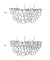
しかしながら、焼結セラミック上に感光性レジストを塗布して露光現像によりパターニングを行った場合、その後にめっき形成を行っても、均一にめっきが形成されず、めっき析出不良を発生する場合がある。その原因について本発明者らが鋭意検討したところによると、焼結セラミック上に感光性レジストを塗布して露光現像によりパターニングを行っても、焼結セラミックの表面形状影響から、図9に示すように、焼結セラミックの粒子a間の隙間に僅かなレジスト残りrが存在して十分に除去されず、このため、レジストを除去したはずの部分においても、残留レジストによるめっき析出を抑制する作用が影響してめっき析出不良を発生することがわかった。 However, when a photosensitive resist is applied onto the sintered ceramic and patterning is performed by exposure and development, even if plating is performed thereafter, plating is not uniformly formed, and plating deposition defects may occur. As a result of intensive studies by the present inventors on the cause, even if a photosensitive resist is applied on the sintered ceramic and patterned by exposure and development, the surface shape of the sintered ceramic has an effect, as shown in FIG. In addition, a slight resist residue r exists in the gaps between the sintered ceramic particles a and is not sufficiently removed. Therefore, even in the portion where the resist should have been removed, the effect of suppressing plating deposition due to the residual resist is exerted. It was found that plating deposition defects occurred due to the influence.
そこで、本発明の課題は、焼結セラミック上に感光性レジストを塗布して露光現像によりパターニングを行うことにより選択的にめっきを形成する際に、残留レジストに起因するめっき析出不良を発生することなく、均一にめっき形成を行うことのできるめっき形成方法を提供することにある。 Therefore, an object of the present invention is to generate plating deposition defects due to residual resist when selectively forming a plating by applying a photosensitive resist on a sintered ceramic and performing patterning by exposure and development. And a plating forming method capable of uniformly forming a plating.
また、本発明の他の課題は、インクジェットヘッドを構成する焼結セラミック上に感光性レジストを塗布して露光現像によりパターニングを行うことにより選択的にめっきによる電極を形成する際に、残留レジストに起因するめっき析出不良を発生することなく、均一にめっき形成を行うことのできるインクジェットヘッドの電極形成方法を提供することにある。 Another object of the present invention is to apply a photosensitive resist on a sintered ceramic constituting an ink jet head and perform patterning by exposure and development to form a residual resist when selectively forming electrodes by plating. It is an object of the present invention to provide an electrode forming method for an ink jet head capable of uniformly forming a plating without causing a defective plating deposition.
本発明の他の課題は、以下の記載により明らかとなる。 Other problems of the present invention will become apparent from the following description.
上記課題は、以下の各発明によって解決される。 The above problems are solved by the following inventions.
請求項1記載の発明は、焼結セラミック上に選択的にめっきを形成する方法であって、前記焼結セラミックのめっき形成面に感光性レジストを塗布した後、前記感光性レジストの露光・現像を行うことにより、めっき形成が必要な部分の焼結セラミックを露出させ、めっき形成が不要な部分の焼結セラミックを前記感光性レジストにより被覆された状態とし、前記焼結セラミック表面を酸性エッチング液で、前記焼結セラミックの平均粒子径の1/10倍以上2倍以下の深さの範囲でエッチングを行い、前記エッチング後の焼結セラミック表面にめっき触媒を付与した後、少なくともNiを含むめっきによりめっき形成を行うことを特徴とする焼結セラミック上に選択的にめっきを形成する方法である。
The invention according to
請求項2記載の発明は、前記めっきは、NiBめっき又はNiPめっきであることを特徴とする請求項1記載の焼結セラミック上に選択的にめっきを形成する方法である。
The invention according to
請求項3記載の発明は、インクジェットヘッドを構成する焼結セラミック上にめっきによって電極を形成するインクジェットヘッドの電極形成方法であって、前記焼結セラミックの電極形成面に感光性レジストを塗布した後、前記感光性レジストの露光・現像を行うことにより、電極形成が必要な部分の焼結セラミックを露出させ、電極形成が不要な部分の焼結セラミックを前記感光性レジストにより被覆された状態とし、前記焼結セラミック表面を酸性エッチング液で、前記焼結セラミックの平均粒子径の1/10倍以上2倍以下の深さの範囲でエッチングを行い、前記エッチング後の焼結セラミック表面にめっき触媒を付与した後、少なくともNiを含むめっきにより電極形成を行うことを特徴とするインクジェットヘッドの電極形成方法である。
The invention according to
請求項4記載の発明は、前記めっきは、NiBめっき又はNiPめっきであることを特徴とする請求項3記載のインクジェットヘッドの電極形成方法である。
The invention according to claim 4 is the electrode forming method for an ink jet head according to
以下、本発明の実施の形態について説明する。 Embodiments of the present invention will be described below.
本発明において、焼結セラミックとは、粉末の金属酸化物、硫化物等を融点以下または部分的融点の程度の加熱して強固な結合体としたものをいう。例えば、アルミナ、シリカ、チタニア等、各種金属酸化物、窒化珪素、窒化ホウ素、炭化珪素といった粉末を用いて作成される。特に、インクジェットヘッドを構成するアクチュエータとして用いられる圧電材料としての焼結セラミックとしては、PZT(ジルコニウム酸チタン酸鉛)、PLZT(ジルコニウム酸チタン酸鉛ランタン)等のセラミックで、主にPbOx、ZrOx、TiOxの混合微結晶体に、ソフト化剤又はハード化剤として知られる微量の金属酸化物、例えばNb、Zn、Mg、Sn、Ni、La、Cr等の酸化物を含むものが好ましい。中でもPZTは、充填密度が大きく、圧電性定数が大きく、加工性が良いので、インクジェットヘッドのアクチュエータとして好ましく使用できる。 In the present invention, the sintered ceramic means a powdered metal oxide, sulfide or the like heated to a melting point or lower or a partial melting point to form a strong bonded body. For example, it is prepared using powders such as various metal oxides such as alumina, silica, and titania, silicon nitride, boron nitride, and silicon carbide. Particularly, as a sintered ceramic as a piezoelectric material used as an actuator constituting an inkjet head, ceramics such as PZT (lead zirconate titanate) and PLZT (lead lanthanum zirconate titanate), mainly PbOx, ZrOx, It is preferable that the mixed microcrystal of TiOx contains a trace amount of metal oxide known as a softening agent or hardening agent, for example, an oxide such as Nb, Zn, Mg, Sn, Ni, La, or Cr. Among them, PZT can be preferably used as an actuator for an ink jet head because it has a high packing density, a large piezoelectric constant, and good workability.
焼結セラミックをこのようなインクジェットヘッドを構成するアクチュエータとして用いる場合、その平均粒子径は1〜8μmが好ましい。1μmより小さいと十分な感度が得られない。また、8μmより大きいと機械加工品質のばらつきが大きくなり好ましくない。 When the sintered ceramic is used as an actuator constituting such an ink jet head, the average particle diameter is preferably 1 to 8 μm. If it is smaller than 1 μm, sufficient sensitivity cannot be obtained. On the other hand, if it is larger than 8 μm, the variation in machining quality becomes large, which is not preferable.
そこで、焼結セラミックからなるインクジェットヘッドのアクチュエータにめっきにより電極形成を行う場合について、図面を用いて説明する。 Therefore, the case where electrodes are formed by plating on an actuator of an inkjet head made of sintered ceramic will be described with reference to the drawings.
図1〜図6は、インクジェットヘッドのアクチュエータにめっきにより電極形成を行う方法を説明する説明図である。 FIGS. 1-6 is explanatory drawing explaining the method of forming an electrode by plating to the actuator of an inkjet head.
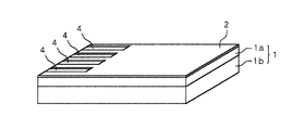
図1において、1はインクジェットヘッドのアクチュエータである。ここでは、PZT粉末を成型焼結した薄板のPZT板1aと厚板のPZT板1bとをそれぞれ分極処理し、その分極方向が反対となるようにエポキシ系接着剤等の接着剤により接着することで積層体を構成している。
In FIG. 1,
このようにPZT板1a、1bが積層されたアクチュエータ1の薄板のPZT板1aの上面に、感光性レジストを塗布し、レジスト膜2を形成する。
Thus, a photosensitive resist is applied to the upper surface of the thin PZT plate 1a of the
一般に、感光性レジストには、アルカリ可溶性樹脂、キノンジアジド化合物、めっき析出妨害成分等が含まれている。アルカリ可溶性樹脂には、ノボラック樹脂、アセトン−ピロガノール樹脂、ポリヒドロキシスチレン樹脂、アクリル樹脂等が用いられるが、中でも、本発明では、後工程において、後述する酸性のエッチング液を用いてエッチング処理を行うことから、ノボラック樹脂を用いたものが好ましく、具体的には、キノンジアジド化合物を感光材料としてノボラック樹脂を30%以上含有するポジ型レジストが好ましい。このような感光性レジストとしては、東京応化工業社製のOFPR800、P−LA100、P−HA100、N−CA500等が挙げられる。 In general, a photosensitive resist contains an alkali-soluble resin, a quinonediazide compound, a plating deposition-inhibiting component, and the like. As the alkali-soluble resin, a novolak resin, an acetone-pyroganol resin, a polyhydroxystyrene resin, an acrylic resin, or the like is used. In particular, in the present invention, an etching process is performed using an acidic etchant described later in the subsequent process. Therefore, those using novolak resin are preferable, and specifically, a positive resist containing 30% or more of novolak resin using a quinonediazide compound as a photosensitive material is preferable. Examples of such a photosensitive resist include OFPR800, P-LA100, P-HA100, and N-CA500 manufactured by Tokyo Ohka Kogyo Co., Ltd.
感光性レジストの要求特性は、めっき液及びめっき前の処理液に対する耐性が必要で、加えて、レジスト上へのめっき析出を妨害する特性が必要である。これらの特性を備えた上記組成のレジストが本発明には適している。本発明におけるめっき膜形成には、めっき形成部分と非形成部分との間で高い選択性が得られることで感光性レジスト上への異常めっき膜の形成等が改善され、適切な感光性レジストとなる。 The required characteristics of the photosensitive resist are required to have resistance to the plating solution and the treatment solution before plating, and in addition, the characteristics to hinder plating deposition on the resist are required. A resist having the above composition and having these characteristics is suitable for the present invention. In the plating film formation in the present invention, the formation of an abnormal plating film on the photosensitive resist is improved by obtaining high selectivity between the plating forming part and the non-forming part, and an appropriate photosensitive resist and Become.
この感光性レジストによるレジスト膜2の乾燥時の膜厚は、1〜10μmとすることが好ましい。1μmよりも薄いと被覆が不十分な場合があり、また、10μmよりも厚いと露光後の現像性が悪化するので好ましくない。より好ましくは2〜6μmとすることである。
The dry film thickness of the
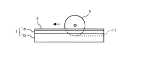
次いで、図2に示すように、感光性レジスト2の上面に、電極形成する部分としない部分、すなわちめっき形成する部分としない部分とを区別するよう形成されたフォトマスク3を載せる。フォトマスク3は、透明な石英板31にクロム蒸着によりパターニングを行ってマスク部32を形成したポジ型のフォトマスクである。このフォトマスク3の上から紫外線照射により露光し、現像液に浸漬して現像する。これにより、図3に示すように、フォトマスク3のマスク部32によって覆われて露光されなかった部分は現像時に消滅してアクチュエータ1の表面が露出し、露光された部分はレジスト膜2が残存する。現像時にレジスト膜2が消滅した部分はそれぞれ電極形成部4となる。
Next, as shown in FIG. 2, a
次いで、図4に示すように、このアクチュエータ1に対し、レジスト膜2形成面からダイシングソー5を用いて、厚板のPZT板1bの中途部まで至る深さの溝を電極形成部4と同数研削することによって、複数の互いに平行なチャネル11を並設する。このとき、各チャネル11は、アクチュエータ1表面の上記各電極形成部4とは反対端側から、それぞれ各電極形成部4にまで至る溝を研削することにより形成される。これにより、図5に示すように、各チャネル11内と上記各電極形成部4とを除くアクチュエータ1の表面のみがレジスト膜2で覆われた状態となる。なお、本実施形態では、アクチュエータ1に4本の電極形成部4を形成し、従って、4本のチャネル11を研削するものを示しているが、チャネル11の数は限定されない。
Next, as shown in FIG. 4, the
その後、このアクチュエータ1を酸性エッチング液に浸漬し、アクチュエータ1の表面をエッチングする。
Thereafter, the
エッチングに使用される液は、フッ化水素酸、酸性フッ化アンモニウム溶液、ホウフッ酸、ホウフッ酸金属塩、燐酸、硝酸、硫酸、塩酸、クロム酸等が挙げられ、これらを単独で用いてもよいし、これらのうちの複数を組合せるようにしてもよい。中でも、酸性フッ化アンモニウムと硝酸を組合せたものや、ホウフッ酸を使用したものが好ましい。 Examples of the liquid used for etching include hydrofluoric acid, acidic ammonium fluoride solution, borofluoric acid, borofluoric acid metal salt, phosphoric acid, nitric acid, sulfuric acid, hydrochloric acid, chromic acid and the like, and these may be used alone. However, a plurality of these may be combined. Among these, a combination of acidic ammonium fluoride and nitric acid and a borofluoric acid are preferable.
このような酸性エッチング液に浸漬することで、電極形成部4に露出している焼結セラミック表面が削られるが、本発明において、この酸性エッチング液によるエッチングは、アクチュエータ1を構成している焼結セラミックの平均粒子径の1/10倍以上2倍以下の深さの範囲で行う。図7(a)は焼結セラミックの平均粒子径の1/10倍の深さでエッチングを行った場合の様子を示し、(b)は焼結セラミックの平均粒子径の2倍の深さでエッチングを行った場合の様子を示している。図中、aはセラミック粒子、rは残留レジストを示しており、斜線部分はエッチング領域を示している。
By immersing in such an acidic etching solution, the surface of the sintered ceramic exposed to the electrode forming portion 4 is scraped. In the present invention, the etching with the acidic etching solution is a process that forms the
基材の洗浄とめっき膜の密着性を目的としてエッチングを行うことにより表面を粗面化することは知られているが、この場合はせいぜい平均粒子径の1/10未満のエッチングで十分であると考えられており、レジストの残留の問題については全く考慮されていなかった。しかし、本発明のように、レジストを用いたパターニングを行う場合に平均粒子径の1/10倍以上2倍以下の深さの範囲でエッチングすることによって、レジストの残留を防止することができる。すなわち、同図に示すように、酸性エッチング液によって焼結セラミックの平均粒子径の1/10倍以上2倍以下の深さの範囲でエッチングすることにより、露光・現像処理によっては除去しきれなかった焼結セラミック粒子間の残留レジストrは除去される。 Although it is known that the surface is roughened by etching for the purpose of cleaning the substrate and adhesion of the plating film, in this case, etching of less than 1/10 of the average particle diameter is sufficient. The problem of residual resist was not considered at all. However, as in the present invention, when patterning using a resist is performed, the remaining of the resist can be prevented by etching in a depth range of 1/10 to 2 times the average particle diameter. In other words, as shown in the figure, by etching in an acid etching solution within a depth range of 1/10 times or more and 2 times or less of the average particle diameter of the sintered ceramic, it cannot be completely removed by exposure / development processing. Residual resist r between the sintered ceramic particles is removed.
エッチング深さが1/10倍未満さでは、焼結セラミック粒子a間の残留レジストrをエッチングによって除去しきることができず、残留レジストrによってめっき析出不良を発生させる原因となる。また、2倍よりも深くなると、レジスト被覆部分の下をエッチングする状況になり、電極幅が設計値よりも大きくなって、FPC(フレキシブルプリント基板)接合時の短絡不良が増大することや、レジストの部分的な剥離が発生して周りを汚染することによるめっき析出不良が発生する場合がある。より好ましくは1/5倍以上1倍以下の深さとすることである。 When the etching depth is less than 1/10 times, the residual resist r between the sintered ceramic particles a cannot be removed by etching, and the residual resist r causes plating deposition failure. Moreover, when it becomes deeper than twice, it will be in the situation which etches under a resist coating part, an electrode width will become larger than a design value, the short circuit defect at the time of FPC (flexible printed circuit board) joining will increase, In some cases, plating deposition defects may occur due to contamination of the surrounding area due to partial peeling. More preferably, the depth is 1/5 or more and 1 or less.
エッチングの深さは、酸性エッチング液への浸漬時間を適宜調整することにより制御される。 The depth of etching is controlled by appropriately adjusting the immersion time in the acidic etching solution.
かかるエッチング処理の後、アクチュエータ1の表面にめっき触媒を付与する。めっき触媒は、電極形成部4となる焼結セラミック表面へのめっきの析出を効率良く行うための前処理として行われ、例えば無電解めっきによる場合は、触媒核となるパラジウム(Pd)を吸着させるものが好ましく用いられる。
After the etching process, a plating catalyst is applied to the surface of the
めっき触媒の付与の後、電極形成部4にめっきを形成する。すなわち、アクチュエータ1をめっき液に浸漬し、アクチュエータ1の表面にめっき膜を析出させる。
After application of the plating catalyst, plating is formed on the electrode forming portion 4. That is, the
ここで使用されるめっき金属は、少なくともニッケル(Ni)を含んでいる。少なくともNiを含むのは、比較的耐食性が高いことと、はんだ付き性、ワイヤボンディング、ACF(異方性導電フィルム)接合といった電極接合性が良いこと、基材との膜付き性が良いこと等が理由に挙げられる。また、このようなNiを含むめっき上に金(Au)めっきを施す等の多層めっきも容易となる利点がある。 The plating metal used here contains at least nickel (Ni). At least Ni is contained because of its relatively high corrosion resistance, good solderability, electrode bonding properties such as wire bonding and ACF (anisotropic conductive film) bonding, and good film adhesion to the substrate. Can be cited as the reason. Further, there is an advantage that multilayer plating such as gold (Au) plating on the plating containing Ni is easy.
Niめっきの種類としては、ホウ素(B)を含有するNiBめっき、りん(P)を含有するNiPめっきが好ましく、特に電気的抵抗が低い点からNiBめっきが好ましい。NiBめっきとNiPめっきとを積層して用いてもよい。 As the type of Ni plating, NiB plating containing boron (B) and NiP plating containing phosphorus (P) are preferable, and NiB plating is particularly preferable from the viewpoint of low electrical resistance. NiB plating and NiP plating may be laminated and used.
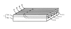
かかるめっき処理の後、アクチュエータ1の表面のレジスト膜2を剥離すると、図6に示すように、焼結セラミックが露出した電極形成部4のみに無電解めっきによるめっき金属が析出し、これによりアクチュエータ1の表面に電極6が選択的に形成される。なお、このとき、アクチュエータ1の両側面、底面、前及び後端面にも析出した不要なめっきは研磨することにより除去すればよい。
After the plating process, when the resist
その後、かかるアクチュエータ1を用いてインクジェットヘッドを作成するには、図8に示すように、アクチュエータ1の上面に、各チャネル11の後端部を残して該チャネル11の上方を覆うようにカバー基板7を接着剤を用いて接着し、該カバー基板7の前端面とアクチュエータ1の前端面とに亘って、各チャネル11に対応するノズル孔8aが開穿されたノズルプレート8を接着剤を用いて接着する。更にカバー基板7の上面に、各チャネル11内にインクを供給するインク供給室を構成するマニホールド9を接着剤を用いて接着すると共に、アクチュエータ1の上面に形成された各電極6に、駆動回路と電気的に接続される配線がパターン形成されたFPC10をACF等を用いて接合する。
Thereafter, in order to create an ink jet head using such an
以上の実施形態は、インクジェットヘッドを構成する焼結セラミック上に電極を形成する場合について例示したが、本発明は焼結セラミック上に感光性レジストを用いて露光・現像することにより、選択的にめっきを形成する場合に適用可能であり、これによりめっき形成部分に析出不良のない均一なめっきを形成することができる。 In the above embodiment, the electrode is formed on the sintered ceramic constituting the ink jet head. However, the present invention is selectively performed by exposing and developing the photosensitive resist on the sintered ceramic. The present invention can be applied to the case where plating is formed, whereby uniform plating with no precipitation failure can be formed in the plating formation portion.
また、特にインクジェットヘッドの電極形成やセラミック基板上に微細な電極による配線パターンを形成する場合等のように、焼結セラミックの基板上にめっきによる電極を微細なピッチで形成する場合には、各電極のピッチが狭くなるに従って、隣接する電極同士の短絡等を避けるため、自ずと形成可能なめっき厚が制限されるようになる。このため、めっき厚が薄くなる程、焼結セラミック上に現像処理によって除去しきれずに残量するレジストの影響を受け易くなり、めっき析出不良の発生がより多く見られるようになる。 In addition, when forming electrodes by plating on a sintered ceramic substrate at a fine pitch, such as when forming an electrode of an inkjet head or forming a wiring pattern with fine electrodes on a ceramic substrate, etc. As the pitch of the electrodes becomes narrower, the plating thickness that can be formed naturally is limited in order to avoid short circuits between adjacent electrodes. For this reason, as the plating thickness becomes thinner, it becomes more susceptible to the resist remaining on the sintered ceramic that cannot be completely removed by development processing, and the occurrence of plating deposition defects is more frequently observed.
従って、本発明においては、このように焼結セラミック上に電極を形成する場合の各電極のピッチが200μm以下、より好ましくは150μm以下のピッチで形成される場合に顕著な効果を発揮するものとなる。なお、このピッチは、隣接する電極の中心間距離である。電極の幅や電極と電極の間の距離はその1/2となる。 Therefore, in the present invention, when the electrodes are formed on the sintered ceramic in this way, the pitch of each electrode is 200 μm or less, more preferably 150 μm or less. Become. This pitch is the distance between the centers of adjacent electrodes. The width of the electrode and the distance between the electrodes are ½ of that.
また、同様に、めっき厚が薄いと残量レジストの影響を受け易くなることから、本発明においては、焼結セラミック上に形成されるめっき厚が5μm以下、より好ましくは3μm以下の薄めっきを形成する場合に顕著な効果を発揮するものとなる。 Similarly, if the plating thickness is thin, it is likely to be affected by the remaining resist. Therefore, in the present invention, a thin plating with a thickness of 5 μm or less, more preferably 3 μm or less, formed on the sintered ceramic is used. When it is formed, a remarkable effect is exhibited.
以下、実施例によって本発明の効果を例証する。
(実施例1)
住友エレクトロデバイス社製PZT粉末(平均粒子径:2μm)をそれぞれ成型焼結した薄板のPZT板と厚板のPZT板を分極処理し、その分極方向が反対となる向きで接着剤貼付することにより積層したアクチュエータを用意した。
Hereinafter, the effect of the present invention is illustrated by examples.
(Example 1)
By polarizing a thin PZT plate and a thick PZT plate obtained by molding and sintering PZT powder (average particle size: 2 μm) manufactured by Sumitomo Electrodevices, respectively, and applying an adhesive so that the polarization direction is opposite A stacked actuator was prepared.
<レジスト処理工程>
アクチュエータにおける薄板のPZT板側の面に、東京応化社製の液体レジスト「OFPR800」をスピンコーターで、乾燥時の膜厚が4μm±2μmの厚さとなるように塗布した。
<Resist processing step>
A liquid resist “OFPR800” manufactured by Tokyo Ohka Co., Ltd. was applied to the surface of the thin plate of the actuator on the PZT plate side with a spin coater so that the film thickness when dried was 4 μm ± 2 μm.
塗布後、90℃30分間のプリベーク処理をし、電極形成部となるレジスト表面を覆うようにアクチュエータ上にフォトマスクを載せ、該フォトマスクを通して、200mW/cm2、365nmの紫外光を1分間照射した。 After coating, pre-bake treatment is performed at 90 ° C. for 30 minutes, a photomask is placed on the actuator so as to cover the resist surface as an electrode forming portion, and ultraviolet light of 200 mW / cm 2 and 365 nm is irradiated for 1 minute through the photomask. did.
その後、東京応化社製の現像液「NMD−3」に2分間浸漬して現像し、図3で示したように、アクチュエータの表面に選択的にレジストが除去された電極形成部を形成した。その後、このアクチュエータを100℃で1時間のポストベークをした。 Thereafter, the film was immersed in a developer “NMD-3” manufactured by Tokyo Ohka Kogyo Co., Ltd. for 2 minutes for development, and as shown in FIG. 3, an electrode forming portion where the resist was selectively removed was formed on the surface of the actuator. Thereafter, this actuator was post-baked at 100 ° C. for 1 hour.
<溝形成工程>
レジスト処理後のアクチュエータのレジスト処理面側からダイシングソーにより、電極形成部チャネルとなる溝加工を行った。これにより、図5に示したように、各チャネル内と各電極形成部とを除くアクチュエータの表面のみがレジスト膜で覆われた状態となる。なお、チャネル幅は40μm、ピッチは85μmで、450本のチャネルを各々平行に並列形成した。
<Groove formation process>
A groove serving as an electrode forming portion channel was formed by a dicing saw from the resist processing surface side of the actuator after the resist processing. Thereby, as shown in FIG. 5, only the surface of the actuator excluding the inside of each channel and each electrode forming portion is covered with the resist film. The channel width was 40 μm, the pitch was 85 μm, and 450 channels were formed in parallel.
<エッチング工程>
溝加工後のアクチュエータを、pH3の酸性フッ化アンモニウム溶液(15%)に揺動しながら浸漬した。この浸漬処理の後、続いて、硝酸(30%)溶液に揺動しながら浸漬した。このエッチング処理の時間及びエッチング深さ(エッチング量)及びその平均粒子径に対する比率は、表1に示す通りである。
<Etching process>
The grooved actuator was immersed in a
<触媒付与工程>
エッチング処理後、アクチュエータをSnCl2の4%溶液(HClでpH1に調整)に揺動しながら30秒間浸漬した。この浸漬処理の後、続いて、PdCl2の0.04%溶液に揺動しながら30秒間浸漬し、アクチュエータの焼結セラミックが露出した部分にめっき触媒としてのパラジウム触媒を付与した。
<Catalyst application process>
After the etching process, the actuator was immersed for 30 seconds in a 4% SnCl 2 solution (adjusted to
<めっき成膜工程>
触媒付与後のアクチュエータを、奥野製薬社製めっき液「ニボロン70」を60℃、pH6.5に調整した溶液に、揺動しながら10分間浸漬し、NiBめっき成膜処理をした。このときのめっき膜の厚みは2.0μmであった。
<Plating film formation process>
The actuator after applying the catalyst was immersed for 10 minutes in a solution in which a plating solution “Niboron 70” manufactured by Okuno Pharmaceutical Co., Ltd. was adjusted to 60 ° C. and pH 6.5, and subjected to NiB plating film formation. The thickness of the plating film at this time was 2.0 μm.
<レジスト剥離工程>
めっき膜形成後のアクチュエータをアセトン溶液に浸漬して、アクチュエータ表面のレジストを溶解剥離し、洗浄し、図6に示したように、各チャネル内及びこれに繋がるアクチュエータ表面にめっき電極が形成されたアクチュエータを作成した。
<Resist stripping process>
The actuator after plating film formation was immersed in an acetone solution, the resist on the actuator surface was dissolved and peeled off, washed, and as shown in FIG. 6, plating electrodes were formed in each channel and on the actuator surface connected thereto. An actuator was created.
(実施例2)
エッチングの処理時間を表1の通り変えた以外は実施例1と同一とした。
(Example 2)
Example 1 was the same as Example 1 except that the etching processing time was changed as shown in Table 1.
(実施例3)
エッチング工程において、処理液を酸性フッ化アンモニウム+硝酸に代えて、ホウフッ酸(1%)を用い、表1の通りの時間でアクチュエータを揺動しながら浸漬処理した以外は実施例1と同一とした。
(Example 3)
In the etching process, the treatment solution was replaced with acidic ammonium fluoride + nitric acid, and borofluoric acid (1%) was used. Except that the immersion treatment was performed while the actuator was swung for the time shown in Table 1, the same as in Example 1. did.
(実施例4)
エッチング工程において、処理液を酸性フッ化アンモニウム+硝酸に代えて、ホウフッ酸(5%)を用い、表1の通りの時間でアクチュエータを揺動しながら浸漬処理した以外は実施例1と同一とした。
Example 4
In the etching process, the treatment solution was replaced with acidic ammonium fluoride + nitric acid, and borofluoric acid (5%) was used. did.
(比較例1、2)
エッチングの処理時間をそれぞれ表1の通り変えた以外は実施例1と同一とした。
(Comparative Examples 1 and 2)
Example 1 was the same as Example 1 except that the etching processing time was changed as shown in Table 1.
(評価)
アクチュエータの表面に形成されためっき電極について目視観察及び導通テストを行い、以下の基準により評価した。
◎:めっき析出不良は認められず、表面が均一に形成された。
○:めっき析出不良は認められなかった。
△:部分的にめっき析出不良が発生しているが、導通可能であった。
×:めっき析出不良が発生し、導通不可であった。
(Evaluation)
Visual observation and continuity test were performed on the plated electrode formed on the surface of the actuator, and the following criteria were evaluated.
(Double-circle): The plating deposition defect was not recognized but the surface was formed uniformly.
A: No plating deposition failure was observed.
(Triangle | delta): Although plating deposit defect has generate | occur | produced partially, it was able to conduct | electrically_connect.
X: Plating deposition failure occurred and conduction was not possible.
その結果を表1に示す。 The results are shown in Table 1.

なお、比較例2では、めっき析出不良及び導通不良は発生しなかったが、めっき幅太りが発生したことにより、隣接する電極同士の短絡が発生した。 In Comparative Example 2, neither plating deposition failure nor conduction failure occurred, but a short circuit between adjacent electrodes occurred due to the occurrence of thickening of the plating width.
1:アクチュエータ
1a:薄板のPZT板
1b:厚板のPZT板
11:チャネル
2:レジスト膜
3:フォトマスク
4:電極形成部
5:ダイシングソー
6:電極
7:カバー基板
8:ノズルプレート
8a:ノズル孔
9:マニホールド
10:FPC
1: Actuator 1a:
Claims (4)
Priority Applications (1)
| Application Number | Priority Date | Filing Date | Title |
|---|---|---|---|
| JP2003387162A JP2005146367A (en) | 2003-11-17 | 2003-11-17 | Method for selectively performing plating on sintered ceramic, and method for forming electrode of ink jet head |
Applications Claiming Priority (1)
| Application Number | Priority Date | Filing Date | Title |
|---|---|---|---|
| JP2003387162A JP2005146367A (en) | 2003-11-17 | 2003-11-17 | Method for selectively performing plating on sintered ceramic, and method for forming electrode of ink jet head |
Publications (1)
| Publication Number | Publication Date |
|---|---|
| JP2005146367A true JP2005146367A (en) | 2005-06-09 |
Family
ID=34694623
Family Applications (1)
| Application Number | Title | Priority Date | Filing Date |
|---|---|---|---|
| JP2003387162A Pending JP2005146367A (en) | 2003-11-17 | 2003-11-17 | Method for selectively performing plating on sintered ceramic, and method for forming electrode of ink jet head |
Country Status (1)
| Country | Link |
|---|---|
| JP (1) | JP2005146367A (en) |
Cited By (3)
| Publication number | Priority date | Publication date | Assignee | Title |
|---|---|---|---|---|
| JP2011073459A (en) * | 2011-01-17 | 2011-04-14 | Toshiba Tec Corp | Method for manufacturing inkjet printer head |
| JP2014184633A (en) * | 2013-03-22 | 2014-10-02 | Seiko Epson Corp | Passage unit, liquid jet head, liquid jet apparatus, and manufacturing method of passage unit |
| JP7185454B2 (en) | 2018-09-14 | 2022-12-07 | エスアイアイ・プリンテック株式会社 | HEAD CHIP, LIQUID JET HEAD, LIQUID JET RECORDING APPARATUS, AND HEAD CHIP MANUFACTURING METHOD |
-
2003
- 2003-11-17 JP JP2003387162A patent/JP2005146367A/en active Pending
Cited By (3)
| Publication number | Priority date | Publication date | Assignee | Title |
|---|---|---|---|---|
| JP2011073459A (en) * | 2011-01-17 | 2011-04-14 | Toshiba Tec Corp | Method for manufacturing inkjet printer head |
| JP2014184633A (en) * | 2013-03-22 | 2014-10-02 | Seiko Epson Corp | Passage unit, liquid jet head, liquid jet apparatus, and manufacturing method of passage unit |
| JP7185454B2 (en) | 2018-09-14 | 2022-12-07 | エスアイアイ・プリンテック株式会社 | HEAD CHIP, LIQUID JET HEAD, LIQUID JET RECORDING APPARATUS, AND HEAD CHIP MANUFACTURING METHOD |
Similar Documents
| Publication | Publication Date | Title |
|---|---|---|
| US8438729B2 (en) | Method of producing liquid discharge head | |
| JP2001068828A (en) | Wiring board and its manufacture | |
| WO1997046390A1 (en) | Ink jet head and method of manufacturing same | |
| JP2005146367A (en) | Method for selectively performing plating on sintered ceramic, and method for forming electrode of ink jet head | |
| JP2007331135A (en) | Electrode forming method and method for manufacturing inkjet head | |
| JP5980020B2 (en) | Manufacturing method of substrate for liquid discharge head | |
| JP4599132B2 (en) | Printed circuit board manufacturing method and printed circuit board | |
| US20050218110A1 (en) | Method for manufacturing wiring substrate and method for manufacturing electronic device | |
| JP2006161116A (en) | Electrode forming method by electroless plating, and method for manufacturing ink jet head | |
| JP2001111201A (en) | Method of manufacturing wiring board and wiring board using the same | |
| JPH08267768A (en) | Manufacture of ink jet printer head | |
| JP2006346962A (en) | Pattern formation method and liquid droplet jet head | |
| JP2002172789A (en) | Method of manufacturing ink jet head | |
| JP2000103062A (en) | Fine shape part and its manufacture | |
| JP2002111185A (en) | Wiring circuit board with bumps and method of manufacturing the same | |
| JP2008016507A (en) | Process for producing electric wiring | |
| JP2007269009A (en) | Liquid discharge head and manufacturing method therefor | |
| JP3951137B2 (en) | Wiring board manufacturing method and electronic device manufacturing method | |
| JP3387352B2 (en) | Ink jet recording head, ink jet recording apparatus using the same, and method of manufacturing ink jet recording head | |
| JPH05504233A (en) | Printed circuit board and its manufacturing method | |
| JP2008251750A (en) | Forming method of bump for electric connection | |
| JP2005103881A (en) | Manufacturing method for inkjet head | |
| JP2003182069A (en) | Ink jet head and its producing method | |
| JP3969140B2 (en) | Plating method and plated product | |
| JP4439963B2 (en) | Electrodeposition film forming method and semiconductor device |