JP2005140976A - Display device - Google Patents
Display device Download PDFInfo
- Publication number
- JP2005140976A JP2005140976A JP2003377069A JP2003377069A JP2005140976A JP 2005140976 A JP2005140976 A JP 2005140976A JP 2003377069 A JP2003377069 A JP 2003377069A JP 2003377069 A JP2003377069 A JP 2003377069A JP 2005140976 A JP2005140976 A JP 2005140976A
- Authority
- JP
- Japan
- Prior art keywords
- layer
- resin
- substrate
- display device
- inorganic barrier
- Prior art date
- Legal status (The legal status is an assumption and is not a legal conclusion. Google has not performed a legal analysis and makes no representation as to the accuracy of the status listed.)
- Granted
Links
- 239000000758 substrate Substances 0.000 claims abstract description 106
- 229920005989 resin Polymers 0.000 claims abstract description 71
- 239000011347 resin Substances 0.000 claims abstract description 71
- 229920003023 plastic Polymers 0.000 claims abstract description 62
- 239000000835 fiber Substances 0.000 claims abstract description 61
- 239000004033 plastic Substances 0.000 claims abstract description 57
- 230000004888 barrier function Effects 0.000 claims abstract description 55
- 239000004744 fabric Substances 0.000 claims abstract description 34
- 239000002131 composite material Substances 0.000 claims description 33
- 239000004973 liquid crystal related substance Substances 0.000 claims description 21
- 238000000034 method Methods 0.000 claims description 19
- 238000004519 manufacturing process Methods 0.000 claims description 14
- VYPSYNLAJGMNEJ-UHFFFAOYSA-N Silicium dioxide Chemical compound O=[Si]=O VYPSYNLAJGMNEJ-UHFFFAOYSA-N 0.000 claims description 4
- 230000008569 process Effects 0.000 claims description 3
- 235000012239 silicon dioxide Nutrition 0.000 claims description 2
- 239000000377 silicon dioxide Substances 0.000 claims description 2
- 238000007736 thin film deposition technique Methods 0.000 claims description 2
- 239000010408 film Substances 0.000 description 20
- 239000003365 glass fiber Substances 0.000 description 14
- 229910004298 SiO 2 Inorganic materials 0.000 description 11
- 239000000463 material Substances 0.000 description 8
- 239000011521 glass Substances 0.000 description 7
- 239000011159 matrix material Substances 0.000 description 6
- 239000003822 epoxy resin Substances 0.000 description 5
- 229920000647 polyepoxide Polymers 0.000 description 5
- 238000009941 weaving Methods 0.000 description 5
- 238000010438 heat treatment Methods 0.000 description 4
- 230000007246 mechanism Effects 0.000 description 4
- 238000009828 non-uniform distribution Methods 0.000 description 4
- 238000001771 vacuum deposition Methods 0.000 description 4
- 238000000151 deposition Methods 0.000 description 3
- 238000002347 injection Methods 0.000 description 3
- 239000007924 injection Substances 0.000 description 3
- 239000002759 woven fabric Substances 0.000 description 3
- QVGXLLKOCUKJST-UHFFFAOYSA-N atomic oxygen Chemical compound [O] QVGXLLKOCUKJST-UHFFFAOYSA-N 0.000 description 2
- 230000015572 biosynthetic process Effects 0.000 description 2
- 239000000945 filler Substances 0.000 description 2
- 230000008570 general process Effects 0.000 description 2
- 229910052760 oxygen Inorganic materials 0.000 description 2
- 239000001301 oxygen Substances 0.000 description 2
- 239000000126 substance Substances 0.000 description 2
- 229920005992 thermoplastic resin Polymers 0.000 description 2
- 229920001187 thermosetting polymer Polymers 0.000 description 2
- 239000013306 transparent fiber Substances 0.000 description 2
- 239000004695 Polyether sulfone Substances 0.000 description 1
- 239000004697 Polyetherimide Substances 0.000 description 1
- 239000004760 aramid Substances 0.000 description 1
- 229920003235 aromatic polyamide Polymers 0.000 description 1
- GDTBXPJZTBHREO-UHFFFAOYSA-N bromine Substances BrBr GDTBXPJZTBHREO-UHFFFAOYSA-N 0.000 description 1
- 229910052794 bromium Inorganic materials 0.000 description 1
- 238000005266 casting Methods 0.000 description 1
- 230000006835 compression Effects 0.000 description 1
- 238000007906 compression Methods 0.000 description 1
- 238000000748 compression moulding Methods 0.000 description 1
- 230000007547 defect Effects 0.000 description 1
- 238000009826 distribution Methods 0.000 description 1
- 238000001125 extrusion Methods 0.000 description 1
- 230000002349 favourable effect Effects 0.000 description 1
- 239000002657 fibrous material Substances 0.000 description 1
- 125000001153 fluoro group Chemical group F* 0.000 description 1
- 230000001771 impaired effect Effects 0.000 description 1
- 238000005470 impregnation Methods 0.000 description 1
- 238000001746 injection moulding Methods 0.000 description 1
- 239000012784 inorganic fiber Substances 0.000 description 1
- 238000000465 moulding Methods 0.000 description 1
- 239000004745 nonwoven fabric Substances 0.000 description 1
- 230000003287 optical effect Effects 0.000 description 1
- 238000000059 patterning Methods 0.000 description 1
- 230000035699 permeability Effects 0.000 description 1
- 239000005011 phenolic resin Substances 0.000 description 1
- 239000004417 polycarbonate Substances 0.000 description 1
- 229920000515 polycarbonate Polymers 0.000 description 1
- 229920006393 polyether sulfone Polymers 0.000 description 1
- 229920001601 polyetherimide Polymers 0.000 description 1
- 230000004044 response Effects 0.000 description 1
- 238000005096 rolling process Methods 0.000 description 1
- 239000003566 sealing material Substances 0.000 description 1
- 125000006850 spacer group Chemical group 0.000 description 1
- 125000001424 substituent group Chemical group 0.000 description 1
- 239000010409 thin film Substances 0.000 description 1
- 238000001721 transfer moulding Methods 0.000 description 1
Images


Classifications
-
- G—PHYSICS
- G02—OPTICS
- G02F—OPTICAL DEVICES OR ARRANGEMENTS FOR THE CONTROL OF LIGHT BY MODIFICATION OF THE OPTICAL PROPERTIES OF THE MEDIA OF THE ELEMENTS INVOLVED THEREIN; NON-LINEAR OPTICS; FREQUENCY-CHANGING OF LIGHT; OPTICAL LOGIC ELEMENTS; OPTICAL ANALOGUE/DIGITAL CONVERTERS
- G02F1/00—Devices or arrangements for the control of the intensity, colour, phase, polarisation or direction of light arriving from an independent light source, e.g. switching, gating or modulating; Non-linear optics
- G02F1/01—Devices or arrangements for the control of the intensity, colour, phase, polarisation or direction of light arriving from an independent light source, e.g. switching, gating or modulating; Non-linear optics for the control of the intensity, phase, polarisation or colour
- G02F1/13—Devices or arrangements for the control of the intensity, colour, phase, polarisation or direction of light arriving from an independent light source, e.g. switching, gating or modulating; Non-linear optics for the control of the intensity, phase, polarisation or colour based on liquid crystals, e.g. single liquid crystal display cells
- G02F1/133—Constructional arrangements; Operation of liquid crystal cells; Circuit arrangements
- G02F1/1333—Constructional arrangements; Manufacturing methods
- G02F1/133305—Flexible substrates, e.g. plastics, organic film
-
- H—ELECTRICITY
- H10—SEMICONDUCTOR DEVICES; ELECTRIC SOLID-STATE DEVICES NOT OTHERWISE PROVIDED FOR
- H10K—ORGANIC ELECTRIC SOLID-STATE DEVICES
- H10K50/00—Organic light-emitting devices
- H10K50/80—Constructional details
- H10K50/84—Passivation; Containers; Encapsulations
- H10K50/844—Encapsulations
-
- H—ELECTRICITY
- H10—SEMICONDUCTOR DEVICES; ELECTRIC SOLID-STATE DEVICES NOT OTHERWISE PROVIDED FOR
- H10K—ORGANIC ELECTRIC SOLID-STATE DEVICES
- H10K59/00—Integrated devices, or assemblies of multiple devices, comprising at least one organic light-emitting element covered by group H10K50/00
- H10K59/80—Constructional details
- H10K59/87—Passivation; Containers; Encapsulations
- H10K59/873—Encapsulations
-
- H—ELECTRICITY
- H10—SEMICONDUCTOR DEVICES; ELECTRIC SOLID-STATE DEVICES NOT OTHERWISE PROVIDED FOR
- H10K—ORGANIC ELECTRIC SOLID-STATE DEVICES
- H10K77/00—Constructional details of devices covered by this subclass and not covered by groups H10K10/80, H10K30/80, H10K50/80 or H10K59/80
- H10K77/10—Substrates, e.g. flexible substrates
-
- C—CHEMISTRY; METALLURGY
- C09—DYES; PAINTS; POLISHES; NATURAL RESINS; ADHESIVES; COMPOSITIONS NOT OTHERWISE PROVIDED FOR; APPLICATIONS OF MATERIALS NOT OTHERWISE PROVIDED FOR
- C09K—MATERIALS FOR MISCELLANEOUS APPLICATIONS, NOT PROVIDED FOR ELSEWHERE
- C09K2323/00—Functional layers of liquid crystal optical display excluding electroactive liquid crystal layer characterised by chemical composition
- C09K2323/05—Bonding or intermediate layer characterised by chemical composition, e.g. sealant or spacer
- C09K2323/051—Inorganic, e.g. glass or silicon oxide
-
- C—CHEMISTRY; METALLURGY
- C09—DYES; PAINTS; POLISHES; NATURAL RESINS; ADHESIVES; COMPOSITIONS NOT OTHERWISE PROVIDED FOR; APPLICATIONS OF MATERIALS NOT OTHERWISE PROVIDED FOR
- C09K—MATERIALS FOR MISCELLANEOUS APPLICATIONS, NOT PROVIDED FOR ELSEWHERE
- C09K2323/00—Functional layers of liquid crystal optical display excluding electroactive liquid crystal layer characterised by chemical composition
- C09K2323/06—Substrate layer characterised by chemical composition
-
- H—ELECTRICITY
- H10—SEMICONDUCTOR DEVICES; ELECTRIC SOLID-STATE DEVICES NOT OTHERWISE PROVIDED FOR
- H10K—ORGANIC ELECTRIC SOLID-STATE DEVICES
- H10K59/00—Integrated devices, or assemblies of multiple devices, comprising at least one organic light-emitting element covered by group H10K50/00
-
- Y—GENERAL TAGGING OF NEW TECHNOLOGICAL DEVELOPMENTS; GENERAL TAGGING OF CROSS-SECTIONAL TECHNOLOGIES SPANNING OVER SEVERAL SECTIONS OF THE IPC; TECHNICAL SUBJECTS COVERED BY FORMER USPC CROSS-REFERENCE ART COLLECTIONS [XRACs] AND DIGESTS
- Y02—TECHNOLOGIES OR APPLICATIONS FOR MITIGATION OR ADAPTATION AGAINST CLIMATE CHANGE
- Y02E—REDUCTION OF GREENHOUSE GAS [GHG] EMISSIONS, RELATED TO ENERGY GENERATION, TRANSMISSION OR DISTRIBUTION
- Y02E10/00—Energy generation through renewable energy sources
- Y02E10/50—Photovoltaic [PV] energy
- Y02E10/549—Organic PV cells
-
- Y—GENERAL TAGGING OF NEW TECHNOLOGICAL DEVELOPMENTS; GENERAL TAGGING OF CROSS-SECTIONAL TECHNOLOGIES SPANNING OVER SEVERAL SECTIONS OF THE IPC; TECHNICAL SUBJECTS COVERED BY FORMER USPC CROSS-REFERENCE ART COLLECTIONS [XRACs] AND DIGESTS
- Y02—TECHNOLOGIES OR APPLICATIONS FOR MITIGATION OR ADAPTATION AGAINST CLIMATE CHANGE
- Y02P—CLIMATE CHANGE MITIGATION TECHNOLOGIES IN THE PRODUCTION OR PROCESSING OF GOODS
- Y02P70/00—Climate change mitigation technologies in the production process for final industrial or consumer products
- Y02P70/50—Manufacturing or production processes characterised by the final manufactured product
-
- Y—GENERAL TAGGING OF NEW TECHNOLOGICAL DEVELOPMENTS; GENERAL TAGGING OF CROSS-SECTIONAL TECHNOLOGIES SPANNING OVER SEVERAL SECTIONS OF THE IPC; TECHNICAL SUBJECTS COVERED BY FORMER USPC CROSS-REFERENCE ART COLLECTIONS [XRACs] AND DIGESTS
- Y10—TECHNICAL SUBJECTS COVERED BY FORMER USPC
- Y10T—TECHNICAL SUBJECTS COVERED BY FORMER US CLASSIFICATION
- Y10T442/00—Fabric [woven, knitted, or nonwoven textile or cloth, etc.]
- Y10T442/20—Coated or impregnated woven, knit, or nonwoven fabric which is not [a] associated with another preformed layer or fiber layer or, [b] with respect to woven and knit, characterized, respectively, by a particular or differential weave or knit, wherein the coating or impregnation is neither a foamed material nor a free metal or alloy layer
- Y10T442/2926—Coated or impregnated inorganic fiber fabric
- Y10T442/2992—Coated or impregnated glass fiber fabric
-
- Y—GENERAL TAGGING OF NEW TECHNOLOGICAL DEVELOPMENTS; GENERAL TAGGING OF CROSS-SECTIONAL TECHNOLOGIES SPANNING OVER SEVERAL SECTIONS OF THE IPC; TECHNICAL SUBJECTS COVERED BY FORMER USPC CROSS-REFERENCE ART COLLECTIONS [XRACs] AND DIGESTS
- Y10—TECHNICAL SUBJECTS COVERED BY FORMER USPC
- Y10T—TECHNICAL SUBJECTS COVERED BY FORMER US CLASSIFICATION
- Y10T442/00—Fabric [woven, knitted, or nonwoven textile or cloth, etc.]
- Y10T442/30—Woven fabric [i.e., woven strand or strip material]
- Y10T442/3049—Including strand precoated with other than free metal or alloy
Landscapes
- Physics & Mathematics (AREA)
- Nonlinear Science (AREA)
- Optics & Photonics (AREA)
- Mathematical Physics (AREA)
- Chemical & Material Sciences (AREA)
- Crystallography & Structural Chemistry (AREA)
- General Physics & Mathematics (AREA)
- Liquid Crystal (AREA)
- Devices For Indicating Variable Information By Combining Individual Elements (AREA)
- Laminated Bodies (AREA)
- Electroluminescent Light Sources (AREA)
Abstract
Description
本発明は、プラスチック基板を備えた表示装置およびその製造方法に関し、特に、繊維充填系プラスチック基板を備えた表示装置に関する。 The present invention relates to a display device including a plastic substrate and a manufacturing method thereof, and more particularly to a display device including a fiber-filled plastic substrate.
近年、薄型、軽量で、且つ、消費電力が低いという特徴から、液晶表示装置や有機EL表示装置の携帯情報端末機器への利用が広がるにつれて、これらの表示装置の更なる軽量化、薄型化、耐衝撃性の向上などが強く望まれるようになっている。 In recent years, as the use of liquid crystal display devices and organic EL display devices for portable information terminal devices has expanded due to the characteristics of being thin, lightweight and low in power consumption, these display devices are further reduced in weight and thickness. Improvements in impact resistance are strongly desired.
そこで、従来使用されてきたガラス基板の代わりにプラスチック基板を用いるという対策が提案されている。しかしながら、樹脂材料をシート化したプラスチック基板を表示装置の基板に適用するためには、様々な課題がある。 Therefore, a countermeasure has been proposed in which a plastic substrate is used instead of the glass substrate that has been conventionally used. However, there are various problems in applying a plastic substrate in which a resin material is made into a sheet to a substrate of a display device.
最も大きな課題の1つは、プラスチック基板の線膨張率が大きいことである。ガラスの線膨張率は一般に数ppm/℃程度であるのに対し、プラスチックの線膨張率は、小さいものでも数十ppm/℃ある。線膨張率が大きいと、温度による寸法の変動が大きくなるため、高精度のパターニングを要求される、例えばTFTのような駆動素子の作製が困難である。また、TFTが形成される基板(単に「TFT基板」ということもある。)として従来のガラス基板を用い、対向基板にプラスチック基板を用いても、対向基板に形成されたカラーフィルタ(および/またはブラックマトリクス)と、TFT基板の画素電極との位置合わせが困難となる。 One of the biggest problems is that the linear expansion coefficient of the plastic substrate is large. The linear expansion coefficient of glass is generally about several ppm / ° C., whereas the linear expansion coefficient of plastic is several tens of ppm / ° C. even if it is small. When the linear expansion coefficient is large, the dimensional variation due to temperature increases, so that it is difficult to manufacture a driving element such as a TFT that requires high-precision patterning. Even if a conventional glass substrate is used as a substrate on which a TFT is formed (also simply referred to as a “TFT substrate”) and a plastic substrate is used as the counter substrate, a color filter (and / or It becomes difficult to align the black matrix) with the pixel electrode of the TFT substrate.
プラスチック基板の線膨張率を小さくし、寸法安定性を向上させるために、樹脂マトリクス中に充填材(フィラー)を混合した材料(複合材料)を用いてプラスチック基板を構成する方法も提案されている。本明細書において、複合材料から形成されたプラスチック基板を特に「複合基板(コンポジット基板)」ということもある。 In order to reduce the linear expansion coefficient of the plastic substrate and improve the dimensional stability, a method of configuring the plastic substrate using a material (composite material) in which a filler (filler) is mixed in a resin matrix has been proposed. . In the present specification, a plastic substrate formed from a composite material may be particularly referred to as a “composite substrate (composite substrate)”.
例えば、特許文献1には、ガラス繊維布に樹脂を含浸させて硬化することによって形成された複合基板を備える反射型導電性基板が開示されている。
For example,
また、特許文献2は、樹脂中に繊維を線状あるいは帯状に繊維同士が互いに接触しないように配置された複合基板を開示している。特許文献2によると、特許文献1に開示されている繊維布(織布)を充填した複合基板を用いると繊維布の繊維の織目や重なり目に起因した微小な凹凸が基板表面に生じ、表示品位の低下の原因となってしまうのに対し、上記構成とすることによって、平坦な表面の複合基板が得られる。
上記特許文献2にも記載されているように、ガラス繊維布を用いてプラスチック基板を形成すると、その表面に凹凸が形成される。また、特許文献2に記載されているプラスチック基板は作製が困難であり、また、作製できたとしても、例えば100nm以下のレベルまで凹凸を抑制することは困難である。
As described in
また、プラスチック基板の表面を平坦化するために、上記凹凸を有する表面に平坦化膜を形成する方法がある。平坦化膜を形成することによって、例えば凹凸を100nm以下のレベルまで抑制した平坦な表面を得ることができる。しかしながら、本発明者の検討によると、この平坦な表面上に無機バリア層を形成すると、無機バリア層の表面に100nm以上の凹凸が形成されることがある。無機バリア層は、空気中の水分および/または酸素に対するプラスチック基板のバリア性を向上するために設けられる。 In order to planarize the surface of the plastic substrate, there is a method of forming a planarization film on the surface having the irregularities. By forming the planarizing film, for example, a flat surface in which unevenness is suppressed to a level of 100 nm or less can be obtained. However, according to the study of the present inventor, when an inorganic barrier layer is formed on this flat surface, irregularities of 100 nm or more may be formed on the surface of the inorganic barrier layer. The inorganic barrier layer is provided in order to improve the barrier property of the plastic substrate against moisture and / or oxygen in the air.
本発明は、上記諸点に鑑みてなされたものであり、その主な目的は、無機バリア層を有し、且つ、表面の平坦性に優れたプラスチック基板を備えた表示装置を提供することにある。 The present invention has been made in view of the above-described points, and a main object thereof is to provide a display device including an inorganic barrier layer and a plastic substrate having excellent surface flatness. .
本発明の表示装置は、樹脂が含浸された繊維布を含む複合体層と、前記複合体層上に形成された無機バリア層と、前記無機バリア層上に形成された平坦化樹脂層とを有する第1プラスチック基板と、前記第1基板の前記平坦化樹脂層側に設けられた表示媒体層とを有することを特徴とする。 The display device of the present invention includes a composite layer including a fiber cloth impregnated with a resin, an inorganic barrier layer formed on the composite layer, and a planarizing resin layer formed on the inorganic barrier layer. And a display medium layer provided on the planarizing resin layer side of the first substrate.
ある実施形態において、前記表示媒体層を介して前記第1基板に対向するように配置された第2プラスチック基板を有し、前記第2基板は前記第1基板と同じ構成を有する。 In one embodiment, a second plastic substrate is disposed so as to face the first substrate with the display medium layer interposed therebetween, and the second substrate has the same configuration as the first substrate.
ある実施形態において、前記表示媒体層は、有機発光層を含む。 In one embodiment, the display medium layer includes an organic light emitting layer.
ある実施形態において、前記表示媒体層は、液晶層である。 In one embodiment, the display medium layer is a liquid crystal layer.
ある実施形態において、前記無機バリア層は、前記複合体層の前記表示媒体層に対向する領域の全体を覆う。 In one embodiment, the inorganic barrier layer covers the entire region of the composite layer facing the display medium layer.
本発明の表示装置の製造法は、上記いずれかの表示装置の製造方法であって、前記第1プラスチック基板を製造するプロセスが、樹脂が含浸された繊維布を含む複合体層を用意する工程と、前記複合体層の表面に薄膜堆積法を用いて、第1の温度で無機バリア層を形成する工程と、前記無機バリア層上に、前記第1の温度よりも低い第2の温度で前記平坦化樹脂層を形成する工程とを包含することを特徴とする。 The display device manufacturing method of the present invention is any of the above display device manufacturing methods, wherein the process of manufacturing the first plastic substrate is a step of preparing a composite layer including a fiber cloth impregnated with a resin. A step of forming an inorganic barrier layer at a first temperature using a thin film deposition method on the surface of the composite layer; and a second temperature lower than the first temperature on the inorganic barrier layer. Forming the planarizing resin layer.
ある実施形態において、前記第1の温度が200℃以上である。 In one embodiment, the first temperature is 200 ° C. or higher.
ある実施形態において、前記無機バリア層は、二酸化ケイ素を含む。 In one embodiment, the inorganic barrier layer includes silicon dioxide.
本発明による表示装置のプラスチック基板は、樹脂が含浸された繊維布を含む複合体層上に形成された無機バリア層の上に平坦化樹脂層が形成されているので、平坦化樹脂層上に無機バリア層を形成するための加熱処理工程において無機バリア層の表面に凹凸が形成されることが無く、平坦な表面を有している。従って、例えば液晶表示層を構成した場合も、プラスチック基板の表面の凹凸に起因するセル厚のむらが無く、高品位の表示を実現することができる。 In the plastic substrate of the display device according to the present invention, the planarizing resin layer is formed on the inorganic barrier layer formed on the composite layer including the fiber cloth impregnated with the resin. Irregularities are not formed on the surface of the inorganic barrier layer in the heat treatment step for forming the inorganic barrier layer, and the surface has a flat surface. Therefore, for example, even when a liquid crystal display layer is formed, high-quality display can be realized without unevenness of the cell thickness due to the unevenness of the surface of the plastic substrate.
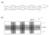
上述したように、本発明者は、所定の平坦性を有する複合基板の平坦化膜の表面上に無機バリア層を堆積すると、平坦性が損なわれ、無機バリア層の表面に凹凸が形成されるという現象を見出した。まず、図1および図2を参照しながら、この現象を説明する。 As described above, when the present inventor deposits an inorganic barrier layer on the surface of the planarization film of the composite substrate having a predetermined flatness, the flatness is impaired and irregularities are formed on the surface of the inorganic barrier layer. I found the phenomenon. First, this phenomenon will be described with reference to FIGS.
図1は、プラスチック基板に用いられる樹脂を含浸したガラス繊維布3の一部を模式的であり、図1(a)は断面図であり、図1(b)は平面図である。
FIG. 1 is a schematic view of a part of a
図1に示した樹脂含浸ガラス繊維布3は、ガラス繊維布1Sと、ガラス繊維布1Aを覆う樹脂層2とを有している。ガラス繊維布1Sは、複数のガラス繊維1を束ねた繊維束1Aを縦横に平織したものである。樹脂層2は、ガラス繊維布13を例えばエポキシ樹脂に含浸することによって形成されるので、ガラス繊維束1Aの表面を覆う薄膜として形成される。樹脂含浸ガラス繊維布3は、図1(a)に模式的に示したように、繊維束1Aが互いに重なる織り目に応じた凹凸を有する。
The resin-impregnated
例えば、繊維束1Aを構成する繊維1の直径は約10μmであり、繊維束1Aの幅は約200μmで、繊維束1Aの間のピッチは縦横いずれにおいても約500μmである。樹脂層2の厚さは、例えば約20μmである。この樹脂含浸繊維布1Sは、約500nmから600nmの程度の凹凸(うねり)を有している。
For example, the diameter of the
従来は、図2(a)に示すように、この樹脂含浸繊維布3の凹凸を平坦化するための平坦化樹脂層14が設けられている。平坦化層14を設けることによって、表面の凹凸は約100nm程度にまで低減される。
Conventionally, as shown in FIG. 2A, a
この平坦化樹脂層14の上に、空気中の水分および/または酸素に対するバリア性を向上するために、無機バリア層15が設けられる。SiO2を加熱成膜プロセス(例えば200℃で真空蒸着)で堆積することによって、厚さが約100nmの無機バリア層15を形成すると、得られたプラスチック基板10の表面(無機バリア層15の表面)は、図2(b)に模式的に示すように、凹凸の程度が約400nm程度にまで増大される。
An
図3に模式的に示すように、このプラスチック基板10と基板(例えばガラス基板)17との間に液晶層16を配置した液晶表示装置100を構成すると、プラスチック基板10の表面の凹凸の影響を受けて、液晶層16の厚さ(セル厚)に不均一な分布が形成される。液晶層16の厚さの不均一な分布は、リタデーションの不均一な分布となるので、表示むらとして観察される。
As schematically shown in FIG. 3, when the liquid
一旦平坦化された表面に再び凹凸が形成されるメカニズムを種々の実験結果に基づいて検討した。その結果、以下に説明するメカニズムであると考えるに至った。 The mechanism by which irregularities are formed again on the flattened surface was examined based on various experimental results. As a result, it came to consider that it is a mechanism demonstrated below.
図2(a)に示した平坦化樹脂層14上にSiO2を堆積する際に、基板(ここでは、樹脂含浸繊維布3およびその上に形成された平坦化樹脂層14のことを指す。)が例えば200℃に加熱される。基板内には、繊維1の体積分率が異なる領域が存在するので、熱膨張量に不均一な分布が形成される。すなわち、繊維1が多く存在する領域の熱膨張量が小さく、繊維1が少ない領域の熱膨張量は大きくなる。もちろん、繊維1が存在しない領域の熱膨張量が最も大きい。この熱膨張量の不均一分布によって基板(平坦化樹脂層14)の表面に凹凸が形成される。この凹凸が形成された表面上にSiO2が堆積されると、SiO2膜(無機バリア層)の表面は、下地の凹凸を反映した凹凸を有したものとなる。SiO2膜の熱膨張率は、樹脂に比べ小さく且つ硬い(弾性率が高い)ので、成膜終了後に室温に戻っても、基板の表面に形成された凹凸が維持される。
When SiO 2 is deposited on the
平坦な表面(凹凸が100nm以下)を有する平坦化樹脂層14上に無機バリア層15を形成することによって凹凸の程度が増大される上記のメカニズムを考慮すると、無機バリア層15を形成した上に、平坦化樹脂層14を形成すれば、凹凸が100nm以下の表面を得ることができることが理解される。
In consideration of the above mechanism in which the degree of unevenness is increased by forming the
図4(a)、(b)および図5を参照しながら、本発明の実施形態による表示装置に好適に用いられるプラスチック基板の構成および製造方法を説明する。 With reference to FIGS. 4A, 4 </ b> B, and 5, a configuration and manufacturing method of a plastic substrate that is preferably used in the display device according to the embodiment of the present invention will be described.
図4(a)に示すように、樹脂含浸繊維布3を用意する。この樹脂含浸繊維布3は上述した従来と同じものを用いることができる。樹脂含浸繊維布3上に、無機バリア層25を堆積する。無機バリア層25の材料および堆積方法は従来と同じであってよい。無機バリア層25は、優れたバリア性を有するSiO2膜を用いることが好ましい。SiO2膜(厚さ100nm)の透湿度は、0.4g/m2/dayである。ただし、室温で成膜したSiO2膜は耐薬品性に劣り、例えばTFTの製造プロセスで不具合を発生することがあるので、加熱条件下で堆積することが好ましく、200℃以上で堆積することがさらに好ましい。無機バリア層15の厚さは、バリア性の観点から約20nm以上であることが好ましく、基板のフレキシビリティーを保つという観点から約300nm以下であることが好ましい。SiO2以外にもSiNxやPSGなどを用いることもできる。
As shown in FIG. 4A, a resin-impregnated
このようにして得られた無機バリア層25の上に、平坦化樹脂層24を形成する。平坦化樹脂層24は従来と同じ材料を用いて同じ方法で形成ればよい。例えば、樹脂含浸繊維布3の樹脂層2と同じ材料を用いる。これらの樹脂材料は、ガラス繊維1およびSiO2と屈折率が略一致するように選択することが好ましい。もちろん、耐薬品性や耐熱性に優れた樹脂を用いることが好ましく、例えばエポキシ樹脂を用いることができる。平坦化樹脂層は、無機バリア層を形成する温度よりも低い温度で形成されることが好ましく、200℃未満であることが好ましい。
A
このようにして形成された平坦化樹脂膜24の表面は、図2(a)に示した平坦化樹脂膜14と同様に100nm以下の凹凸を有する。さらに、この平坦化樹脂膜24上には、無機バリア層を形成する必要がないので、図2(b)のように凹凸の程度が増大することもなく、凹凸が100nm以下に低減されたプラスチック基板20が得られる。
The surface of the flattening
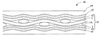
プラスチック基板20に代えて、図5に模式的に示すプラスチック基板40を用いることもできる。
Instead of the
図5に示すプラスチック基板40は、図4に示した樹脂含浸繊維3上に平坦化樹脂層42を形成した上に、無機バリア層45を形成し、さらに無機バリア層45の上に平坦化樹脂層44を形成したものである。言いかえると、図2(b)に示したプラスチック基板10の表面にさらに平坦化樹脂層を設けたものである。すなわち、平坦化樹脂層42の上に無機バリア層45を加熱条件下で堆積すると、凹凸が増大された表面しか得られないが、この上にさらに平坦化樹脂層44を形成すると、表面の凹凸が100nm以下に低減されたプラスチック基板が得られる。
A
ここで、樹脂含浸繊維布3およびこの上に形成された平坦樹脂層42とを合わせて複合体層43と呼ぶことにする。プラスチック基板40は、複合体層43上に形成された無機バリア層45と、無機バリア層45上に形成された平坦化樹脂層44とを有する。先に図4(b)に示したプラスチック基板20は、複合体層として、樹脂含浸繊維布3のみを有する構成ということになる。このように複合体層上に無機バリア層を形成し、この無機バリア層上に平坦化樹脂層を形成することによって、平坦な表面が実現される。
Here, the resin-impregnated
例えば、前述したEガラス繊維布(繊維径10μm、繊維束の幅200μm、ピッチ500μm)にエポキシ樹脂を含浸したものに平坦化樹脂層42を設けた複合体層43を用いた例を説明する。
For example, an example will be described in which a
無機バリア層45を形成する前に、約120nmの凹凸を有していた複合体層43の表面に、約200℃でSiO2を約100nm蒸着したところ、その表面の凹凸は約190nmにまで増大した。この上に、ガラス繊維布3に含浸した樹脂および平坦化樹脂層42と同じエポキシ樹脂を用いて約10μmの厚さの平坦化樹脂層44を形成した結果、表面の凹凸は約90nmまでに低減された。なお、ここで用いたプラスチック基板の大きさは127mm×127mmであり、ほぼ全面に亘り凹凸を評価した。なお、無機バリア層は少なくとも、表示領域の全面に亘って形成される必要があり、基板の全面に形成することが好ましい。ただし、液晶層や有機EL層が設けられる側の面と反対側については省略することができる。
Before the
上述したように、プラスチック基板20および40は、表面の凹凸が100nm以下に低減されているので、表示装置に適用した場合に、良好な表示を実現できる。
As described above, since the surface irregularities of the
なお、本発明の表示装置に好適に用いられるプラスチック基板を構成する材料は、上記に例に限られない。 In addition, the material which comprises the plastic substrate used suitably for the display apparatus of this invention is not restricted to the above example.
透明なプラスチック基板20および40を得るために用いられる透明樹脂としては、一般的な透明樹脂、エポキシ系樹脂、フェノール樹脂、フェノール―エポキシ系樹脂混合系、ビスマレイミド―トリアジン樹脂混合系などの熱硬化樹脂や、ポリカーボネート、ポリエーテルスルホン、ポリエーテルイミドなどの熱可塑性樹脂を使用することができる。
As the transparent resin used to obtain the transparent
また、透明繊維としては、Eガラス、Dガラス、Sガラスなどの無機繊維および芳香族ポリアミド等の樹脂などによる有機繊維を使用することができる。透明繊維は、上述したように繊維束として用いることが好ましく、織布として用いることがさらに好ましい。 Further, as the transparent fibers, inorganic fibers such as E glass, D glass, and S glass and organic fibers such as aromatic polyamide resins can be used. The transparent fiber is preferably used as a fiber bundle as described above, and more preferably used as a woven fabric.
複合基板の機械的強度を向上するため、さらに機械的特性および光学的特性の均一性を高めるために、繊維を面内に均等に配置することが好ましく、繊維径および繊維束の径は細い方が好ましく、繊維束のピッチも狭い方が良い。具体的には、個々の繊維径は、約20μm以下が好ましく、約10μm以下であることがさらに好ましい。繊維束の幅としては200μm以下であることが好ましく、繊維束のピッチは500μm以下であることが好ましい。 In order to improve the mechanical strength of the composite substrate and to further improve the uniformity of the mechanical and optical properties, it is preferable to arrange the fibers evenly in the plane, and the fiber diameter and the fiber bundle diameter are narrower It is preferable that the pitch of the fiber bundle is narrow. Specifically, the individual fiber diameter is preferably about 20 μm or less, and more preferably about 10 μm or less. The width of the fiber bundle is preferably 200 μm or less, and the pitch of the fiber bundle is preferably 500 μm or less.
また、繊維布の織り方は、上述したように、平織が最も好ましいが、朱子織および綾織等の一般的な織り方を採用することもできるし、不織布を使用することもできる。 Further, as described above, the plain weave is most preferable as the weaving method of the fiber cloth, but a general weaving method such as satin weaving and twill weaving can be adopted, and a non-woven fabric can also be used.
プラスチック基板の透明性は高い方が好ましいので、繊維と樹脂マトリクスとの界面における拡散反射や繊維による散乱を抑制するために、繊維の屈折率と樹脂マトリクスの屈折率はできるだけ一致するように選択することが好ましい。一般に、繊維の材料よりも、樹脂マトリクスの材料の方が選択の範囲が広く、また、樹脂骨格に置換基(例えばフッ素原子を導入すると低屈折率化、臭素原子を導入すると高屈折率化できる)などの方法で上記の樹脂を改質することによって屈折率を調整することが好ましい。 Since the transparency of the plastic substrate is preferably high, the refractive index of the fiber and the refractive index of the resin matrix should be matched as much as possible in order to suppress diffuse reflection at the interface between the fiber and the resin matrix and scattering by the fiber. It is preferable. In general, the resin matrix material has a wider range of selection than the fiber material, and the refractive index can be lowered by introducing substituents into the resin skeleton (for example, introducing fluorine atoms, and introducing bromine atoms). The refractive index is preferably adjusted by modifying the above resin by a method such as
プラスチック基板は、上記の繊維(繊維束または織布)および樹脂マトリクスの材料を用いて、種々の公知の方法で製造される。熱硬化性樹脂を用いる場合には、圧縮成形法、圧延成形法、注型法やトランスファー成形法などで製造することができ、熱可塑性樹脂を用いる場合は、圧縮法、射出成形法、押出し法などを用いて成形することができる。 The plastic substrate is manufactured by various known methods using the above-mentioned fibers (fiber bundle or woven fabric) and resin matrix material. When a thermosetting resin is used, it can be manufactured by a compression molding method, a rolling molding method, a casting method, a transfer molding method, or the like. When a thermoplastic resin is used, a compression method, an injection molding method, an extrusion method. It can shape | mold using etc.
図6は、本発明による実施形態の液晶表示装置200の構成を模式的に示したものである。
FIG. 6 schematically shows the configuration of the liquid
液晶表示装置200は、樹脂含浸繊維布3を含む複合体層23と複合体層23上に形成された透湿防止用の無機バリア層25と、無機バリア層25上に形成された平坦化樹脂層25とを有する繊維充填系透明プラスチック基板20と、プラスチック基板27と、プラスチック基板22とプラスチック基板27との間に設けられた液晶層26とを有する。プラスチック基板27として、透過型または透過/反射型(半透過型)の場合には、プラスチック基板20と同じ基板を用いることが好ましいが、例えば、反射型液晶表示装置を構成する場合、プラスチック基板27には透明性が要求されないので、異なる構成を採用することができる。
The liquid
プラスチック基板20およびこれと同じ構成を有するプラスチック基板27を用いて、一般的なプロセスで液晶表示装置200を作製することができる。例えば、一方の基板上に、TFT素子および透明導電膜(ITO)と配向膜を形成し、他方の基板上にカラーフィルタおよび透明導電膜(ITO)と配向膜を形成する。例えば、ITOを200℃未満の温度(例えば室温)で真空蒸着することによって透明導電膜を形成する。配向膜は、室温で塗布され、200℃未満の温度(例えば、150℃から170℃)で焼成する。カラーフィルタ側の基板にシール材を付与し、TFT側の基板にスペーサを散布した後、これらの基板を互いに貼り合せる。その後、これらの基板の間隙に真空注入法により液晶材料の注入を行う。得られた液晶表示装置の基板の表面は、上述したように、凹凸が100nm以下に低減されているので、セル厚のむらに起因する表示品位の低下は発生しない。
The liquid
図7は、本発明による実施形態の有機EL表示装置300の構成を模式的に示したものである。
FIG. 7 schematically shows a configuration of an organic
有機EL表示装置300は、樹脂含浸繊維布を含む複合体層33と複合体層33上に形成された無機バリア層35と、無機バリア層35上に形成された平坦化樹脂層34とを有する繊維充填系透明プラスチック基板30と、プラスチック30基板上に形成された陽極36と、陽極36上に形成された有機発光層37と、有機発光層37上に形成された陰極38とを有する。プラスチック基板30は、前述のプラスチック基板20と実質的に同じ構成を有しており、その表面の凹凸は100nm以下に低減されている。有機EL表示装置は、一般的なプロセスで作製することができる。例えば、平坦な表面を有する基板30上に陽極として透明電極(ITO)を形成し、真空蒸着法で有機発光層を成膜する。この有機発光層の上に陰極として透明電極(ITO)を真空蒸着によって形成すればよい。陽極(空孔注入輸送層)ならびに有機発光層、陰極(電子注入輸送層)の真空蒸着は、200℃未満の温度、例えば室温で行う。このようにして得られた有機EL装置300は、繊維充填系透明プラスチック基板30が表面平滑性に優れるため、基板表面の凹凸による表示品位のばらつきが抑制され、高い表示品位を実現される。
The organic
本発明による表示装置は、プラスチック基板を備えているので、軽量、薄型および耐衝撃性が要求される用途に好適に用いられ、従来よりも高品位の表示を提供できる。本発明は、液晶表示装置、有機EL表示装置に限られず、電気泳動型表示装置など他の表示装置にも適用できる。 Since the display device according to the present invention includes a plastic substrate, the display device is suitably used for applications requiring light weight, thinness, and impact resistance, and can provide a display with higher quality than before. The present invention is not limited to a liquid crystal display device and an organic EL display device, but can be applied to other display devices such as an electrophoretic display device.
1・・・繊維
1A・・・繊維束
1S・・・繊維布
2・・・樹脂層
3・・・樹脂含浸繊維布(複合体層)
10、20、30・・・繊維充填系透明プラスチック基板
13、23、33、43・・・樹脂含浸繊維布を含む複合体層
14、24、34、44・・・平坦化樹脂層
15、25、35、45・・・無機バリア層
16、26・・・液晶層
17、27・・・繊維充填系プラスチック基板
36・・・陽極
37・・・有機発光層
38・・・陰極
100、200・・・液晶表示装置
300・・・有機EL表示装置
DESCRIPTION OF
10, 20, 30... Fiber-filled transparent
Claims (8)
前記第1基板の前記平坦化樹脂層側に設けられた表示媒体層と、
を有する、表示装置。 A first plastic substrate having a composite layer including a fiber cloth impregnated with a resin, an inorganic barrier layer formed on the composite layer, and a planarizing resin layer formed on the inorganic barrier layer;
A display medium layer provided on the planarizing resin layer side of the first substrate;
A display device.
前記第1および第2プラスチック基板を製造するプロセスが、
樹脂が含浸された繊維布を含む複合体層を用意する工程と、
前記複合体層の表面に薄膜堆積法を用いて、第1の温度で無機バリア層を形成する工程と、
前記無機バリア層上に、前記第1の温度よりも低い第2の温度で前記平坦化樹脂層を形成する工程と、
を包含する、表示装置の製造方法。 A method for manufacturing a display device according to any one of claims 1 to 5,
A process of manufacturing the first and second plastic substrates,
Preparing a composite layer including a fiber cloth impregnated with resin;
Forming an inorganic barrier layer at a first temperature using a thin film deposition method on the surface of the composite layer;
Forming the planarizing resin layer on the inorganic barrier layer at a second temperature lower than the first temperature;
A method for manufacturing a display device, comprising:
Priority Applications (4)
| Application Number | Priority Date | Filing Date | Title |
|---|---|---|---|
| JP2003377069A JP4233433B2 (en) | 2003-11-06 | 2003-11-06 | Manufacturing method of display device |
| US10/979,724 US7378137B2 (en) | 2003-11-06 | 2004-11-02 | Display device |
| US11/859,093 US7651745B2 (en) | 2003-11-06 | 2007-09-21 | Display device |
| US12/099,196 US7923062B2 (en) | 2003-11-06 | 2008-04-08 | Display device |
Applications Claiming Priority (1)
| Application Number | Priority Date | Filing Date | Title |
|---|---|---|---|
| JP2003377069A JP4233433B2 (en) | 2003-11-06 | 2003-11-06 | Manufacturing method of display device |
Related Child Applications (1)
| Application Number | Title | Priority Date | Filing Date |
|---|---|---|---|
| JP2008293687A Division JP2009058974A (en) | 2008-11-17 | 2008-11-17 | Display device |
Publications (2)
| Publication Number | Publication Date |
|---|---|
| JP2005140976A true JP2005140976A (en) | 2005-06-02 |
| JP4233433B2 JP4233433B2 (en) | 2009-03-04 |
Family
ID=34687913
Family Applications (1)
| Application Number | Title | Priority Date | Filing Date |
|---|---|---|---|
| JP2003377069A Expired - Fee Related JP4233433B2 (en) | 2003-11-06 | 2003-11-06 | Manufacturing method of display device |
Country Status (2)
| Country | Link |
|---|---|
| US (3) | US7378137B2 (en) |
| JP (1) | JP4233433B2 (en) |
Cited By (15)
| Publication number | Priority date | Publication date | Assignee | Title |
|---|---|---|---|---|
| JP2006243393A (en) * | 2005-03-03 | 2006-09-14 | Sharp Corp | Plastic substrate for display device, and method for manufacturing the same |
| WO2008044397A1 (en) * | 2006-10-11 | 2008-04-17 | Sumitomo Bakelite Co., Ltd. | Transparent composite sheet |
| JP2008216541A (en) * | 2007-03-02 | 2008-09-18 | Sumitomo Bakelite Co Ltd | Composite material substrate with transparent electrode |
| JPWO2007144995A1 (en) * | 2006-06-15 | 2009-10-29 | シャープ株式会社 | Display device and manufacturing method thereof |
| JP2010050173A (en) * | 2008-08-20 | 2010-03-04 | Semiconductor Energy Lab Co Ltd | Light emitting device and electronic apparatus |
| JP2010182668A (en) * | 2009-01-08 | 2010-08-19 | Semiconductor Energy Lab Co Ltd | Light emitting device, and electronic device |
| JP2010191267A (en) * | 2009-02-19 | 2010-09-02 | Fuji Xerox Co Ltd | Image display medium and image display device |
| JP2012227153A (en) * | 2012-07-10 | 2012-11-15 | Semiconductor Energy Lab Co Ltd | Light emitting device and method for manufacturing light emitting device |
| US8415003B2 (en) | 2009-04-28 | 2013-04-09 | Cheil Industries Inc. | Flexible substrate for display panel and manufacturing method thereof |
| JP2014146610A (en) * | 2014-04-08 | 2014-08-14 | Semiconductor Energy Lab Co Ltd | Light-emitting device |
| WO2014148482A1 (en) * | 2013-03-19 | 2014-09-25 | 住友ベークライト株式会社 | Surface light source substrate, surface light source illumination device, and surface light source substrate manufacturing method |
| US8941011B2 (en) | 2011-08-16 | 2015-01-27 | Samsung Display Co., Ltd. | Flexible substrates and method of manufacturing the same |
| JP2016012576A (en) * | 2008-07-10 | 2016-01-21 | 株式会社半導体エネルギー研究所 | Module |
| JP2016106348A (en) * | 2013-08-02 | 2016-06-16 | 住友ベークライト株式会社 | Surface light source substrate, surface light source illumination and manufacturing method of surface light source substrate |
| JP2021082835A (en) * | 2008-04-25 | 2021-05-27 | 株式会社半導体エネルギー研究所 | Semiconductor device |
Families Citing this family (20)
| Publication number | Priority date | Publication date | Assignee | Title |
|---|---|---|---|---|
| JP4233433B2 (en) * | 2003-11-06 | 2009-03-04 | シャープ株式会社 | Manufacturing method of display device |
| JP4063225B2 (en) * | 2004-01-21 | 2008-03-19 | ソニー株式会社 | Liquid crystal display device and method of manufacturing liquid crystal display device |
| JP4378314B2 (en) * | 2005-04-26 | 2009-12-02 | シャープ株式会社 | Display device and manufacturing method of display device |
| US7678701B2 (en) * | 2006-07-31 | 2010-03-16 | Eastman Kodak Company | Flexible substrate with electronic devices formed thereon |
| JP5314013B2 (en) * | 2007-07-03 | 2013-10-16 | スリーエム イノベイティブ プロパティズ カンパニー | Backlight assembly having a transmissive optical film (OPTICAL FILM) |
| KR20090114171A (en) * | 2008-04-29 | 2009-11-03 | 삼성전자주식회사 | Display device |
| TWI475282B (en) * | 2008-07-10 | 2015-03-01 | Semiconductor Energy Lab | Liquid crystal display device and method for manufacturing the same |
| KR101560772B1 (en) | 2008-09-17 | 2015-10-16 | 삼성디스플레이 주식회사 | Display and method of fabricating the same |
| JP2010181777A (en) * | 2009-02-09 | 2010-08-19 | Hitachi Displays Ltd | Display device |
| JP2011197402A (en) * | 2010-03-19 | 2011-10-06 | Asahi Glass Co Ltd | Liquid crystal display panel, glass substrate, method for manufacturing liquid crystal display panel |
| KR101332442B1 (en) * | 2011-09-21 | 2013-11-25 | 제일모직주식회사 | Composite sheet and substrate for display device comprising the same |
| KR101887217B1 (en) * | 2012-01-06 | 2018-08-10 | 삼성디스플레이 주식회사 | Display apparatus and method of manufacturing the same |
| KR20130129675A (en) * | 2012-05-21 | 2013-11-29 | 삼성디스플레이 주식회사 | Display panel and display device including the same |
| US9701068B2 (en) | 2012-07-27 | 2017-07-11 | Apple Inc. | Transparent fiber composite |
| TWI593091B (en) * | 2012-08-20 | 2017-07-21 | 海特根微光學公司 | Fabrication of optics wafer |
| TWI488025B (en) * | 2012-08-31 | 2015-06-11 | Quanta Comp Inc | Housing of electric device and its manufacturing method |
| KR20140139299A (en) * | 2013-05-27 | 2014-12-05 | 삼성디스플레이 주식회사 | Window structure and display device having the same |
| JP6463662B2 (en) * | 2015-10-06 | 2019-02-06 | 信越化学工業株式会社 | Semiconductor encapsulating substrate encapsulating material, semiconductor encapsulating substrate encapsulating material manufacturing method, and semiconductor device manufacturing method |
| CN113327996B (en) * | 2021-05-27 | 2022-06-10 | 福斯特(嘉兴)新材料有限公司 | Transparent backboard |
| CN114038321B (en) * | 2021-11-22 | 2023-10-17 | 深圳市华星光电半导体显示技术有限公司 | Display device |
Family Cites Families (34)
| Publication number | Priority date | Publication date | Assignee | Title |
|---|---|---|---|---|
| US3789049A (en) * | 1970-12-23 | 1974-01-29 | Nitto Boseki Co Ltd | Glass fiber-reinforced epoxy resin or polyester resin composition and method for manufacturing same |
| US4917471A (en) * | 1986-08-30 | 1990-04-17 | Canon Kabushiki Kaisha | Liquid crystal device |
| EP0385475A3 (en) * | 1989-03-02 | 1991-04-03 | Asahi Glass Company Ltd. | Method of forming a transparent conductive film |
| US5689322A (en) * | 1993-07-30 | 1997-11-18 | Sharp Kabushiki Kaisha | Liquid crystal display device having regions with different twist angles |
| US5936850A (en) * | 1995-03-03 | 1999-08-10 | Canon Kabushiki Kaisha | Circuit board connection structure and method, and liquid crystal device including the connection structure |
| US5739180A (en) * | 1996-05-02 | 1998-04-14 | Lucent Technologies Inc. | Flat panel displays and methods and substrates therefor |
| US5789848A (en) * | 1996-08-02 | 1998-08-04 | Motorola, Inc. | Field emission display having a cathode reinforcement member |
| JPH112812A (en) | 1997-06-12 | 1999-01-06 | Toshiba Corp | Reflection conductive substrate, reflection liquid crystal display device, and manufacture of reflection conductive substrate |
| ATE434259T1 (en) * | 1997-10-14 | 2009-07-15 | Patterning Technologies Ltd | METHOD OF MAKING AN ELECTRICAL CAPACITOR |
| US6753047B1 (en) * | 1999-06-10 | 2004-06-22 | Ppg Industries Ohio, Inc. | Electrodes for liquid crystal cells |
| US6413645B1 (en) * | 2000-04-20 | 2002-07-02 | Battelle Memorial Institute | Ultrabarrier substrates |
| JP2001133761A (en) | 1999-11-04 | 2001-05-18 | Toshiba Corp | Liquid crystal display device and organic led device |
| JP3752949B2 (en) * | 2000-02-28 | 2006-03-08 | 日立化成工業株式会社 | Wiring substrate and semiconductor device |
| US20010038894A1 (en) * | 2000-03-14 | 2001-11-08 | Minoru Komada | Gas barrier film |
| US6492026B1 (en) * | 2000-04-20 | 2002-12-10 | Battelle Memorial Institute | Smoothing and barrier layers on high Tg substrates |
| JP2002080616A (en) | 2000-06-30 | 2002-03-19 | Sumitomo Bakelite Co Ltd | Polymer film for display element and substrate for display element using the same |
| JP2002116455A (en) | 2000-08-01 | 2002-04-19 | Kyodo Printing Co Ltd | Liquid crystal display device, electrode substrate for the same device and method of manufacturing the same device |
| US6358664B1 (en) * | 2000-09-15 | 2002-03-19 | 3M Innovative Properties Company | Electronically active primer layers for thermal patterning of materials for electronic devices |
| US20020110673A1 (en) * | 2001-02-14 | 2002-08-15 | Ramin Heydarpour | Multilayered electrode/substrate structures and display devices incorporating the same |
| SG143945A1 (en) * | 2001-02-19 | 2008-07-29 | Semiconductor Energy Lab | Light emitting device and method of manufacturing the same |
| US6590346B1 (en) * | 2001-07-16 | 2003-07-08 | Alien Technology Corporation | Double-metal background driven displays |
| US6556470B1 (en) * | 2001-07-31 | 2003-04-29 | Hewlett-Packard Company | Field addressable rewritable media |
| JP2003050384A (en) | 2001-08-07 | 2003-02-21 | Sumitomo Bakelite Co Ltd | Plastic substrate for reflective liquid crystal display element |
| JP2003048279A (en) | 2001-08-07 | 2003-02-18 | Sumitomo Bakelite Co Ltd | Method for manufacturing polymer sheet and polymer sheet manufactured by this method |
| JP2003048293A (en) | 2001-08-07 | 2003-02-18 | Sumitomo Bakelite Co Ltd | Multi-layer resin sheet |
| JP2003084264A (en) | 2001-09-11 | 2003-03-19 | Sumitomo Bakelite Co Ltd | Plastic substrate for reflective liquid crystal display element |
| JP2003098512A (en) | 2001-09-26 | 2003-04-03 | Sumitomo Bakelite Co Ltd | Plastic substrate for reflective liquid crystal display element |
| JP2003297556A (en) | 2002-04-02 | 2003-10-17 | Dainippon Printing Co Ltd | Display element substrate, display panel, display device and manufacturing method of display element substrate |
| US6890635B2 (en) * | 2002-04-26 | 2005-05-10 | E. I. Du Pont De Nemours And Company | Low loss dielectric material for printed circuit boards and integrated circuit chip packaging |
| CN100338120C (en) * | 2002-05-27 | 2007-09-19 | 日东电工株式会社 | Resin sheet and liquid-crystal cell substrate comprising the same |
| US6853478B2 (en) * | 2002-06-13 | 2005-02-08 | Hewlett-Packard Development Company, L.P. | Color display with molecular light valve |
| JP4181060B2 (en) * | 2003-02-25 | 2008-11-12 | シャープ株式会社 | Liquid crystal display |
| JP5196705B2 (en) | 2003-03-26 | 2013-05-15 | 住友ベークライト株式会社 | Optical sheet |
| JP4233433B2 (en) | 2003-11-06 | 2009-03-04 | シャープ株式会社 | Manufacturing method of display device |
-
2003
- 2003-11-06 JP JP2003377069A patent/JP4233433B2/en not_active Expired - Fee Related
-
2004
- 2004-11-02 US US10/979,724 patent/US7378137B2/en not_active Expired - Fee Related
-
2007
- 2007-09-21 US US11/859,093 patent/US7651745B2/en not_active Expired - Fee Related
-
2008
- 2008-04-08 US US12/099,196 patent/US7923062B2/en not_active Expired - Fee Related
Cited By (25)
| Publication number | Priority date | Publication date | Assignee | Title |
|---|---|---|---|---|
| JP4484733B2 (en) * | 2005-03-03 | 2010-06-16 | シャープ株式会社 | Plastic substrate for display device and manufacturing method thereof |
| JP2006243393A (en) * | 2005-03-03 | 2006-09-14 | Sharp Corp | Plastic substrate for display device, and method for manufacturing the same |
| JPWO2007144995A1 (en) * | 2006-06-15 | 2009-10-29 | シャープ株式会社 | Display device and manufacturing method thereof |
| WO2008044397A1 (en) * | 2006-10-11 | 2008-04-17 | Sumitomo Bakelite Co., Ltd. | Transparent composite sheet |
| JP2008216541A (en) * | 2007-03-02 | 2008-09-18 | Sumitomo Bakelite Co Ltd | Composite material substrate with transparent electrode |
| JP7150908B2 (en) | 2008-04-25 | 2022-10-11 | 株式会社半導体エネルギー研究所 | semiconductor equipment |
| JP2021082835A (en) * | 2008-04-25 | 2021-05-27 | 株式会社半導体エネルギー研究所 | Semiconductor device |
| US10079330B2 (en) | 2008-07-10 | 2018-09-18 | Semiconductor Energy Laboratory Co., Ltd. | Light emitting device and electronic device having an embedded pixel electrode |
| US11908976B2 (en) | 2008-07-10 | 2024-02-20 | Semiconductor Energy Laboratory Co., Ltd. | Light emitting device and electronic device |
| US11557697B2 (en) | 2008-07-10 | 2023-01-17 | Semiconductor Energy Laboratory Co., Ltd. | Flexible light emitting device comprising a polyimide resin |
| US11101407B2 (en) | 2008-07-10 | 2021-08-24 | Semiconductor Energy Laboratory Co., Ltd. | Light emitting device sealed in a fibrous body to improve manufacturability and electronic device including the light emitting device |
| US10205062B2 (en) | 2008-07-10 | 2019-02-12 | Semiconductor Energy Laboratory Co., Ltd. | Light emitting device that is highly reliable, thin and is not damaged by external local pressure and electronic device |
| JP2016012576A (en) * | 2008-07-10 | 2016-01-21 | 株式会社半導体エネルギー研究所 | Module |
| JP2010050173A (en) * | 2008-08-20 | 2010-03-04 | Semiconductor Energy Lab Co Ltd | Light emitting device and electronic apparatus |
| JP2010182668A (en) * | 2009-01-08 | 2010-08-19 | Semiconductor Energy Lab Co Ltd | Light emitting device, and electronic device |
| US9929220B2 (en) | 2009-01-08 | 2018-03-27 | Semiconductor Energy Laboratory Co., Ltd. | Light emitting device and electronic device |
| US10361258B2 (en) | 2009-01-08 | 2019-07-23 | Semiconductor Energy Laboratory Co., Ltd. | Light emitting device and electronic device |
| JP2010191267A (en) * | 2009-02-19 | 2010-09-02 | Fuji Xerox Co Ltd | Image display medium and image display device |
| US8415003B2 (en) | 2009-04-28 | 2013-04-09 | Cheil Industries Inc. | Flexible substrate for display panel and manufacturing method thereof |
| US9480165B2 (en) | 2011-08-16 | 2016-10-25 | Samsung Display Co., Ltd. | Flexible substrates and method of manufacturing the same |
| US8941011B2 (en) | 2011-08-16 | 2015-01-27 | Samsung Display Co., Ltd. | Flexible substrates and method of manufacturing the same |
| JP2012227153A (en) * | 2012-07-10 | 2012-11-15 | Semiconductor Energy Lab Co Ltd | Light emitting device and method for manufacturing light emitting device |
| WO2014148482A1 (en) * | 2013-03-19 | 2014-09-25 | 住友ベークライト株式会社 | Surface light source substrate, surface light source illumination device, and surface light source substrate manufacturing method |
| JP2016106348A (en) * | 2013-08-02 | 2016-06-16 | 住友ベークライト株式会社 | Surface light source substrate, surface light source illumination and manufacturing method of surface light source substrate |
| JP2014146610A (en) * | 2014-04-08 | 2014-08-14 | Semiconductor Energy Lab Co Ltd | Light-emitting device |
Also Published As
| Publication number | Publication date |
|---|---|
| US20080213474A1 (en) | 2008-09-04 |
| US20080013020A1 (en) | 2008-01-17 |
| US7923062B2 (en) | 2011-04-12 |
| US20050140861A1 (en) | 2005-06-30 |
| US7378137B2 (en) | 2008-05-27 |
| US7651745B2 (en) | 2010-01-26 |
| JP4233433B2 (en) | 2009-03-04 |
Similar Documents
| Publication | Publication Date | Title |
|---|---|---|
| JP4233433B2 (en) | Manufacturing method of display device | |
| US20090153961A1 (en) | Grid Polarizer and Method for Manufacturing the Same | |
| US20090073691A1 (en) | Illumination apparatus and liquid crystal display apparatus | |
| JP4181013B2 (en) | Display device and manufacturing method thereof | |
| JP4181060B2 (en) | Liquid crystal display | |
| KR20050075407A (en) | Plastic substrate and liquid crystal display having same | |
| US20210296370A1 (en) | Display device and production method thereof | |
| US20100053535A1 (en) | Display apparatus and method of fabrication the same | |
| CN108594515B (en) | Flexible polarizing cover plate, preparation method thereof, display panel comprising flexible polarizing cover plate and display device comprising flexible polarizing cover plate | |
| KR102460687B1 (en) | Flexible display device | |
| JP2001133761A (en) | Liquid crystal display device and organic led device | |
| CN109244238B (en) | Flexible substrate for display panel and manufacturing method thereof | |
| US8717529B2 (en) | Display apparatus and method of fabricating the same | |
| KR101958737B1 (en) | Flexible substrate and Method for manufacturing the same | |
| JP4484733B2 (en) | Plastic substrate for display device and manufacturing method thereof | |
| JP2009058974A (en) | Display device | |
| JP2015215388A (en) | Display device | |
| KR20100118222A (en) | A flexible substrate for display panel and a method for manufacturing the same | |
| US20100075124A1 (en) | Apparatus having planarized substrate and method of manufacturing the same | |
| KR102598479B1 (en) | Flexible substrate and flexible display device including the same | |
| JP2022143725A (en) | Laminated glass for vehicles | |
| CN114335387B (en) | Display panel and display device | |
| KR102094088B1 (en) | Composite sheet for display device, display device comprising the same and manufacturing method for the same | |
| JP2001228468A (en) | Method of manufacturing for color liquid crystal display element | |
| KR20100042083A (en) | Method of manucacturing display device |
Legal Events
| Date | Code | Title | Description |
|---|---|---|---|
| A977 | Report on retrieval |
Free format text: JAPANESE INTERMEDIATE CODE: A971007 Effective date: 20060124 |
|
| A131 | Notification of reasons for refusal |
Free format text: JAPANESE INTERMEDIATE CODE: A131 Effective date: 20070522 |
|
| A521 | Request for written amendment filed |
Free format text: JAPANESE INTERMEDIATE CODE: A523 Effective date: 20070719 |
|
| A131 | Notification of reasons for refusal |
Free format text: JAPANESE INTERMEDIATE CODE: A131 Effective date: 20080115 |
|
| A02 | Decision of refusal |
Free format text: JAPANESE INTERMEDIATE CODE: A02 Effective date: 20080610 |
|
| A521 | Request for written amendment filed |
Free format text: JAPANESE INTERMEDIATE CODE: A523 Effective date: 20080807 |
|
| A911 | Transfer to examiner for re-examination before appeal (zenchi) |
Free format text: JAPANESE INTERMEDIATE CODE: A911 Effective date: 20080815 |
|
| A131 | Notification of reasons for refusal |
Free format text: JAPANESE INTERMEDIATE CODE: A131 Effective date: 20080916 |
|
| A521 | Request for written amendment filed |
Free format text: JAPANESE INTERMEDIATE CODE: A523 Effective date: 20081117 |
|
| TRDD | Decision of grant or rejection written | ||
| A01 | Written decision to grant a patent or to grant a registration (utility model) |
Free format text: JAPANESE INTERMEDIATE CODE: A01 Effective date: 20081209 |
|
| A01 | Written decision to grant a patent or to grant a registration (utility model) |
Free format text: JAPANESE INTERMEDIATE CODE: A01 |
|
| A61 | First payment of annual fees (during grant procedure) |
Free format text: JAPANESE INTERMEDIATE CODE: A61 Effective date: 20081209 |
|
| FPAY | Renewal fee payment (event date is renewal date of database) |
Free format text: PAYMENT UNTIL: 20111219 Year of fee payment: 3 |
|
| R150 | Certificate of patent or registration of utility model |
Free format text: JAPANESE INTERMEDIATE CODE: R150 |
|
| FPAY | Renewal fee payment (event date is renewal date of database) |
Free format text: PAYMENT UNTIL: 20111219 Year of fee payment: 3 |
|
| FPAY | Renewal fee payment (event date is renewal date of database) |
Free format text: PAYMENT UNTIL: 20121219 Year of fee payment: 4 |
|
| LAPS | Cancellation because of no payment of annual fees |