JP2005128407A - Optical waveguide module - Google Patents

Optical waveguide module Download PDF

Info

Publication number
JP2005128407A
JP2005128407A JP2003366004A JP2003366004A JP2005128407A JP 2005128407 A JP2005128407 A JP 2005128407A JP 2003366004 A JP2003366004 A JP 2003366004A JP 2003366004 A JP2003366004 A JP 2003366004A JP 2005128407 A JP2005128407 A JP 2005128407A
Authority
JP
Japan
Prior art keywords
optical fiber
optical
core
optical waveguide
diameter portion
Prior art date
Legal status (The legal status is an assumption and is not a legal conclusion. Google has not performed a legal analysis and makes no representation as to the accuracy of the status listed.)
Pending
Application number
JP2003366004A
Other languages
Japanese (ja)
Inventor
Shinichiro Asari
晋一郎 浅利
Nobuyuki Asahi
信行 朝日
Current Assignee (The listed assignees may be inaccurate. Google has not performed a legal analysis and makes no representation or warranty as to the accuracy of the list.)
Panasonic Electric Works Co Ltd
Original Assignee
Matsushita Electric Works Ltd
Priority date (The priority date is an assumption and is not a legal conclusion. Google has not performed a legal analysis and makes no representation as to the accuracy of the date listed.)
Filing date
Publication date
Application filed by Matsushita Electric Works Ltd filed Critical Matsushita Electric Works Ltd
Priority to JP2003366004A priority Critical patent/JP2005128407A/en
Publication of JP2005128407A publication Critical patent/JP2005128407A/en
Pending legal-status Critical Current

Links

Images

Abstract

<P>PROBLEM TO BE SOLVED: To contrive optical coupling with a small loss between an optical fiber and an optical waveguide, and to reduce manufacturing time, in an optical waveguide module. <P>SOLUTION: The optical module 1 is structured by optically coupling an optical waveguide plate 2 and an optical fiber 3. The optical waveguide plate 2 is provided with a core 4 for light to be guided, a clad 5 which, covering the core 4, is composed of a material having a refractive index lower than that of the core 4, and an optical fiber guiding groove 6 which has a cross section in nearly the same shape as that of the core 4 and which is formed near the end face of the clad 5. The optical fiber 3 has, near the end face, a small diameter part 33 with a diameter smaller than that of other areas, and is fixed by fitting the small diameter part 33 to the optical fiber guiding groove 6 of the optical waveguide plate 2. Alignment positioning is completed in a short period of time by fitting the small diameter part 33 to the optical fiber guiding groove 6. A large difference in level is eliminated between the core 4 and the optical fiber guiding groove 6, thereby suppressing positional deviation between the core 4 and the optical fiber 3 caused by change in temperature, and realizing optical coupling with a small loss. <P>COPYRIGHT: (C)2005,JPO&NCIPI

Description

本発明は、光導波路と光ファイバとを結合した光導波路モジュールに関する。   The present invention relates to an optical waveguide module in which an optical waveguide and an optical fiber are coupled.

従来より、光情報通信システムにおいて光導波路と光ファイバとを結合した光導波路モジュールが用いられている。光導波路モジュールの製造方法の一つとして次のものが知られている(例えば、特許文献1参照)。図15に示すように、まず、シリコン基板91上に石英ガラス系のガラス膜からなる光導波路92を、光導波路92のコアの中心とシリコン基板との間隔を光ファイバの半径プラス2μm以内として形成する。次に、前記ガラス膜の一部を除去して前記シリコン基板露出面93を形成し、露出したシリコン基板露出面93の上面に光ファイバ94の外周面を接触させる。この状態で、コアの光軸方向及びこの方向に垂直でかつシリコン基板91の上面に平行な方向の2方向に光ファイバ94を移動させて光ファイバ94をコアに対して調芯し、光ファイバ94を光導波路91に紫外線硬化型接着剤95で固定する。
特開平8−36118号公報
Conventionally, an optical waveguide module in which an optical waveguide and an optical fiber are coupled is used in an optical information communication system. The following is known as one of the manufacturing methods of an optical waveguide module (for example, refer patent document 1). As shown in FIG. 15, first, an optical waveguide 92 made of a silica glass-based glass film is formed on a silicon substrate 91 such that the distance between the center of the core of the optical waveguide 92 and the silicon substrate is within the radius of the optical fiber plus 2 μm. To do. Next, a part of the glass film is removed to form the silicon substrate exposed surface 93, and the outer peripheral surface of the optical fiber 94 is brought into contact with the exposed upper surface of the silicon substrate exposed surface 93. In this state, the optical fiber 94 is moved in two directions, ie, the optical axis direction of the core and the direction perpendicular to the direction and parallel to the upper surface of the silicon substrate 91 to align the optical fiber 94 with respect to the core. 94 is fixed to the optical waveguide 91 with an ultraviolet curable adhesive 95.
JP-A-8-36118

しかしながら、上述したような光導波路モジュールの製造方法においては、時間と精度を要する光ファイバと光導波路の調芯工程が必要である。また、端面同士を突き合わせた状態で接着するので、調芯後の接着工程において接着剤の硬化収縮や温度変化等による調芯位置の変化等により、光結合損失の原因となる光軸ずれが生じる可能性がある。   However, in the method of manufacturing an optical waveguide module as described above, an alignment process of an optical fiber and an optical waveguide that requires time and accuracy is required. Also, since the end faces are bonded together, the optical axis shift that causes optical coupling loss occurs due to changes in the alignment position due to curing shrinkage of the adhesive, temperature changes, etc. in the bonding process after alignment. there is a possibility.

本発明は、上記課題を解消するものであって、短縮した製造時間で製造でき、また光ファイバと光導波路が低損失で光結合された光導波路モジュールを提供することを目的とする。   SUMMARY OF THE INVENTION An object of the present invention is to provide an optical waveguide module that solves the above-described problems and can be manufactured in a reduced manufacturing time and in which an optical fiber and an optical waveguide are optically coupled with low loss.

上記課題を達成するために、請求項1の発明は、光導波路板と光ファイバとを結合した光導波路モジュールにおいて、前記光導波路板は、光が導波するコアと、該コアを覆い該コアより低屈折率の材料よりなるクラッドと、該コアの断面と略同一形状の断面をなして該クラッドの端面付近に形成された光ファイバ案内溝とを備え、前記光ファイバは、端面付近に他の領域よりも径の小さい小径部を備え、前記光ファイバは前記光導波路板の光ファイバ案内溝に前記小径部を嵌合して固定されていることを特徴とする光導波路モジュールである。   In order to achieve the above object, the invention according to claim 1 is an optical waveguide module in which an optical waveguide plate and an optical fiber are coupled, wherein the optical waveguide plate includes a core through which light is guided, and the core covers the core. A clad made of a material having a lower refractive index, and an optical fiber guide groove formed in the vicinity of the end face of the clad and having a cross section substantially the same shape as the cross section of the core. The optical waveguide module includes a small-diameter portion having a smaller diameter than the region, and the optical fiber is fixed by fitting the small-diameter portion into an optical fiber guide groove of the optical waveguide plate.

請求項2の発明は、請求項1に記載の光導波路モジュールにおいて、光ファイバ案内溝は、光導波路板のコアの一部に平行に近接して備えられ、前記コアと光ファイバ案内溝に固定された光ファイバとが方向性結合により光学的に結合されているものである。   According to a second aspect of the present invention, in the optical waveguide module according to the first aspect, the optical fiber guide groove is provided in close proximity to a part of the core of the optical waveguide plate, and is fixed to the core and the optical fiber guide groove. The optical fiber is optically coupled by directional coupling.

請求項3の発明は、請求項2に記載の光導波路モジュールにおいて、前記光ファイバの小径部の直径が9〜50μmのものである。   According to a third aspect of the present invention, in the optical waveguide module according to the second aspect, the diameter of the small diameter portion of the optical fiber is 9 to 50 μm.

請求項4の発明は、請求項1に記載の光導波路モジュールにおいて、前記光ファイバの小径部の外形が該光ファイバの光軸中心に対して偏心しているものである。   According to a fourth aspect of the present invention, in the optical waveguide module according to the first aspect, the outer shape of the small diameter portion of the optical fiber is eccentric with respect to the optical axis center of the optical fiber.

請求項5の発明は、請求項1に記載の光導波路モジュールにおいて、前記光ファイバの小径部は、光ファイバの端面付近に短パルスレーザ光を照射することにより形成されているものである。   According to a fifth aspect of the present invention, in the optical waveguide module according to the first aspect, the small diameter portion of the optical fiber is formed by irradiating a short pulse laser beam near the end face of the optical fiber.

請求項1の発明によれば、光導波路板のコアと略同一形状で形成した光ファイバ案内溝に、光ファイバの小径部を嵌合することで調芯が精度良く完了するので、調芯位置決め時間が短縮でき、また、光導波路板のコアと光ファイバ案内溝間に大きな段差がないので、光導波路モジュールの使用状態において、温度変化によるコアと光ファイバ間の位置ずれの発生が殆どなく、光強度のカップリング損失を抑制できる。   According to the first aspect of the present invention, the alignment is completed with high accuracy by fitting the small-diameter portion of the optical fiber into the optical fiber guide groove formed in substantially the same shape as the core of the optical waveguide plate. Time can be shortened, and since there is no large step between the core of the optical waveguide plate and the optical fiber guide groove, there is almost no occurrence of displacement between the core and the optical fiber due to temperature change in the usage state of the optical waveguide module. Light intensity coupling loss can be suppressed.

請求項2の発明によれば、光ファイバ内を導波した光が、方向性結合によって光導波路板のコアに乗り移るので、光ファイバと光導波路板のコアとの断面形状の違いによる光損失がなく、カップリング損失を抑制できる。   According to the invention of claim 2, since the light guided in the optical fiber is transferred to the core of the optical waveguide plate by directional coupling, the optical loss due to the difference in cross-sectional shape between the optical fiber and the core of the optical waveguide plate is reduced. And coupling loss can be suppressed.

請求項3の発明によれば、小径部の直径が9μm以下では光信号の伝搬損失が大きく、50μm以上では方向性結合が起こりにい、という不具合のない良好な方向性結合による光結合が可能である。   According to the third aspect of the present invention, optical coupling can be achieved by good directional coupling without a problem that the propagation loss of the optical signal is large when the diameter of the small diameter portion is 9 μm or less, and directional coupling hardly occurs when the diameter is 50 μm or more. It is.

請求項4の発明によれば、光導波路板と光ファイバの結合作業時に光ファイバを光軸回りに回転して光導波路板のコアと光ファイバのコアの軸芯位置の微調整を容易に行うことができるので、光導波路板におけるコアの位置精度を緩和できる。   According to the fourth aspect of the present invention, the optical fiber is rotated around the optical axis when the optical waveguide plate and the optical fiber are joined, and fine adjustment of the axial center positions of the core of the optical waveguide plate and the core of the optical fiber is easily performed. Therefore, the position accuracy of the core in the optical waveguide plate can be relaxed.

請求項5の発明によれば、光ファイバに応力を与えることなく非接触で加工ができ、また、3次元の加工形状制御が可能である。   According to the fifth aspect of the present invention, processing can be performed without contact without applying stress to the optical fiber, and three-dimensional processing shape control is possible.

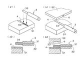
以下、本発明の一実施形態に係る光導波路モジュールについて、図面を参照して説明する。図1(a)(b)は、光導波路モジュール1と光ファイバ結合部構造を示す。光導波路モジュール1は、光導波路板2と光ファイバ3とを光結合して構成されており、光導波路板2は、光が導波するコア4と、コア4を覆いコア4より低屈折率の材料よりなるクラッド5(基板クラッド51、カバークラッド52)と、コア4の断面と略同一形状の断面をなしてクラッド5の端面付近に形成された光ファイバ案内溝6とを備え、光ファイバ3は、端面付近に他の領域よりも径の小さい小径部33を備え、光ファイバ3は光導波路板2の光ファイバ案内溝6に小径部33を嵌合して固定されている。   Hereinafter, an optical waveguide module according to an embodiment of the present invention will be described with reference to the drawings. 1A and 1B show an optical waveguide module 1 and an optical fiber coupling portion structure. The optical waveguide module 1 is configured by optically coupling an optical waveguide plate 2 and an optical fiber 3, and the optical waveguide plate 2 covers the core 4 and covers the core 4 and has a lower refractive index than the core 4. A clad 5 (substrate clad 51, cover clad 52) made of the above material, and an optical fiber guide groove 6 formed in the vicinity of the end face of the clad 5 with a cross section substantially the same shape as the cross section of the core 4. 3 includes a small-diameter portion 33 having a smaller diameter than other regions in the vicinity of the end face, and the optical fiber 3 is fixed by fitting the small-diameter portion 33 into the optical fiber guide groove 6 of the optical waveguide plate 2.

上述の光ファイバ3は、図1(b)に示すように、クラッド31と、クラッド31よりも大きな屈折率を有する中心部分のコア32とからなり、その端部には小径部33が形成されている。コア溝41の幅aは、例えばa=7μmであり、また、光ファイバ案内溝6の幅cは、例えばc=15μmである。光ファイバ小径部33とファイバ案内溝6の寸法b,c,hは互いに隙間なく、また、コア4と光ファイバ3の光軸がずれなく嵌合するように決められる。小径部33や基板クラッド51の形成、光ファイバ案内溝6等については、下記の製造工程の説明の中で述べる。   As shown in FIG. 1B, the above-described optical fiber 3 includes a clad 31 and a core 32 at a central portion having a refractive index larger than that of the clad 31, and a small-diameter portion 33 is formed at an end thereof. ing. The width a of the core groove 41 is, for example, a = 7 μm, and the width c of the optical fiber guide groove 6 is, for example, c = 15 μm. The dimensions b, c, and h of the optical fiber small-diameter portion 33 and the fiber guide groove 6 are determined so that there is no gap between them and the optical axes of the core 4 and the optical fiber 3 are fitted with no deviation. The formation of the small-diameter portion 33 and the substrate cladding 51, the optical fiber guide groove 6 and the like will be described in the description of the manufacturing process below.

光導波路モジュール1の製造工程を説明する。図2は、光ファイバ3の小径部33の形成方法を示し、図3は、光導波路モジュール1の製造工程を示す。[光ファイバ小径部形成工程]光ファイバ3の小径部33は、図2(a)に示すように、石英系の光ファイバ3の端部をフッ酸溶液7に浸してエッチングによりクラッド31の一部を除去し、光ファイバ3の端面付近のファイバ径を小さくして形成される。クラッド31の一部を除去した領域(クラッド除去部)のファイバ径は、シングルモード光ファイバの場合ではφ9〜50μm程度とする。エッチングする領域の制御は、例えば、除去する部分以外をフッ酸に浸漬しないか、又は除去部以外のクラッド31表面をNi−Cr−Mo合金などでメタライズして保護することによって行うことができる。フッ酸濃度50%では、エッチング速度0.6μm/分であったので、125μmφの光ファイバをφ30μmにエッチングするのに、80分程度要するが、この方法を用いると一度に大量の光ファイバの加工が可能である。   A manufacturing process of the optical waveguide module 1 will be described. FIG. 2 shows a method of forming the small diameter portion 33 of the optical fiber 3, and FIG. 3 shows a manufacturing process of the optical waveguide module 1. [Optical Fiber Small Diameter Forming Step] As shown in FIG. 2A, the small diameter section 33 of the optical fiber 3 is formed by immersing the end of the quartz-based optical fiber 3 in the hydrofluoric acid solution 7 and etching it. This is formed by removing the portion and reducing the fiber diameter in the vicinity of the end face of the optical fiber 3. In the case of a single mode optical fiber, the fiber diameter of the region from which a part of the cladding 31 is removed (cladding removal portion) is about 9 to 50 μm. The region to be etched can be controlled, for example, by not immersing the portion other than the portion to be removed in hydrofluoric acid, or by protecting the surface of the clad 31 other than the removed portion with a Ni—Cr—Mo alloy or the like. When the concentration of hydrofluoric acid is 50%, the etching rate is 0.6 μm / min. Therefore, it takes about 80 minutes to etch an optical fiber of 125 μmφ to 30 μm. Is possible.

[基板クラッド形成工程]基板クラッド51は、コア溝及び光ファイバ案内溝となるべき部分に凸部を備えた金型を用いて、プレス成形や射出成形を行い、一度の成形処理によって、図3(a)に示すように、コア溝41及び光ファイバ案内溝6を表面に備えて形成される。ここで用いる金型は、LIGA(Lithography Galvanoformung Abformung)工法等を用いて製造することができる。LIGA工法は、フォトエレクトロプレーティングのやり方で、立体的に奥行きが出るようにしたプロセスである。例えば、フォトレジストを深く立体的に彫った後で、電気めっき(電気鋳造)して金型を作ることができる。   [Substrate Clad Forming Step] The substrate clad 51 is press-molded or injection-molded using a mold having convex portions at the portions to be the core groove and the optical fiber guide groove. As shown to (a), the core groove 41 and the optical fiber guide groove 6 are provided in the surface, and it forms. The mold used here can be manufactured using a LIGA (Lithography Galvanoformung Abformung) method or the like. The LIGA method is a process in which a three-dimensional depth is obtained by a photoelectroplating method. For example, after a photoresist is deeply three-dimensionally carved, a metal mold can be made by electroplating (electrocasting).

コア溝41の断面形状は方形であり、前出の図1(b)に示す幅aは、シングルモード対応の場合、5〜20μmである。また、光ファイバ案内溝6の形状、すなわち、前出の図1(b)に示す溝の幅c、溝の高さh、及び溝の長さbは、光ファイバ3の小径部33が嵌合される寸法に合わせて形成される。寸法の代表例を示すと、コア溝41の幅a=7μm、光ファイバ案内溝6の幅c=15μmである。   The cross-sectional shape of the core groove 41 is a square, and the width a shown in FIG. 1B is 5 to 20 μm in the case of the single mode. Further, the shape of the optical fiber guide groove 6, that is, the groove width c, the groove height h, and the groove length b shown in FIG. It is formed according to the dimensions to be combined. As representative examples of dimensions, the width a of the core groove 41 is 7 μm, and the width c of the optical fiber guide groove 6 is 15 μm.

基板クラッド51に用いる樹脂として、光透過率の高いPMMA、エポキシ樹脂、アクリル樹脂、フッ素系樹脂等を用いることができる。実施例では、例えば、PMMAの場合、光の屈折率nが1.492のものが用いられる。   As the resin used for the substrate clad 51, PMMA, epoxy resin, acrylic resin, fluorine resin, or the like having high light transmittance can be used. In the embodiment, for example, in the case of PMMA, a light having a refractive index n of 1.492 is used.

[光ファイバ配置工程]続く工程で、上述の基板クラッド51の光ファイバ案内溝6に光ファイバ3が嵌合、配置される。このとき、光ファイバ案内溝6の形状は、光ファイバ3の小径部33形状とほぼ同等か0.5〜1μm程度大きく形成すると嵌合時に、光ファイバ端部の破損を避けることができる。   [Optical Fiber Arrangement Step] In the subsequent step, the optical fiber 3 is fitted and arranged in the optical fiber guide groove 6 of the substrate clad 51 described above. At this time, if the shape of the optical fiber guide groove 6 is substantially the same as the shape of the small-diameter portion 33 of the optical fiber 3 or about 0.5 to 1 μm larger, damage to the end portion of the optical fiber can be avoided during fitting.

[接着剤塗布工程]図3(b)に示すように、ディスペンサ42を用いて、光ファイバ3のコア32と同等の屈折率(n=1.497)を有する接着剤43を、光ファイバ案内溝6に嵌合された光ファイバ小径部33周辺に塗布する。このとき、コア溝41に接着剤43を充填して光導波路(コア4)の形成と光ファイバの接着とを同時に行うことができる。   [Adhesive Application Step] As shown in FIG. 3B, an adhesive 43 having a refractive index (n = 1.497) equivalent to that of the core 32 of the optical fiber 3 is replaced with an optical fiber guide by using a dispenser 42. It is applied to the periphery of the optical fiber small-diameter portion 33 fitted in the groove 6. At this time, the core groove 41 can be filled with the adhesive 43 to simultaneously form the optical waveguide (core 4) and bond the optical fiber.

導波路コア4を形成する樹脂と光ファイバ接着に用いる樹脂との屈折率が異なる樹脂を用いる場合、コア溝41に、例えば屈折率n=1.497の樹脂を充填し、その後、光ファイバ案内溝6に、基板クラッド51と同じ屈折率n=1.492を有する樹脂を塗布する。すなわち、光が導波するコアの屈折率を高くし、接着剤に低屈折率接着剤を用いて、光伝搬への悪影響がないようにする。例えば、使用する接着剤の屈折率が光ファイバのコアの屈折率より0.001〜0.05ほど低いものを用いることで、接着剤が光ファイバのクラッド領域と同じ効果を持つ。これによって、光ファイバの小径部から光信号が漏れることを防ぎ、高効率で光信号を転送できる。   When using a resin having a different refractive index between the resin forming the waveguide core 4 and the resin used for bonding the optical fiber, the core groove 41 is filled with, for example, a resin having a refractive index n = 1.497, and then the optical fiber guide. A resin having the same refractive index n = 1.492 as that of the substrate cladding 51 is applied to the groove 6. That is, the refractive index of the core through which light is guided is increased, and a low refractive index adhesive is used as an adhesive so as not to adversely affect light propagation. For example, the adhesive has the same effect as that of the cladding region of the optical fiber by using an adhesive having a refractive index lower by 0.001 to 0.05 than the refractive index of the core of the optical fiber. As a result, the optical signal can be prevented from leaking from the small diameter portion of the optical fiber, and the optical signal can be transferred with high efficiency.

[カバークラッド接合工程]上述の樹脂充填、接着剤塗布を行った基板クラッドの上に、図3(c)に示すように、厚さ100μm程度のカバークラッド52を配置して、上面よりプレスする。プレスによってコア形成用の樹脂液がカバークラッド52と基板クラッド51間の全面に行き渡る。その後、カバークラッド52の上部から光照射することにより、コア樹脂と接着剤を硬化させる。これにより、基板クラッド51、カバークラッド52、光ファイバ3が接合され、コアが形成されて、光導波路モジュール1が完成する。   [Cover Cladding Step] As shown in FIG. 3C, a cover clad 52 having a thickness of about 100 μm is disposed on the substrate clad subjected to the above resin filling and adhesive application and pressed from above. . The resin liquid for core formation spreads over the entire surface between the cover clad 52 and the substrate clad 51 by pressing. Thereafter, the core resin and the adhesive are cured by irradiating light from the upper part of the cover clad 52. As a result, the substrate clad 51, the cover clad 52, and the optical fiber 3 are joined to form a core, and the optical waveguide module 1 is completed.

カバークラッド52に用いる樹脂として、上述した基板クラッド51に用いる樹脂と同様の樹脂を用いることができ、本実施例ではPMMAで屈折率n=1.492のものを用いた。   As the resin used for the cover clad 52, a resin similar to the resin used for the substrate clad 51 described above can be used. In this embodiment, a resin having a refractive index n = 1.492 is used.

上述のように、光導波路モジュール1は、図1と図3で示したように、光導波路板2のコア4と略同一形状で形成した光ファイバ案内溝6に、光ファイバ3の小径部33を嵌合することで、コア4と光ファイバ3の光軸を一致させる調芯が完了するので、調芯位置決め時間が短縮できる。また、光導波路板2のコア4と光ファイバ案内溝6との間に大きな段差がないので、温度変化によるコア4と光ファイバ3間の位置ずれの発生が殆どなく、温度変化による光強度のカップリング損失が抑制された低損失光結合が実現され、光導波路モジュール1の安定した使用状態が実現される。   As described above, the optical waveguide module 1 includes the small-diameter portion 33 of the optical fiber 3 in the optical fiber guide groove 6 formed in substantially the same shape as the core 4 of the optical waveguide plate 2 as shown in FIGS. Since the alignment for matching the optical axes of the core 4 and the optical fiber 3 is completed, the alignment positioning time can be shortened. Further, since there is no large step between the core 4 of the optical waveguide plate 2 and the optical fiber guide groove 6, there is almost no displacement between the core 4 and the optical fiber 3 due to temperature change, and the light intensity due to temperature change is reduced. Low-loss optical coupling with reduced coupling loss is realized, and a stable use state of the optical waveguide module 1 is realized.

次に、本発明の他の一実施形態に係る光導波路モジュールについて説明する。図4は光導波路モジュール1を示し、図5(a)〜(d)はその製造工程を示す。この光導波路モジュール1の光ファイバ案内溝6は、図4(a)(b)に示すように、光導波路板2のコア4の一部(端部)に平行に近接して備えられ、コア4と光ファイバ案内溝6に固定された光ファイバ3(の小径部)とが方向性結合により光学的に結合されたものである。   Next, an optical waveguide module according to another embodiment of the present invention will be described. 4 shows the optical waveguide module 1, and FIGS. 5A to 5D show the manufacturing process thereof. As shown in FIGS. 4A and 4B, the optical fiber guide groove 6 of the optical waveguide module 1 is provided in parallel and close to a part (end portion) of the core 4 of the optical waveguide plate 2. 4 and the optical fiber 3 (the small diameter portion thereof) fixed to the optical fiber guide groove 6 are optically coupled by directional coupling.

このような方向性結合を用いる光導波路モジュール1において、光ファイバ3の小径部33の直径が9〜50μmのものが用いられる。小径部33の直径が9μm以下では光信号が伝達できず、また、50μm以上では方向性結合が起こりにいからである。また、光ファイバ3の小径部33の直径を9〜20μm程度にすると、方向性結合現象がさらに誘発されやすくなり、結合性がより改善される。   In the optical waveguide module 1 using such directional coupling, the one having a diameter of the small diameter portion 33 of the optical fiber 3 of 9 to 50 μm is used. This is because if the diameter of the small diameter portion 33 is 9 μm or less, an optical signal cannot be transmitted, and if it is 50 μm or more, directional coupling is unlikely to occur. Further, when the diameter of the small diameter portion 33 of the optical fiber 3 is about 9 to 20 μm, the directional coupling phenomenon is further easily induced, and the coupling property is further improved.

また、コア溝41と光ファイバ案内溝6の中心間距離e、及び平行に走っている部分の長さ(移行距離)dには、中心間距離eが近いほど短い移行距離dで、互いに光が乗り移る(方向性結合する)ことができるという関係がある。例えば、断面形状が□6μmのコア溝41に対して、a=8μmのときd=0.95mmで、またa=10μmのときd=1mmで光ファイバから導波路(コア4)に光が乗り移った。   Further, the distance e between the centers of the core groove 41 and the optical fiber guide groove 6 and the length (transition distance) d of the portion running in parallel with each other have a shorter transition distance d as the distance e between the centers is shorter. Can be transferred (directly coupled). For example, light is transferred from the optical fiber to the waveguide (core 4) with respect to the core groove 41 having a cross-sectional shape of □ 6 μm when d = 0.95 mm when a = 8 μm and d = 1 mm when a = 10 μm. It was.

このように光ファイバ3をコア4に近接して配置することにより、光導波路(コア4)と、光ファイバ3との間で方向性結合による光信号の伝達が行われるため、従来例にあるような調芯工程が不要となる。また、光ファイバ内を導波した光が、方向性結合によって光導波路板のコアに乗り移るので、光ファイバと光導波路板のコアとの断面形状の違いによる光損失がなく、カップリング損失を抑制できる。基板クラッド51は、リソグラフィを用いた露光・現像による方法や、前述したような金型を用いる方法により、容易に形成できる。以下に製造工程を述べる。   By arranging the optical fiber 3 in the vicinity of the core 4 in this way, an optical signal is transmitted by directional coupling between the optical waveguide (core 4) and the optical fiber 3, which is the conventional example. Such an alignment process becomes unnecessary. In addition, since the light guided in the optical fiber is transferred to the core of the optical waveguide plate by directional coupling, there is no optical loss due to the difference in cross-sectional shape between the optical fiber and the core of the optical waveguide plate, and the coupling loss is suppressed. it can. The substrate clad 51 can be easily formed by a method using exposure / development using lithography or a method using a mold as described above. The manufacturing process will be described below.

[光ファイバ小径部/基板クラッド形成工程]光ファイバ3の小径部33の形成は、前述の光ファイバ小径部形成工程と同様に行われる。光ファイバ小径部33の径は、シングルモード光ファイバの場合、φ9〜50μm程度とされる。基板クラッド51の形成も、前述同様に行われる。また、コア溝41の断面形状は、シングルモード対応の場合は□5〜20μmとされる。光ファイバ取付構造の形状(溝の幅・高さ)は、光ファイバの小径部33が嵌合されるように形成する。   [Optical Fiber Small Diameter Portion / Substrate Cladding Forming Step] The small diameter portion 33 of the optical fiber 3 is formed in the same manner as the optical fiber small diameter portion forming step. In the case of a single mode optical fiber, the diameter of the optical fiber small diameter portion 33 is about φ9 to 50 μm. The formation of the substrate cladding 51 is performed in the same manner as described above. Further, the cross-sectional shape of the core groove 41 is set to □ 5 to 20 μm in the case of the single mode. The shape (width / height of the groove) of the optical fiber mounting structure is formed so that the small diameter portion 33 of the optical fiber is fitted.

[コア形成工程]図5(a)に示すように、ディスペンサ42を用いて、コア溝41にコア溝41から樹脂43液が少し溢れる程度に、メタクリレート系樹脂(屈折率1.497)を充填する。また、図示のように、コア溝41の全周を基板クラッド51で囲む構造とすることで、樹脂43を端面でせき止めることができ、基板クラッド端面から樹脂液が溢れ出すことがなく、後工程の光ファイバ配置工程において光ファイバに上記樹脂液が付着することを防止できる。従って、このコア溝41構造により、光ファイバ3の位置決め精度確保や樹脂液付着による不具合防止ができる。   [Core Forming Step] As shown in FIG. 5A, using a dispenser 42, the core groove 41 is filled with a methacrylate resin (refractive index 1.497) so that the resin 43 liquid slightly overflows from the core groove 41. To do. Further, as shown in the drawing, the entire periphery of the core groove 41 is surrounded by the substrate clad 51, so that the resin 43 can be damped by the end surface, and the resin liquid does not overflow from the end surface of the substrate clad, so that a post process is performed. In the optical fiber arranging step, it is possible to prevent the resin liquid from adhering to the optical fiber. Therefore, with this core groove 41 structure, it is possible to ensure the positioning accuracy of the optical fiber 3 and prevent problems due to resin liquid adhesion.

[光ファイバ配置工程]図5(b)に示すように、光ファイバ3を基板クラッド51の光ファイバ案内溝に嵌合配置する。   [Optical Fiber Arrangement Step] As shown in FIG. 5B, the optical fiber 3 is fitted and arranged in the optical fiber guide groove of the substrate clad 51.

[接着剤塗布工程]図5(c)に示すように、ディスペンサ44を用いて、基板クラッド51と同じ屈折率n=1.492を有する光硬化型アクリレート系接着剤45を、光ファイバ小径部に塗布する。このあと、前述同様に、カバークラッド接合工程を行い光導波路モジュール1が完成する。   [Adhesive Application Step] As shown in FIG. 5 (c), using a dispenser 44, a photocurable acrylate adhesive 45 having the same refractive index n = 1.492 as that of the substrate clad 51 is applied to the optical fiber small diameter portion. Apply to. Thereafter, as described above, a cover clad bonding process is performed to complete the optical waveguide module 1.

次に、上述と同じ方向性結合を用いた他の光導波路モジュールについて説明する。図6は光導波路モジュールの方向性結合部の構造を示す。図6(a1)(a2)に示すように、基板クラッド51には、上述のような光ファイバ案内溝は設けられていない。光ファイバ3は、基板クラッド51に形成されたコア4の上の領域60に直接、コア4に平行に配置される。そして、図6(b1)(b2)に示すように、光ファイバ案内溝6を有するカバークラッド52を上からかぶせて、光導波路モジュールが形成される。   Next, another optical waveguide module using the same directional coupling as described above will be described. FIG. 6 shows the structure of the directional coupling portion of the optical waveguide module. As shown in FIGS. 6A1 and 6A2, the substrate clad 51 is not provided with the above-described optical fiber guide groove. The optical fiber 3 is disposed in parallel to the core 4 directly in the region 60 on the core 4 formed in the substrate cladding 51. Then, as shown in FIGS. 6 (b1) and 6 (b2), an optical waveguide module is formed by covering the cover clad 52 having the optical fiber guide groove 6 from above.

なお、光ファイバ案内溝6を有するカバークラッド52を用いることなく、型を用いたり、塗布を行うことにより、基板クラッドの上に直接、カバークラッドを形成することもできる。このように、光ファイバ案内溝を基板クラッドから無くし、光ファイバの小径部を光導波路板のコア部の上部に直接配置することで、上記同様に方向性結合現象による光信号の伝達が可能である。   Note that the cover clad can be formed directly on the substrate clad by using a mold or coating without using the cover clad 52 having the optical fiber guide groove 6. In this way, by eliminating the optical fiber guide groove from the substrate clad and arranging the small diameter portion of the optical fiber directly above the core portion of the optical waveguide plate, the optical signal can be transmitted by the directional coupling phenomenon as described above. is there.

次に、本発明のさらに他の一実施形態に係る光導波路モジュールについて説明する。図7は光導波路モジュール製造時の調芯方法を示す。この光導波路モジュールに用いる光ファイバの小径部33は、図7(b)(c)に示すように、その外形が光ファイバ3の光軸中心、すなわちコア31の中心に対して偏心している。偏心した小径部33を有する光ファイバをの形成については後述する。   Next, an optical waveguide module according to still another embodiment of the present invention will be described. FIG. 7 shows an alignment method when manufacturing the optical waveguide module. As shown in FIGS. 7B and 7C, the outer diameter of the small-diameter portion 33 of the optical fiber used in this optical waveguide module is eccentric with respect to the optical axis center of the optical fiber 3, that is, the center of the core 31. The formation of the optical fiber having the eccentric small diameter portion 33 will be described later.

この偏心した小径部を有する光ファイバ3を用いて、前出の図3で示した工程と同様に工程をすすめて、図7(a)に示すように、カバークラッド51をのせてプレスした後、調芯のための微調整が行われる。図の左方の光ファイバ3に光L0を入射し、図の右方の光ファイバ3から出射される光L1,L2の強度を測定しながら、カバークラッドの上面より接着剤を硬化させる光を照射する。このとき、光ファイバ3をそれぞれの軸回りに回転させて、出射光の強度が最も大きいところで回転を止め、その状態で接着剤を完全に硬化させる。光導波路板と光ファイバの結合作業時に軸芯位置の微調整を容易に行うことができるので、光導波路板におけるコアの位置精度を緩和できる。   After the optical fiber 3 having the eccentric small-diameter portion is used, the same process as that shown in FIG. 3 is performed, and the cover clad 51 is placed and pressed as shown in FIG. 7A. Fine adjustment for alignment is performed. The light L0 is incident on the left optical fiber 3 in the figure, and the intensity of the light L1 and L2 emitted from the right optical fiber 3 in the figure is measured, and the light that hardens the adhesive from the upper surface of the cover clad. Irradiate. At this time, the optical fiber 3 is rotated about each axis, and the rotation is stopped at the point where the intensity of the emitted light is the highest, and the adhesive is completely cured in this state. Since the fine adjustment of the axial center position can be easily performed at the time of coupling the optical waveguide plate and the optical fiber, the position accuracy of the core in the optical waveguide plate can be relaxed.

次に、光ファイバの小径部33をレーザ光により形成する方法を、図8により、説明する。光ファイバ3のコア部を整形する場合、切削や研削等の機械加工による方法によると、石英ファイバの場合、脆性材料であるため、ファイバが破断することがある。そこで、レーザ光により非接触で加工を行うと、加工時の応力負荷を抑制できる。レーザ光としては、熱応力が負荷されないように、短パルスレーザ光が望ましく、例えば、パルス幅1〜200nsecのレーザ光を用いることができる。パルス幅がnsオーダ以下のps、fsのレーザでも同様の効果が得られるが、短パルスになるほど1パルス当りの除去量が低下するので生産性が低下する。   Next, a method of forming the small-diameter portion 33 of the optical fiber with laser light will be described with reference to FIG. When the core portion of the optical fiber 3 is shaped, according to a method by machining such as cutting or grinding, the fiber may break because the quartz fiber is a brittle material. Therefore, when non-contact processing is performed with laser light, stress load during processing can be suppressed. The laser beam is preferably a short pulse laser beam so that thermal stress is not applied. For example, a laser beam having a pulse width of 1 to 200 nsec can be used. A similar effect can be obtained with a ps and fs laser having a pulse width of ns order or less. However, the shorter the pulse, the lower the removal amount per pulse, and the lower the productivity.

また、石英ファイバの場合、可視や赤外領域の光に対して、透明性を有しているので、レーザ光の吸収効率が問題になることもある。これらのことを考慮して、例えば、エキシマレーザを用いて加工を行った。ArF(アルゴンフッ素)レーザ光の波長は、石英に対して吸収があるので、これを用いることとし、図8に示すように、レーザ光源8からのレーザ光LBを、ミラー81及び集光レンズ82を介して、エネルギー密度1.0J/cm〜5J/cmとして、ファイバ3に照射した。エキシマレーザは、パルスレーザであるので、パルス数で、小径部33におけるクラッド除去量を制御できる。レーザ光の照射サイズは、遮蔽マスクを用いて、1〜100μmφに整形した。レーザ光LBを走査するとともに、光ファイバ3をその軸回りに回転することにより、ファイバ小径部33の形状を所望の形状に整形できる。例えば、前述の偏心した小径部33を有する光ファイバを、図8に示す方法で形成できる。 In addition, in the case of a quartz fiber, since it has transparency with respect to light in the visible or infrared region, the absorption efficiency of laser light may become a problem. Considering these matters, for example, processing was performed using an excimer laser. Since the wavelength of ArF (argon fluorine) laser light is absorbed by quartz, this is used, and the laser light LB from the laser light source 8 is converted into a mirror 81 and a condenser lens 82 as shown in FIG. through, as the energy density of 1.0J / cm 2 ~5J / cm 2 , it was irradiated to the fiber 3. Since the excimer laser is a pulse laser, the amount of clad removal in the small diameter portion 33 can be controlled by the number of pulses. The irradiation size of the laser beam was shaped to 1 to 100 μmφ using a shielding mask. By scanning the laser beam LB and rotating the optical fiber 3 about its axis, the shape of the small fiber diameter portion 33 can be shaped into a desired shape. For example, an optical fiber having the above-mentioned eccentric small diameter portion 33 can be formed by the method shown in FIG.

次に、本発明のさらに他の一実施形態に係る光導波路モジュールについて説明する。図9は、光ファイバの先端部とその嵌合状態を示し、図10は、さらに他の形状の光ファイバの先端部とその嵌合状態を示す。これらの嵌合状態を有する光導波路モジュールは、狙い形状に形成されたファイバ先端部を有する光ファイバに対し、光導波路板の導波路部にファイバ先端形状にあった形状を形成して、光ファイバを光導波路板に結合する際に、接続信頼性を向上させるものである。図9(a)(b)に示すように、光ファイバ3の先端部分の領域3A,3B,3Cのうち、途中の領域3Bの部分のコア31がむき出しされ、小径部が形成されている。また、その先端形状に合った形状が、図9(c)に示すように基板クラッド51のコア溝41端部に、光ファイバ案内溝6A,6B,6Cとして形成されている。そして、図9(d)に示すように、光ファイバ3の領域3A,3B,3Cとファイバ案内溝6A,6B,6Cのそれぞれを嵌合させて、光導波路モジュールが形成される。図10に示す光ファイバ3は、その先端の小径部33をテーパ形状とし、また、光ファイバ案内溝6の形状が、対応する形状とされている。これらの光ファイバ案内溝及びコア溝41の形成は、例えば、光ファイバ案内溝及びコア溝41の両方の対応するパターンを有するマスクを用いて、フォトリソグラフイにより行うことができる。   Next, an optical waveguide module according to still another embodiment of the present invention will be described. FIG. 9 shows the tip of an optical fiber and its fitted state, and FIG. 10 shows the tip of an optical fiber of another shape and its fitted state. The optical waveguide module having these fitting states is obtained by forming a shape corresponding to the fiber tip shape in the waveguide portion of the optical waveguide plate with respect to the optical fiber having the fiber tip portion formed in the target shape. When connecting to the optical waveguide plate, the connection reliability is improved. As shown in FIGS. 9A and 9B, the core 31 in the region 3B in the middle of the regions 3A, 3B, 3C at the tip of the optical fiber 3 is exposed to form a small diameter portion. Further, shapes corresponding to the tip shape are formed as optical fiber guide grooves 6A, 6B, 6C at the end of the core groove 41 of the substrate clad 51 as shown in FIG. 9C. Then, as shown in FIG. 9D, the optical waveguide module is formed by fitting the regions 3A, 3B, 3C of the optical fiber 3 and the fiber guide grooves 6A, 6B, 6C, respectively. In the optical fiber 3 shown in FIG. 10, the small-diameter portion 33 at the tip thereof is tapered, and the shape of the optical fiber guide groove 6 is a corresponding shape. The optical fiber guide groove and the core groove 41 can be formed by photolithography using a mask having a pattern corresponding to both the optical fiber guide groove and the core groove 41, for example.

上述の図9と図10に示した先端部を有する光ファイバの製造方法を、図11、図12により説明する。図11(a)に示すように、光ファイバ3の先端部の2箇所にマスクM1,M2を施して、エッチング液7に浸漬することにより、小径部3Bにコアが露出した光ファイバが得られる。また、図11(b)に示すように、光ファイバ3の先端から離れたところにマスクM3を施して、エッチング液7に浸漬することにより、先端部がテーパ形状となった小径部を有する光ファイバが得られる。   A method for manufacturing the optical fiber having the tip shown in FIGS. 9 and 10 will be described with reference to FIGS. As shown in FIG. 11 (a), masks M1 and M2 are applied to two locations at the tip of the optical fiber 3 and immersed in an etching solution 7, whereby an optical fiber having a core exposed at the small diameter portion 3B is obtained. . Further, as shown in FIG. 11 (b), a mask M3 is provided at a position away from the tip of the optical fiber 3 and immersed in the etching solution 7, so that the tip has a small diameter portion with a tapered shape. A fiber is obtained.

エッチングの詳細説明をする。エッチング液7として、例えば、フッ酸溶液を用いる場合、エッング速度が比較的遅く、光ファイバのクラッドの溶解量の制御が容易である。また、エッチング速度は、フッ酸濃度を変化させて制御することが可能である。マスクM1〜M3の形成は、光ファイバ先端外形部にAuのコーティング膜をスバッタ法により形成される。また、コーティング膜は、Ni−Cr−Mo合金によるメタライズで形成してもよい。フッ酸溶液を用いてエッチングする場合、コーティング膜としてフッ素樹脂膜を用いてもよい。   The etching will be described in detail. For example, when a hydrofluoric acid solution is used as the etching solution 7, the etching rate is relatively slow, and the dissolution amount of the clad of the optical fiber can be easily controlled. The etching rate can be controlled by changing the hydrofluoric acid concentration. The masks M1 to M3 are formed by forming a coating film of Au on the outer end portion of the optical fiber by a sputtering method. The coating film may be formed by metallization using a Ni—Cr—Mo alloy. In the case of etching using a hydrofluoric acid solution, a fluororesin film may be used as the coating film.

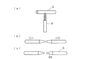
また、先端がテーパ形状となった小径部を有する光ファイバは、図12(a)〜(c)に示すように、光ファイバ3に引張応力を付加しながらバーナ9により加熱して切断することにより得られる。石英ファイバの場合、1600℃〜2000℃に加熱しファイバ外径の最小値が、20μmφになるところで、光ファイバを切断すると光ファイバ端部がテーパ形状になり、所望の形状が得られる。この形状は、光ファイバを加熱する領域、引張応力、及び歪速度により制御可能である。光ファイバの加熱は、酸水素バーナや炭酸ガスレーザ等の赤外線レーザによって局所加熱が可能であり、これらを用いて所望のテーパ形状を形成可能である。   Also, the optical fiber having a small diameter portion with a tapered tip is heated and cut by the burner 9 while applying tensile stress to the optical fiber 3 as shown in FIGS. 12 (a) to 12 (c). Is obtained. In the case of quartz fiber, when the optical fiber is cut at a temperature of 1600 ° C. to 2000 ° C. and the minimum value of the fiber outer diameter becomes 20 μmφ, the end of the optical fiber becomes a tapered shape, and a desired shape is obtained. This shape can be controlled by the region in which the optical fiber is heated, the tensile stress, and the strain rate. The optical fiber can be heated locally by an infrared laser such as an oxyhydrogen burner or a carbon dioxide laser, and a desired taper shape can be formed using these.

次に、本発明のさらに他の一実施形態に係る光導波路モジュールについて説明する。図13は、光ファイバの先端部とその嵌合状態を示し、図10は、さらに他の嵌合状態を示す。前出の図3(a)(b)に関して説明した光ファイバ配置工程では、光ファイバ案内溝の寸法を光ファイバの外径より0.5〜1μm程度大きく形成して嵌合時の光ファイバ破損を避けることを述べたが、ポリマ導波路の場合、光ファイバ案内溝の寸法を小さくして、光ファイバを破損することなく、精度良く位置決めをすることができる。すなわち、光導波路(コア及びクラッド)が、ポリマ等のように、ファイバ材質より硬度が低い材料の場合、光ファイバ案内溝に光ファイバを位置合わせする際に、図13(a)(b)に示すように、光ファイバ小径部33の外径d1よりも光ファイバ案内溝6の溝幅d2を小さくする。このような寸法関係のもとで、光ファイバ小径部33を光ファイバ案内溝6に嵌合させると、図13(c)に示すように、光ファイバ案内溝の側壁が変形するとともに、側壁から光ファイバ小径部33をクランプする力Fが発生する。力Fによって、光ファイバ小径部33が光ファイバ案内溝の中心に精度良く配置・保持され、また、その後の接着等の製造工程においても位置ずれの発生も抑制される。   Next, an optical waveguide module according to still another embodiment of the present invention will be described. FIG. 13 shows the tip of the optical fiber and its fitted state, and FIG. 10 shows yet another fitted state. In the optical fiber placement step described with reference to FIGS. 3A and 3B, the optical fiber guide groove is formed to have a size larger than the outer diameter of the optical fiber by about 0.5 to 1 μm, and the optical fiber is broken when fitted. However, in the case of a polymer waveguide, it is possible to reduce the size of the optical fiber guide groove and perform positioning accurately without damaging the optical fiber. That is, when the optical waveguide (core and clad) is made of a material whose hardness is lower than that of the fiber material such as a polymer or the like, when aligning the optical fiber with the optical fiber guide groove, FIGS. As shown, the groove width d2 of the optical fiber guide groove 6 is made smaller than the outer diameter d1 of the optical fiber small diameter portion 33. When the optical fiber small-diameter portion 33 is fitted into the optical fiber guide groove 6 under such a dimensional relationship, the side wall of the optical fiber guide groove is deformed as shown in FIG. A force F that clamps the optical fiber small-diameter portion 33 is generated. Due to the force F, the optical fiber small-diameter portion 33 is accurately placed and held in the center of the optical fiber guide groove, and the occurrence of displacement is also suppressed in the subsequent manufacturing process such as bonding.

上述の寸法関係として、例えば、PMMA製の基板クラッド51と、石英製光ファイバ(外径φ125μm、コア直径φ9μm)の場合、光ファイバコアと導波路コアとのモード整合を考慮すると導波路(コア溝41)の断面形状は□5〜7μmが好ましい。そして、光ファイバ小径部33の外形d1を光ファイバコアの直径φ9μmと同じとする場合、光ファイバ案内溝6の幅d2を7〜8μm程度にしておくと、光ファイバを破損することなく樹脂の弾性力によって光ファイバを保持することが可能である。   For example, in the case of the substrate clad 51 made of PMMA and the optical fiber made of quartz (outer diameter φ125 μm, core diameter φ9 μm), the waveguide (core) is taken into consideration when the mode matching between the optical fiber core and the waveguide core is considered. The cross-sectional shape of the groove 41) is preferably 5 to 7 μm. When the outer diameter d1 of the optical fiber small-diameter portion 33 is the same as the diameter φ9 μm of the optical fiber core, if the width d2 of the optical fiber guide groove 6 is set to about 7 to 8 μm, the resin fiber is not damaged. The optical fiber can be held by elastic force.

また、図14(a)(b)に示すように、光ファイバ案内溝6の一方の側壁に沿って切り込み61を形成して、側壁62を変形し易くすることによって、光ファイバ案内溝6の他方の側壁63を基準面として光ファイバ小径部33を配置することができる。このような構造は、基板クラッド51がポリマ製ではない場合においても適用することができる。なお、本発明は、上記構成に限られることなく種々の変形が可能である。例えば、上記において主にY分岐導波路を示す図を参照して説明しているが、本発明はこのようなY分岐導波路を有する光導波路モジュールに限られることなく、光導波路板の光ファイバ案内溝に光ファイバの小径部を嵌合して固定する構成を有するすべての光導波路モジュールを包含するものである。   14A and 14B, a notch 61 is formed along one side wall of the optical fiber guide groove 6 so that the side wall 62 is easily deformed. The optical fiber small-diameter portion 33 can be disposed with the other side wall 63 as a reference plane. Such a structure can be applied even when the substrate cladding 51 is not made of polymer. The present invention is not limited to the above-described configuration, and various modifications can be made. For example, the above description has been made mainly with reference to the drawings showing the Y-branch waveguide. However, the present invention is not limited to the optical waveguide module having such a Y-branch waveguide, and the optical fiber of the optical waveguide plate. All optical waveguide modules having a configuration in which a small-diameter portion of an optical fiber is fitted and fixed in a guide groove are included.

(a)は本発明の一実施形態に係る光導波路モジュールの斜視図、(b)は同光導波路モジュールの結合部構造を説明する斜視図。(A) is a perspective view of the optical waveguide module which concerns on one Embodiment of this invention, (b) is a perspective view explaining the coupling | bond part structure of the optical waveguide module. (a)(b)は同上光導波路モジュールに用いられる光ファイバの小径部の形成を説明する図。(A) (b) is a figure explaining formation of the small diameter part of the optical fiber used for an optical waveguide module same as the above. (a)(b)は同上光導波路モジュール製造工程を説明する斜視図、(c)は完成した同上光導波路モジュールの斜視図。(A) (b) is a perspective view explaining an optical waveguide module manufacturing process same as the above, (c) is a perspective view of the completed optical waveguide module same as the above. (a)は本発明の他の一実施形態に係る光導波路モジュールの斜視図、(b)は同光導波路モジュールの結合部構造を説明する斜視図。(A) is a perspective view of the optical waveguide module which concerns on other one Embodiment of this invention, (b) is a perspective view explaining the coupling | bond part structure of the optical waveguide module. (a)〜(c)は同上光導波路モジュール製造工程を説明する斜視図、(d)は完成した同上光導波路モジュールの斜視図。(A)-(c) is a perspective view explaining an optical waveguide module manufacturing process same as the above, (d) is a perspective view of the completed optical waveguide module same as the above. (a1)(b1)は本発明のさらに他の一実施形態に係る光導波路モジュールの結合部構造を説明する斜視図、(a2)(b2)は同結合部構造を説明する段面図。(A1) (b1) is a perspective view explaining the coupling | bond part structure of the optical waveguide module which concerns on another one Embodiment of this invention, (a2) (b2) is a step | planar view explaining the same coupling | bond part structure. (a)は本発明のさらに他の一実施形態に係る光導波路モジュールにおける調芯を説明する斜視図、(b)は同光導波路モジュールに用いられる光ファイバの斜視図、(c)は(b)における光ファイバの小径部のA−A段面図。(A) is a perspective view for explaining alignment in an optical waveguide module according to still another embodiment of the present invention, (b) is a perspective view of an optical fiber used in the optical waveguide module, and (c) is (b) AA step view of the small diameter portion of the optical fiber in FIG. 本発明の光導波路モジュールに用いられる光ファイバの小径部の形成を説明する図。The figure explaining formation of the small diameter part of the optical fiber used for the optical waveguide module of this invention. (a)は本発明のさらに他の一実施形態に係る光導波路モジュールに用いられる光ファイバの先端部の斜視図、(b)は同光ファイバの先端部の断面図、(c)は同光ファイバの先端部が嵌合する光導波路の光ファイバ案内溝部分の平面図、(d)は同光導波路モジュールにおける同光ファイバと光ファイバ案内溝との嵌合状態平面図。(A) is a perspective view of the front-end | tip part of the optical fiber used for the optical waveguide module which concerns on another one Embodiment of this invention, (b) is sectional drawing of the front-end | tip part of the same optical fiber, (c) is the same light The top view of the optical fiber guide groove part of the optical waveguide with which the front-end | tip part of a fiber fits, (d) is a fitting state top view of the same optical fiber and optical fiber guide groove in the same optical waveguide module. 本発明のさらに他の一実施形態に係る光導波路モジュールの結合部構造を説明する斜視図。The perspective view explaining the coupling | bond part structure of the optical waveguide module which concerns on another one Embodiment of this invention. (a)(b)は本発明の光導波路モジュールに用いられる光ファイバの小径部の形成を説明する模式図。(A) (b) is a schematic diagram explaining formation of the small diameter part of the optical fiber used for the optical waveguide module of this invention. (a)〜(c)は本発明の光導波路モジュールに用いられる光ファイバの小径部の形成を説明する模式図。(A)-(c) is a schematic diagram explaining formation of the small diameter part of the optical fiber used for the optical waveguide module of this invention. (a)は本発明の一実施形態に係る光導波路モジュールの他の結合部構造を説明する斜視図、(b)(c)は同結合部構造を説明する断面図。(A) is a perspective view explaining the other coupling | bond part structure of the optical waveguide module which concerns on one Embodiment of this invention, (b) (c) is sectional drawing explaining the same coupling | bond part structure. (a)は本発明の一実施形態に係る光導波路モジュールのさらに他の結合部構造を説明する斜視図、(b)は同結合部構造を説明する断面図。(A) is a perspective view explaining other coupling part structure of the optical waveguide module concerning one embodiment of the present invention, and (b) is a sectional view explaining the coupling part structure. 従来の光導波路モジュールの結合部構造を説明する斜視図。The perspective view explaining the coupling | bond part structure of the conventional optical waveguide module.

符号の説明Explanation of symbols

1 光導波路モジュール
2 光導波路板
3 光ファイバ
4 (光導波路板の)コア
5、51、52 クラッド
6 光ファイバ案内溝
33 小径部
DESCRIPTION OF SYMBOLS 1 Optical waveguide module 2 Optical waveguide board 3 Optical fiber 4 Core (of optical waveguide board) 5, 51, 52 Cladding 6 Optical fiber guide groove 33 Small diameter part

Claims (5)

光導波路板と光ファイバとを結合した光導波路モジュールにおいて、
前記光導波路板は、光が導波するコアと、該コアを覆い該コアより低屈折率の材料よりなるクラッドと、該コアの断面と略同一形状の断面をなして該クラッドの端面付近に形成された光ファイバ案内溝とを備え、
前記光ファイバは、端面付近に他の領域よりも径の小さい小径部を備え、
前記光ファイバは前記光導波路板の光ファイバ案内溝に前記小径部を嵌合して固定されていることを特徴とする光導波路モジュール。
In an optical waveguide module that combines an optical waveguide plate and an optical fiber,
The optical waveguide plate includes a core through which light is guided, a clad made of a material having a lower refractive index than the core covering the core, and a cross section substantially in the same shape as the cross section of the core, and in the vicinity of the end face of the clad. An optical fiber guide groove formed,
The optical fiber includes a small-diameter portion having a smaller diameter than other regions in the vicinity of the end surface,
The optical fiber module, wherein the optical fiber is fixed by fitting the small diameter portion into an optical fiber guide groove of the optical waveguide plate.
前記光ファイバ案内溝は、前記光導波路板のコアの一部に平行に近接して備えられ、前記コアと光ファイバ案内溝に固定された光ファイバとが方向性結合により光学的に結合されていることを特徴とする請求項1に記載の光導波路モジュール。   The optical fiber guide groove is provided in parallel and close to a part of the core of the optical waveguide plate, and the core and the optical fiber fixed in the optical fiber guide groove are optically coupled by directional coupling. The optical waveguide module according to claim 1, wherein: 前記光ファイバの小径部の直径が9〜50μmであることを特徴とする請求項2に記載の光導波路モジュール。   The optical waveguide module according to claim 2, wherein a diameter of the small diameter portion of the optical fiber is 9 to 50 μm. 前記光ファイバの小径部の外形が該光ファイバの光軸中心に対して偏心していることを特徴とする請求項1に記載の光導波路モジュール。   The optical waveguide module according to claim 1, wherein an outer shape of the small-diameter portion of the optical fiber is eccentric with respect to the optical axis center of the optical fiber. 前記光ファイバの小径部は、光ファイバの端面付近に短パルスレーザ光を照射することにより形成されていることを特徴とする請求項1に記載の光導波路モジュール。   2. The optical waveguide module according to claim 1, wherein the small-diameter portion of the optical fiber is formed by irradiating a short pulse laser beam in the vicinity of the end face of the optical fiber.
JP2003366004A 2003-10-27 2003-10-27 Optical waveguide module Pending JP2005128407A (en)

Priority Applications (1)

Application Number Priority Date Filing Date Title
JP2003366004A JP2005128407A (en) 2003-10-27 2003-10-27 Optical waveguide module

Applications Claiming Priority (1)

Application Number Priority Date Filing Date Title
JP2003366004A JP2005128407A (en) 2003-10-27 2003-10-27 Optical waveguide module

Publications (1)

Publication Number Publication Date
JP2005128407A true JP2005128407A (en) 2005-05-19

Family

ID=34644490

Family Applications (1)

Application Number Title Priority Date Filing Date
JP2003366004A Pending JP2005128407A (en) 2003-10-27 2003-10-27 Optical waveguide module

Country Status (1)

Country Link
JP (1) JP2005128407A (en)

Cited By (5)

* Cited by examiner, † Cited by third party
Publication number Priority date Publication date Assignee Title
US7505658B2 (en) 2006-10-11 2009-03-17 Japan Aviation Electronics Industry Limited Optical fiber device
JP2013047856A (en) * 2006-11-20 2013-03-07 Furukawa Electric Co Ltd:The Optical waveguide component and method for manufacturing optical waveguide component
US20160377817A1 (en) * 2015-06-24 2016-12-29 International Business Machines Corporation Single-mode polymer waveguide connector
US10534140B2 (en) 2016-08-10 2020-01-14 International Business Machines Corporation Single-mode polymer waveguide connector assembly device
CN110908035A (en) * 2019-12-24 2020-03-24 腾讯科技(深圳)有限公司 Method for manufacturing optical waveguide and optical waveguide

Cited By (9)

* Cited by examiner, † Cited by third party
Publication number Priority date Publication date Assignee Title
US7505658B2 (en) 2006-10-11 2009-03-17 Japan Aviation Electronics Industry Limited Optical fiber device
US7580606B2 (en) 2006-10-11 2009-08-25 Japan Aviation Electronics Industry Limited Method of forming an optical fiber
US7634166B2 (en) 2006-10-11 2009-12-15 Japan Aviation Electronics Ind. Ltd. Marker groove forming device
JP2013047856A (en) * 2006-11-20 2013-03-07 Furukawa Electric Co Ltd:The Optical waveguide component and method for manufacturing optical waveguide component
US20160377817A1 (en) * 2015-06-24 2016-12-29 International Business Machines Corporation Single-mode polymer waveguide connector
US9885835B2 (en) * 2015-06-24 2018-02-06 International Business Machines Corporation Single-mode polymer waveguide connector
US10534140B2 (en) 2016-08-10 2020-01-14 International Business Machines Corporation Single-mode polymer waveguide connector assembly device
US10775568B2 (en) 2016-08-10 2020-09-15 International Business Machines Corporation Single-mode polymer waveguide connector assembly device
CN110908035A (en) * 2019-12-24 2020-03-24 腾讯科技(深圳)有限公司 Method for manufacturing optical waveguide and optical waveguide

Similar Documents

Publication Publication Date Title
US10514506B2 (en) Optical couplers for evanescent coupling of polymer clad fibers to optical waveguides using alignment features
JP2005352453A (en) Optical fiber component, optical waveguide module, and manufacturing method
JPH0829638A (en) Structure for connecting optical waveguide and optical fiber, mthod for connecting optical waveguide and optical fiber, optical waveguide substrate to be used for connecting optical waveguide and optical fiber, production of the substrate and optical fiber with fiber substrate to be used for connecting optical waveguide and optical fiber
US20050207712A1 (en) Optical splicer, optical module, and method of producing optical splicer
JP2009198804A (en) Optical module and optical waveguide
JP2007178852A (en) Optical wiring board and optical module using the same
US20050185891A1 (en) Optical coupling device and method for fabricating the same, and master used in fabricating optical coupling device and method for fabricating the same
JP2008281624A (en) Waveguide element for mounting optical fiber, and method for manufacturing the same
EP2058686A1 (en) Manufacturing method of optical waveguide device and optical waveguide device obtained thereby
JP2005128407A (en) Optical waveguide module
JP2007183468A (en) Manufacturing method of optical waveguide with mirror
JP2017173710A (en) Optical fiber mounted optical integrated circuit device
JP2007183467A (en) Optical waveguide with mirror and its manufacturing method
JP3201864B2 (en) Method for manufacturing quartz optical waveguide component
JP2701326B2 (en) Method for connecting optical waveguide and method for manufacturing optical waveguide connecting portion
JP2008164943A (en) Multichannel optical path conversion element and its manufacturing method
JP3921556B2 (en) Method for forming microlens on end face of optical fiber
JP6810076B2 (en) Fiber module
JP2007041122A (en) Method of manufacturing polymer optical waveguide, polymer optical waveguide, and optical module using the same
JP2004061772A (en) Method for coupling optical device and optical fiber
JP2006293172A (en) Method for manufacturing optical waveguide module
JP2002318318A (en) Optical waveguide, method for manufacturing the waveguide, and optical module using the optical waveguide
JP2002267860A (en) Optical waveguide and method for manufacturing the same
Van Erps et al. MT-compatible interface between peripheral fiber ribbons and printed circuit board-integrated optical waveguides
JPH0843678A (en) Optical fiber lens and its production

Legal Events

Date Code Title Description
A621 Written request for application examination

Effective date: 20051216

Free format text: JAPANESE INTERMEDIATE CODE: A621

A977 Report on retrieval

Free format text: JAPANESE INTERMEDIATE CODE: A971007

Effective date: 20071005

A131 Notification of reasons for refusal

Effective date: 20071204

Free format text: JAPANESE INTERMEDIATE CODE: A131

A02 Decision of refusal

Effective date: 20080415

Free format text: JAPANESE INTERMEDIATE CODE: A02