JP2005109902A - Pulse generation circuit - Google Patents
Pulse generation circuit Download PDFInfo
- Publication number
- JP2005109902A JP2005109902A JP2003340939A JP2003340939A JP2005109902A JP 2005109902 A JP2005109902 A JP 2005109902A JP 2003340939 A JP2003340939 A JP 2003340939A JP 2003340939 A JP2003340939 A JP 2003340939A JP 2005109902 A JP2005109902 A JP 2005109902A
- Authority
- JP
- Japan
- Prior art keywords
- circuit
- signal
- flip
- generation circuit
- flop
- Prior art date
- Legal status (The legal status is an assumption and is not a legal conclusion. Google has not performed a legal analysis and makes no representation as to the accuracy of the status listed.)
- Pending
Links
Images

Abstract
Description
本発明は、入力されたパルス信号に対して任意の遅延量とパルス幅を有するパルスを生成して出力するパルス発生回路に関する。 The present invention relates to a pulse generation circuit that generates and outputs a pulse having an arbitrary delay amount and pulse width with respect to an input pulse signal.
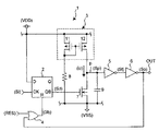
図3は、従来のパルス発生回路の回路例を示した図である(例えば、特許文献1参照。)。図3において、パルス発生回路100は、インバータ101、Dフリップフロップ102、電流出力コンパレータ103、コンパレータ104、ヒステリシス付きコンパレータ105及びコンデンサCを備えている。電流出力コンパレータ103には基準電圧V1が、コンパレータ104には基準電圧V4が、ヒステリシス付きコンパレータ105には基準電圧V2及びV3がそれぞれ供給されている。
FIG. 3 is a diagram illustrating a circuit example of a conventional pulse generation circuit (see, for example, Patent Document 1). In FIG. 3, the
図4は、図3のパルス発生回路100の動作例を示したタイミングチャートであり、図4を参照しながら図3のパルス発生回路100の動作例について説明する。インバータ101を介してパルス信号S1が入力されるDフリップフロップ102の出力信号S2は、電流出力コンパレータ103の非反転入力端に入力され、電流出力コンパレータ103の出力電流は、コンデンサCを充放電する。コンパレータ104の非反転入力端の電圧が基準電圧V4を超えると、コンパレータ104の出力信号の信号レベルが反転し、Dフリップフロップ102がリセットされる。
FIG. 4 is a timing chart showing an operation example of the
ここで、ヒステリシス付きコンパレータ105の出力信号が立ち上がるときの基準電圧V2及び立ち下がるときの基準電圧V3を、それぞれ基準電圧V4よりも小さい電圧にしておくと、ヒステリシス付きコンパレータ105の出力端からパルスを出力させることができる。このように、電流出力コンパレータ103からの定電流とコンパレータ104で、入力信号S1に対する出力信号S5の遅延時間が決定されており、カウンタ等を使用しなくても該遅延時間を精度よく設定することができる。
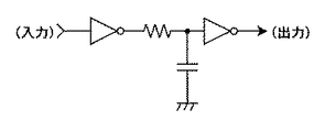
しかし、図3のような回路では、コンパレータが3つ必要であり、基準電圧V1〜V4を得るため精度の良い電圧源を必要とする。このため、回路規模が大きくなるという問題があった。回路規模を小さくするために図5のような回路も考えられるが、LSIにこのような回路を搭載した場合、電源電圧やプロセスパラメータの影響で遅延時間が大きく変化するという問題があった。 However, in the circuit as shown in FIG. 3, three comparators are required, and an accurate voltage source is required to obtain the reference voltages V1 to V4. Therefore, there is a problem that the circuit scale becomes large. In order to reduce the circuit scale, a circuit as shown in FIG. 5 is also conceivable. However, when such a circuit is mounted on an LSI, there is a problem that the delay time changes greatly due to the influence of the power supply voltage and process parameters.
本発明は、上記のような問題を解決するためになされたものであり、カレントミラー回路で設定した電流を用いて遅延時間を設定することにより、コンパレータや基準電圧生成回路を使用せずに回路規模を小さくすることができ、電源電圧の変動による遅延時間の変化を小さくすることができるパルス発生回路を得ることを目的とする。 The present invention has been made to solve the above-described problems, and by setting the delay time using the current set by the current mirror circuit, the circuit can be used without using a comparator or a reference voltage generation circuit. It is an object of the present invention to provide a pulse generation circuit that can be reduced in scale and that can reduce a change in delay time due to a change in power supply voltage.
この発明に係るパルス発生回路は、パルス信号からなる入力信号が入力されてから所定時間後にパルス信号を所定の出力端から出力するパルス発生回路において、
所定の定電流を生成して出力する定電流発生回路と、
該定電流発生回路からの定電流によって充電されるコンデンサと、
前記入力信号における信号レベルの所定の変化を検出するDフリップフロップ回路と、
該Dフリップフロップ回路の所定の出力端から出力される信号に応じて、前記コンデンサに充電又は放電を行わせる充放電切替回路と、
前記コンデンサに充電された電荷によって発生する電圧を2値の信号に変換して前記出力端に出力する変換回路と、
を備え、
前記変換回路の出力信号が、前記Dフリップフロップ回路のリセット信号入力端に入力され、変換回路の出力信号をDフリップフロップ回路のリセット信号入力端に帰還する帰還ループを形成するものである。
The pulse generation circuit according to the present invention is a pulse generation circuit that outputs a pulse signal from a predetermined output terminal after a predetermined time after an input signal consisting of a pulse signal is input,
A constant current generating circuit for generating and outputting a predetermined constant current;
A capacitor charged by a constant current from the constant current generating circuit;
A D flip-flop circuit for detecting a predetermined change in signal level in the input signal;
A charge / discharge switching circuit for charging or discharging the capacitor in accordance with a signal output from a predetermined output terminal of the D flip-flop circuit;
A conversion circuit that converts a voltage generated by the electric charge charged in the capacitor into a binary signal and outputs the signal to the output terminal;
With
The output signal of the conversion circuit is input to the reset signal input terminal of the D flip-flop circuit, and a feedback loop is formed that feeds back the output signal of the conversion circuit to the reset signal input terminal of the D flip-flop circuit.
具体的には、前記定電流発生回路は、入力端に定電流源が接続されたカレントミラー回路で構成されるようにした。 Specifically, the constant current generating circuit is constituted by a current mirror circuit having a constant current source connected to the input end.
また、前記充放電切替回路は、Dフリップフロップ回路の所定の出力端から出力された信号に応じて前記コンデンサの放電を行うトランジスタからなるようにした。 In addition, the charge / discharge switching circuit includes a transistor that discharges the capacitor in accordance with a signal output from a predetermined output terminal of the D flip-flop circuit.
また、前記Dフリップフロップ回路は、外部からのリセット信号又は前記変換回路の出力信号に応じて所定のリセット動作を行うようにしてもよい。 Further, the D flip-flop circuit may perform a predetermined reset operation in accordance with an external reset signal or an output signal of the conversion circuit.
本発明のパルス発生回路によれば、カレントミラー回路からなる定電流発生回路で設定した電流を用いて遅延時間を設定することができ、コンパレータや基準電圧生成回路を使用せずに回路規模を小さくすることができると共に電源電圧の変動による遅延時間の変化を小さくすることができる。 According to the pulse generation circuit of the present invention, the delay time can be set using the current set by the constant current generation circuit composed of a current mirror circuit, and the circuit scale can be reduced without using a comparator or a reference voltage generation circuit. In addition, the change in the delay time due to the fluctuation of the power supply voltage can be reduced.
次に、図面に示す実施の形態に基づいて、本発明を詳細に説明する。
第1の実施の形態.
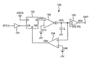
図1は、本発明の第1の実施の形態におけるパルス発生回路の回路例を示した図である。
図1において、パルス発生回路1は、Dフリップフロップ2、カレントミラー回路3、OR回路4、インバータ5,6、NMOSトランジスタ7、抵抗8及びコンデンサ9を備えている。更に、カレントミラー回路3は、PMOSトランジスタ11及び12で形成されている。なお、Dフリップフロップ2はDフリップフロップ回路を、カレントミラー回路3及び抵抗8は定電流発生回路を、インバータ5,6は変換回路を、NMOSトランジスタ7は充放電切替回路を、抵抗8は定電流源をそれぞれなす。
Next, the present invention will be described in detail based on the embodiments shown in the drawings.
First embodiment.
FIG. 1 is a diagram showing a circuit example of a pulse generation circuit according to the first embodiment of the present invention.
In FIG. 1, the
正側電源電圧VDDと負側電源電圧VSSとの間に、PMOSトランジスタ11と抵抗8が直列に接続される共にPMOSトランジスタ12とNMOSトランジスタ7が直列に接続されている。PMOSトランジスタ11及び12の各ゲートは接続され、該接続部がPMOSトランジスタ11のドレインに接続されている。NMOSトランジスタ7のゲートは、Dフリップフロップ2の反転出力端QBに接続され、NMOSトランジスタ7に並列にコンデンサ9が接続されている。
Between the positive power supply voltage VDD and the negative power supply voltage VSS, the PMOS transistor 11 and the resistor 8 are connected in series, and the
一方、PMOSトランジスタ12とNMOSトランジスタ7との接続部と出力端OUTとの間にはインバータ5及び6が直列に接続されている。更に、インバータ6の出力端は、OR回路4の一方の入力端に接続され、OR回路4の他方の入力端には外部からのリセット信号RESが入力されている。OR回路4の出力端は、Dフリップフロップ2のリセット信号入力端Rに接続され、Dフリップフロップ2の入力端Dには正側電源電圧VDDが入力され、Dフリップフロップ2のクロック信号入力端CKには外部からの入力信号Siが入力されている。
On the other hand,
このような構成において、OR回路4の出力信号をSbに、Dフリップフロップ2の出力端QBからの出力信号をSdにそれぞれすると共に、NMOSトランジスタ7、PMOSトランジスタ12、コンデンサ9及びインバータ5の入力端の接続部を接続部pとする。更に、インバータ5の出力信号をSfとすると共に、インバータ6の出力信号をSoとする。
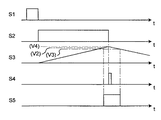
図2は、図1のパルス発生回路1の動作例を示したタイミングチャートであり、図2を参照しながら図1のパルス発生回路1の動作について説明する。なお、図2において、斜線で示した部分は、Dフリップフロップ2にリセットがかかる前の不定状態であることを示している。
In such a configuration, the output signal of the
FIG. 2 is a timing chart showing an operation example of the
リセット信号RESがハイ(High)レベルになると、Dフリップフロップ2にリセットがかかり、出力端Qはロー(Low)レベルに、反転出力端QBはハイレベルになる。このとき、NMOSトランジスタ7は、オンしてコンデンサ9の電荷を放電し、接続部pの電圧、すなわちインバータ5の入力端に入力される信号Spの電圧Vpを負側電源電圧VSSにする。このことから、インバータ5の出力信号Sfはハイレベルになると共にインバータ6の出力信号Soはローレベルになり、リセット信号RESがハイレベルからローレベルに戻ると、Dフリップフロップ2のリセット状態が解除され、この状態は入力信号Siの立ち上がりまで保たれる。
When the reset signal RES becomes high level, the D flip-
入力信号Siがローレベルからハイレベルに変わると、Dフリップフロップ2において、出力端Qはハイレベルに、反転出力端QBはローレベルにそれぞれ変化する。NMOSトランジスタ7はオフ状態になり、カレントミラー回路3の出力電流ipによってコンデンサ9が充電される。該出力電流ipは、PMOSトランジスタ11及び12のゲート幅W及びゲート長Lがそれぞれ同じで、β=μ0×Cox×W/L(ただし、μ0:移動度、Cox:単位面積当たりのゲート酸化膜容量とする)とした場合、下記(1)式で示すことができる。
ip=(β/2)×[[β×Vtp−1/R1+{(β×Vtp−1/R1)2−β×(β×Vtp2−2×VDD/R1)}1/2]/β−Vtp]2………………(1)
なお、VtpはPMOSトランジスタのしきい値(絶対値)を、R1は抵抗8の抵抗値をそれぞれ示している。
When the input signal Si changes from low level to high level, in the D flip-
ip = (β / 2) × [[β × Vtp-1 / R1 + {(β × Vtp-1 / R1) 2 -β × (β × Vtp 2 -2 × VDD / R1)} 1/2] / β -Vtp] 2 ……………… (1)
Vtp represents the threshold value (absolute value) of the PMOS transistor, and R1 represents the resistance value of the resistor 8.
前記電流ipでコンデンサ9を充電したときの接続部pの電圧Vpは、入力信号Siの信号レベルがローレベルからハイレベルになった時間、すなわちNMOSトランジスタ7がオフ状態になった時間を基準として、下記(2)式のように示すことができる。
Vp=(ip/C1)×t………………(2)
なお、tは時間を、C1はコンデンサ9の容量をそれぞれ示している。
The voltage Vp of the connection portion p when the
Vp = (ip / C1) × t (2)
Here, t represents time, and C1 represents the capacity of the
インバータ5のしきい値VthがVDD/2であるとすると、インバータ5の出力信号Sfがハイレベルからローレベルに反転する時間は、下記(3)式のように示すことができる。
t=(C1×VDD)/(2×ip)………………(3)
Assuming that the threshold value Vth of the
t = (C1 × VDD) / (2 × ip) (3)
インバータ5の出力信号Sfの信号レベルが反転してハイレベルからローレベルになると、インバータ6の出力信号Soはローレベルからハイレベルに信号レベルが反転する。出力信号Soが帰還され、OR回路4を介してDフリップフロップ2にリセットがかかると、再びDフリップフロップ2の出力端QBがハイレベルになる。このことにより、出力端OUTはローレベルになり、該状態は入力信号Siがハイレベルになるまで保たれる。
なお、電源電圧VDDが変化したとき、前記(3)式における分子(C1×VDD)が変化するが、前記(3)式の分母における電流ipは、前記(1)式のように分子の変化分とほぼ同じ割合で電源電圧VDDによって変化するため、結果として、電源電圧VDDによる遅延時間の変動の小さいパルス発生回路を実現することができる。
When the signal level of the output signal Sf of the
When the power supply voltage VDD changes, the numerator (C1 × VDD) in the equation (3) changes, but the current ip in the denominator of the equation (3) changes in the numerator as in the equation (1). As a result, it is possible to realize a pulse generation circuit with a small variation in delay time due to the power supply voltage VDD.
このように、本第1の実施の形態におけるパルス発生回路は、入力信号Siの変化を検出するDフリップフロップ2の反転出力信号Sdが入力されるNMOSトランジスタ7の動作によって、コンデンサ9に対してカレントミラー回路3からの電流ipによる充電又は放電が行われ、コンデンサ9に充電された電荷により発生する電圧Vpが入力されるインバータ5の出力信号Sfをインバータ6を介してDフリップフロップ2のリセット端子RESに帰還する帰還ループを形成するようにした。このことから、カレントミラー回路で設定した電流を用いて遅延時間を設定することができ、コンパレータや基準電圧生成回路を使用せずに回路規模を小さくすることができると共に電源電圧の変動による遅延時間の変化を小さくすることができる。
As described above, the pulse generation circuit according to the first embodiment is applied to the
1 パルス発生回路
2 Dフリップフロップ
3 カレントミラー回路
4 OR回路
5,6 インバータ
7 NMOSトランジスタ
8 抵抗
9 コンデンサ
11,12 PMOSトランジスタ
DESCRIPTION OF
Claims (4)
所定の定電流を生成して出力する定電流発生回路と、
該定電流発生回路からの定電流によって充電されるコンデンサと、
前記入力信号における信号レベルの所定の変化を検出するDフリップフロップ回路と、
該Dフリップフロップ回路の所定の出力端から出力される信号に応じて、前記コンデンサに充電又は放電を行わせる充放電切替回路と、
前記コンデンサに充電された電荷によって発生する電圧を2値の信号に変換して前記出力端に出力する変換回路と、
を備え、
前記変換回路の出力信号が、前記Dフリップフロップ回路のリセット信号入力端に入力され、変換回路の出力信号をDフリップフロップ回路のリセット信号入力端に帰還する帰還ループを形成することを特徴とするパルス発生回路。 In a pulse generation circuit that outputs a pulse signal from a predetermined output terminal after a predetermined time after an input signal consisting of a pulse signal is input,
A constant current generating circuit for generating and outputting a predetermined constant current;
A capacitor charged by a constant current from the constant current generating circuit;
A D flip-flop circuit for detecting a predetermined change in signal level in the input signal;
A charge / discharge switching circuit for charging or discharging the capacitor in accordance with a signal output from a predetermined output terminal of the D flip-flop circuit;
A conversion circuit that converts a voltage generated by the electric charge charged in the capacitor into a binary signal and outputs the signal to the output terminal;
With
The output signal of the conversion circuit is input to a reset signal input terminal of the D flip-flop circuit, and a feedback loop is formed that feeds back the output signal of the conversion circuit to the reset signal input terminal of the D flip-flop circuit. Pulse generation circuit.
4. The pulse generation circuit according to claim 1, wherein the D flip-flop circuit performs a predetermined reset operation in accordance with an external reset signal or an output signal of the conversion circuit.
Priority Applications (1)
| Application Number | Priority Date | Filing Date | Title |
|---|---|---|---|
| JP2003340939A JP2005109902A (en) | 2003-09-30 | 2003-09-30 | Pulse generation circuit |
Applications Claiming Priority (1)
| Application Number | Priority Date | Filing Date | Title |
|---|---|---|---|
| JP2003340939A JP2005109902A (en) | 2003-09-30 | 2003-09-30 | Pulse generation circuit |
Publications (1)
| Publication Number | Publication Date |
|---|---|
| JP2005109902A true JP2005109902A (en) | 2005-04-21 |
Family
ID=34535689
Family Applications (1)
| Application Number | Title | Priority Date | Filing Date |
|---|---|---|---|
| JP2003340939A Pending JP2005109902A (en) | 2003-09-30 | 2003-09-30 | Pulse generation circuit |
Country Status (1)
| Country | Link |
|---|---|
| JP (1) | JP2005109902A (en) |
Cited By (3)
| Publication number | Priority date | Publication date | Assignee | Title |
|---|---|---|---|---|
| US7804346B2 (en) | 2007-05-25 | 2010-09-28 | Samsung Electronics Co., Ltd. | Level converting flip-flop and method of operating the same |
| CN108649930A (en) * | 2018-04-24 | 2018-10-12 | 虹光精密工业股份有限公司 | short pulse generating circuit |
| CN114499181A (en) * | 2022-04-08 | 2022-05-13 | 惠科股份有限公司 | Drive circuit, light emitting circuit and display device |
-
2003
- 2003-09-30 JP JP2003340939A patent/JP2005109902A/en active Pending
Cited By (5)
| Publication number | Priority date | Publication date | Assignee | Title |
|---|---|---|---|---|
| US7804346B2 (en) | 2007-05-25 | 2010-09-28 | Samsung Electronics Co., Ltd. | Level converting flip-flop and method of operating the same |
| CN108649930A (en) * | 2018-04-24 | 2018-10-12 | 虹光精密工业股份有限公司 | short pulse generating circuit |
| CN108649930B (en) * | 2018-04-24 | 2022-05-03 | 虹光精密工业股份有限公司 | Short pulse generating circuit |
| CN114499181A (en) * | 2022-04-08 | 2022-05-13 | 惠科股份有限公司 | Drive circuit, light emitting circuit and display device |
| CN114499181B (en) * | 2022-04-08 | 2022-07-22 | 惠科股份有限公司 | Drive circuit, light emitting circuit and display device |
Similar Documents
| Publication | Publication Date | Title |
|---|---|---|
| JP2010166108A (en) | Delay circuit | |
| US20070182499A1 (en) | Oscillation circuit | |
| JP2007033180A (en) | Average current detection circuit | |
| JP4938439B2 (en) | Switching control circuit | |
| US8692623B2 (en) | Relaxation oscillator circuit including two clock generator subcircuits having same configuration operating alternately | |
| JP2010206650A (en) | Automatic adjustment oscillator | |
| JP2004128950A (en) | Power on reset circuit | |
| JP2006166305A5 (en) | ||
| US7280000B2 (en) | Apparatus and method for reducing power consumption within an oscillator | |
| JP2007312017A (en) | Oscillator circuit and semiconductor memory | |
| JP2007311969A (en) | Oscillation circuit | |
| US7545128B2 (en) | Regulator circuit | |
| JPH05111241A (en) | Dc/dc converter | |
| US7126434B2 (en) | Oscillator circuit for semiconductor device | |
| JP2005109902A (en) | Pulse generation circuit | |
| TWI285029B (en) | Delay stage insensitive to operating voltage and delay circuit including the same | |
| JP2007311968A (en) | Oscillation circuit | |
| JP3810316B2 (en) | Frequency multiplier circuit | |
| CN110943497B (en) | Charging and discharging circuit and oscillator | |
| CN110943496B (en) | Charging and discharging circuit and oscillator | |
| JP4829724B2 (en) | Oscillator circuit | |
| US5886550A (en) | Integrated circuit built-in type supply power delay circuit | |
| JP2005221256A (en) | Current detection circuit | |
| JP3129767B2 (en) | Oscillation stop detection circuit | |
| JP4353791B2 (en) | Pulse generator |