JP2005050349A - Method and device for optical input guidance - Google Patents
Method and device for optical input guidance Download PDFInfo
- Publication number
- JP2005050349A JP2005050349A JP2004223866A JP2004223866A JP2005050349A JP 2005050349 A JP2005050349 A JP 2005050349A JP 2004223866 A JP2004223866 A JP 2004223866A JP 2004223866 A JP2004223866 A JP 2004223866A JP 2005050349 A JP2005050349 A JP 2005050349A
- Authority
- JP
- Japan
- Prior art keywords
- detector
- light beam
- input guidance
- coherent
- image
- Prior art date
- Legal status (The legal status is an assumption and is not a legal conclusion. Google has not performed a legal analysis and makes no representation as to the accuracy of the status listed.)
- Pending
Links
Images


Classifications
-
- G—PHYSICS
- G06—COMPUTING; CALCULATING OR COUNTING
- G06F—ELECTRIC DIGITAL DATA PROCESSING
- G06F3/00—Input arrangements for transferring data to be processed into a form capable of being handled by the computer; Output arrangements for transferring data from processing unit to output unit, e.g. interface arrangements
- G06F3/01—Input arrangements or combined input and output arrangements for interaction between user and computer
- G06F3/03—Arrangements for converting the position or the displacement of a member into a coded form
- G06F3/0304—Detection arrangements using opto-electronic means
- G06F3/0317—Detection arrangements using opto-electronic means in co-operation with a patterned surface, e.g. absolute position or relative movement detection for an optical mouse or pen positioned with respect to a coded surface
Abstract
Description
本出願は動き検出装置に関し、さらに詳しくは、相対的な動きを判定する正反射像を用いる装置及びシステムならびに方法に関する。 The present application relates to motion detection devices, and more particularly to devices and systems and methods that use specular images to determine relative motion.
光学式相対的運動検出装置は、一般に、入力誘導装置(navigation device)が面上を通過する際或いは面が入力誘導装置を通過する際に面像を捕捉することで入力誘導装置と面の間の相対運動を割り出す像相関技法を用いる。面に対する入力誘導装置の相対運動の変位と方向は、一つの像を後続する像と比較することで割り出される。一般には面上に投影された陰に起因する強度変動を検出するが、この技法の感度と適用範囲は捕捉像の強度コントラストに依存する。相対運動入力誘導装置は、例えばコンピュータ画面ポインタ(例えば、マウス)制御に用いられる。 An optical relative motion detection device generally captures a surface image when an input navigation device passes over a surface or when a surface passes through the input guidance device, so that the space between the input guidance device and the surface is detected. An image correlation technique is used to determine the relative motion of. The displacement and direction of the relative motion of the input guidance device relative to the surface is determined by comparing one image with the following image. In general, intensity variations due to shadows projected onto a surface are detected, but the sensitivity and coverage of this technique depends on the intensity contrast of the captured image. The relative motion input guidance device is used, for example, for computer screen pointer (for example, mouse) control.
特許文献1、特許文献2、特許文献3、特許文献4、特許文献5、特許文献6には、光学式マウスや他のハンドヘルド入力誘導装置やハンドヘルドスキャナの実例が開示されている。これらの特許文献の開示内容の全ては、引用することにより、本明細書の一部をなすものとする。
一般の既存の光学式入力誘導装置には、入力誘導対象面を斜め方向から照明する発光ダイオード(LED)が用いられる。ほぼ5〜500μmの面上の高さ変動は、幾何的な光線光学系により描かれる陰を投影する。シャドーバターン像の大きさとコントラストは、高さ変動の大きさを通じて面の種別に一部依存する。一般に、検出器は面に垂直な方向の反射を受光するよう位置決めしてあり、面と入射光の間の角度は通常は暗視野像処理に似たシャドーバターン像のコントラストを最適化するよう選択される。入射角の一般的な値は、約5度〜約20度の範囲にある。 A general existing optical input guidance device uses a light emitting diode (LED) that illuminates an input guidance target surface from an oblique direction. A height variation on the surface of approximately 5 to 500 μm projects shadows drawn by the geometric ray optics. The size and contrast of the shadow pattern image depend in part on the type of surface through the height variation. In general, the detector is positioned to receive reflections in a direction perpendicular to the surface, and the angle between the surface and the incident light is usually chosen to optimize shadow pattern contrast similar to dark field image processing Is done. Typical values for the angle of incidence are in the range of about 5 degrees to about 20 degrees.
白板等の平滑面や高光沢紙やプラスチックや塗装金属は、一般の現行の光学式入力誘導装置に対し機能的な難題を提起する。一般に、平滑面には中間空間周波数の構造が殆ど含まれず、高い空間周波数の構造が多く含まれる。信号レベルを増やすにはLED照明には大電力が必要であり、30mAを超える電流消費を招く。 Smooth surfaces such as white boards, high gloss paper, plastics and painted metals pose functional challenges for common current optical input guidance devices. In general, the smooth surface contains almost no intermediate spatial frequency structure and many high spatial frequency structures. In order to increase the signal level, the LED illumination requires a large amount of power, which causes a current consumption exceeding 30 mA.
本発明によれば、予め選択した角度範囲の反射光を光学式入力誘導装置の検出器により捕捉する。典型的には、光学式入力誘導装置の検出器は面からの鏡面反射を捕捉するよう位置決めされる。鏡面反射は、シャドーバターン像とスペックルパターンのいずれとも異なる像を生成する。鏡面反射は一般に、シャドーバターン像手法に比べより良好な信号をもたらす。これにより、非常に平滑な面においてさえも高コントラストの像が得られるようになる。その上、ランバート面(均等拡散面)と比べて画質が保存される。何故なら光は依然として鏡面反射方向に散乱するからである。正反射像は、照明源の波長に依存する。すなわち、一般に照明源の帯域が低下するにつれ正反射像のコントラストは高まり、それ故にレーザーに基づく照明が最高のコントラストをもたらす。 According to the present invention, the reflected light in the preselected angle range is captured by the detector of the optical input guidance device. Typically, the detector of the optical input guidance device is positioned to capture specular reflections from the surface. The specular reflection generates an image different from both the shadow pattern image and the speckle pattern. Specular reflection generally yields a better signal than the shadow pattern image technique. As a result, a high-contrast image can be obtained even on a very smooth surface. In addition, the image quality is preserved compared to the Lambertian surface (uniform diffusion surface). This is because light is still scattered in the specular direction. The specular image depends on the wavelength of the illumination source. That is, the contrast of the specular image generally increases as the bandwidth of the illumination source decreases, and therefore laser-based illumination provides the highest contrast.
本発明によれば、検出器が入力誘導対象面の上方或いは下方に横たわる空間内の結像面にある非合焦光学構造の用途が開示される。垂直キャビティ面発光レーザー(VCSEL)から得られるコヒーレント照明を用い、面入力誘導用に高コントラスト正反射像を生成する。 According to the present invention, the use of a non-focusing optical structure in which the detector is on the imaging plane in the space lying above or below the input guidance target surface is disclosed. A high-contrast specular image is generated for surface input guidance using coherent illumination obtained from a vertical cavity surface emitting laser (VCSEL).
平滑面上に光束を入射させた場合、入射束の光線は反射され、平滑面を離れる際は束に集められたままである。しかしながら、面が微視的に粗い場合、そのときは光線は多くの異なる方向へ反射され散乱される。面の粗さに対応する空間周波数は、照明波長のオーダーとなることもある。各個別光線は、反射の法則に従う。しかしながら、粗面の場合には各個別光線は異なる向きを有する面の一部と出会う。それ故、異なる入射光線ごとに面法線は異なる。このため、個々の光線が反射の法則に従って反射すると、個々の光線は異なる方向へ散乱する。さらに、コヒーレント照明或いは準コヒーレント照明を適用したときに、被反射光および散乱光の中で干渉により生成される高コントラスト強度パターンを正反射像内で観察することができる。干渉効果は、像に対し入力誘導に向けた改善されたコントラストをもたらす。 When a light beam is incident on a smooth surface, the light rays of the incident bundle are reflected and remain collected in the bundle when leaving the smooth surface. However, if the surface is microscopically rough, then the rays are reflected and scattered in many different directions. The spatial frequency corresponding to the surface roughness may be on the order of the illumination wavelength. Each individual ray follows the law of reflection. However, in the case of a rough surface, each individual ray meets a part of the surface having a different orientation. Therefore, the surface normal is different for different incident rays. For this reason, when individual rays are reflected according to the law of reflection, the individual rays are scattered in different directions. Further, when coherent illumination or quasi-coherent illumination is applied, a high contrast intensity pattern generated by interference among reflected light and scattered light can be observed in a regular reflection image. The interference effect results in improved contrast towards input guidance for the image.
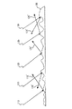
図1a〜図1cは、異なる種の面からの光の反射を例示するものである。図1aは、ランバート面140からビームパターン136への光ビーム135の反射を示す。ランバート面は完全散乱面であり、どんな小さな面要素からの所与の方向へ発する光の強度も面140に対する法線199の角度の余弦に比例する。図1bは、鏡面反射面150から角度θr=θiのビーム146への光ビーム145の反射を示すものであり、ただしこの角度は面法線199に対して規定してある。図1cは、面160からビーム156へ反射する光ビーム155を示す。面160は面140と面150の間の面特徴内に介在しており、ビームパターン156に対する均等拡散要素だけでなく鏡面反射成分も存在する。
1a-1c illustrate the reflection of light from different types of surfaces. FIG. 1 a shows the reflection of the
鏡面反射が光学的スペックルに関係しないことに留意することは、重要である。入力誘導対象面から反射した鏡面反射パターンの強度は、コヒーレント光或いは準コヒーレント光から生ずる。本発明により得られる、特徴が多く含まれる強度パターンは異種の面ごとに著しく変化し、特定の面に対しほぼ1対1の相関を有する。対照的に、スペックル像は本来が非常に統計的なものであり、第1近似では異なる面ごとに変動することはない。スペックル像は、面の可視の特徴との1対1の対応が限られたものである像パターンを呈する。コヒーレント光を被写体に照射するときはいつでもスペックルは存在するが、光学的スペックルの平均的な寸法は一般の光学式入力誘導用途向けの撮像配列の画素寸法よりも通常小さい。画素寸法が平均的なスペックル寸法よりも相当に大きいと、スペックルを光学式入力誘導のための信頼に足るパターンとして用いることができない。何故なら検出器配列の画素に複数の明暗のスペックルの特徴が入射し、画素領域全体に平均化されてしまうからである。例えば、f値10の結像システム及び850nmで作動するレーザー光源を採用するなら、以下の式を用いて平均スペックル寸法=8.5μmが得られる。すなわち、平均スペックル寸法=f×λ、ただしfはf値で、λは波長である。ここでは、60μmの画素寸法をもった一般的な検出器配列を採用すると、検出器配列の各画素は49個を超えるスペックルを撮像することとなる。結果として平均化されることにより、スペックル分布から潜在的に入力誘導可能な特徴が取り除かれる。 It is important to note that specular reflection is not related to optical speckle. The intensity of the specular reflection pattern reflected from the input guidance target surface is generated from coherent light or quasi-coherent light. The intensity pattern including many features obtained by the present invention changes significantly for different surfaces, and has a substantially one-to-one correlation with a specific surface. In contrast, speckle images are inherently very statistical and do not vary from one surface to another in the first approximation. The speckle image presents an image pattern that has a limited one-to-one correspondence with the visible features of the surface. Speckle is present whenever a subject is irradiated with coherent light, but the average size of the optical speckle is usually smaller than the pixel size of an imaging array for general optical input guidance applications. If the pixel size is much larger than the average speckle size, the speckle cannot be used as a reliable pattern for optical input guidance. This is because a plurality of bright and dark speckle features are incident on the pixels of the detector array and averaged over the entire pixel area. For example, if an imaging system with an f-value of 10 and a laser light source operating at 850 nm are employed, an average speckle dimension = 8.5 μm is obtained using the following equation: That is, the average speckle dimension = f × λ, where f is the f value and λ is the wavelength. Here, when a general detector array having a pixel size of 60 μm is employed, each pixel in the detector array captures more than 49 speckles. The resulting averaging removes potentially input-inducible features from the speckle distribution.
図1dは、本発明による粗面105からの散乱を示す簡単な図である。入射光ビームの入射光線110,115,120,125,130はそれぞれ反射の法則に従い、粗面105からの反射光線110’,115’,120’,125’,130’となり、反射時に散乱させられる。本願明細で述べる光とは、約1ナノメータ(nm)から約1ミリメータ(mm)へ広がる波長範囲に亙る電磁放射を含むことを意図するものである。
FIG. 1d is a simple diagram illustrating scattering from a
図2は、本発明による面からの鏡面反射のより詳細な図を示す。入射光線205は、面220による反射前は角度座標φi,θiを有する。一般に、面220は微視的な粗さすなわち被反射光の反射角に影響を及ぼす光学的な不規則性を有するものである。被反射光線210がφro±δφr,θro±δθrにより規定される円錐角内に在る場合、光線205に対応する面要素が検出器により捕捉されることになる。
FIG. 2 shows a more detailed view of specular reflection from a surface according to the present invention. The
図3aは、入力誘導向け鏡面反射の使用に基づく光学式入力誘導システム300用の本発明による高水準ブロック線図である。面330は、光源装置304からの光ビーム398により照明する。鏡面反射光のビーム399は面330で反射され、プロセッサ320へ行く信号370を生成する検出器配列装置311により検出される。プロセッサ320は、信号370に応答して出力信号375を出力する。出力信号は、例えばコンピュータ画面上でのポインタの位置駆動に用いることができる。プロセッサ320は、光学式入力誘導装置303の一部とするか、或いは光学式入力誘導システム300内の何処かに配置することができる。本発明によれば、光学式入力誘導装置303の一部実施形態は手で動かすことのできるコンピュータシステム内の光学式マウスとすることができる。
FIG. 3a is a high level block diagram according to the present invention for an optical
図3bは、本発明の一実施形態による光学式入力誘導装置303用の構成要素の略図を示す。光源305、すなわち光源装置304(図3a参照)の一部は面法線350に対し入射角θiで位置決めされており、レンズ301に入射する光ビーム315を供給してビーム315’を生成する。レンズ301は主にビーム315用の集光効率を改善する働きをし、レンズ301は任意選択的である。レンズ301は、例えばコリメーションレンズとすることができる。しかしながら、例えば光源305がVCSEL或いはエッジ発光レーザー等のコヒーレント光源である場合、ビーム315を平行光束化する必要はない。コヒーレント光源の使用により、反射光線365間のコヒーレント干渉が故の改善された像コントラストがもたらされる。
FIG. 3b shows a schematic diagram of the components for the optical
光源305が狭帯域発光LED(発光ダイオード)や狭帯域フィルタ付きLED等の準コヒーレント光源である場合、そのときは平滑面上の入力誘導用にレンズ301或いは制限アパチャが必要となろう。制限アパチャの使用は面330への入射パワーを低減するが、空間的コヒーレンスを改善する。レンズ301を用いた場合、レンズ301は回折レンズ或いは屈折レンズ又は他の適当な光学素子とすることができ、性能を改善すべく光学的コーティングを施すことができる。従来の狭帯域発光LEDと併せた狭アパチャの使用に代え、光源として狭帯域エッジ発光LEDを用いることもできる。
If the
本明細書の記載では、検出器は光子を電気信号へ変換する装置となるよう規定してある。検出器配列310、すなわち検出器配列装置311の一部(図3a参照)はθr≒θiとなるよう選択された反射角θrに位置決めしてある。θr≒θiを有する面330からの被反射光線365だけがビーム317を作り上げ、検出器配列310によって受光される。本発明の一実施形態によれば、面330の被照明部分がレンズ307により結像される。面330上の点316は、レンズ307により検出器配列310上の点316’に結像される。これ故、結像光学系により310による像の捕捉が可能となる。コヒーレント光源により生成された像には、一般に面による特徴と干渉による特徴が含まれる。像内のスペックルの存在は、本発明による入力誘導用には用いない。干渉による特徴は、鏡面反射場の個々の光線をコヒーレントに加算することにより生ずる。結像レンズ307は、回折レンズ或いは屈折レンズ又は面330の一部を結像させる他の適当な光学素子とすることができ、性能を改善すべく誘電体薄膜によって光学的コーティングを行なうことができる。光源305は一般的にはVCSEL(垂直キャビティ面発光レーザー)やエッジ発光レーザー等の狭帯域レーザー光源であるが、狭帯域LEDとすることもでき、その一方で検出器配列310は一般的にCCDやCMOSやGaAsや非晶質シリコンや他の適当な検出器配列とすることができる。検出器配列310の性能は、検出器配列310に対し反射防止誘電体コーティングを施すことで改善することができる。
In the description herein, the detector is defined to be a device that converts photons into electrical signals. The
より高い面コントラスト及び解像度を有することで、光学式入力誘導装置303はより平滑な面上で入力誘導できるようになる。有効解像度は、面330等の入力誘導面の最小の解像可能な特徴として規定される。有効解像度は、光学伝達関数と光学系倍率と検出器配列310等の検出器配列の有効画素寸法とに依存する。倍率を固定した場合、より高い面解像度には例えば検出器配列310がより小さな画素を有することが必要とされる。光学式入力誘導装置303に関する面330上の最大の入力誘導速度は、相互相関計算のための処理時間だけでなく検出器配列310のフ最大フレームレートによっても制限される。面330に対する光学式入力誘導装置303の物理的変位は、有効画素寸法を単位として計測される。このことは、光学式入力誘導装置303の検出器列310の画素寸法を減少させた場合に、光学式入力誘導装置303の応答性或いは最大入力誘導速度が減少することを意味する。一般に、検出器配列310とプロセッサ320と全体の電力消費のコストと所望の応答性との間の兼ね合いを考慮し、本発明による実施形態ごとに面解像度及び光学倍率に達するよう釣り合いを取る。
By having higher surface contrast and resolution, the optical
本発明の一実施形態によれば、光学式入力誘導装置303が面330に対し移動する際に、光学式入力誘導装置303と面330の間の異なる相対位置にて散乱パターンが生成される。検出器配列310の視野内にある面330からの鏡面反射により、各散乱パターンが生成される。散乱パターン像は、光源305の波長に強く依存する。一般に、光源305の波長は検出器配列310のピークに合わせて選択される。像コントラスト及び信号は一般に従来技術のシャドーバターン光学式入力誘導システムを上回るように改善されるため、より短い像蓄積時間が必要になり、より高いフレームレートでの獲得を可能になり、より高速での入力誘導が可能になる。
According to one embodiment of the present invention, as the optical
連続的に保存した正反射像をプロセッサ320内で比較することで、面330に対する光学式入力誘導装置300の相対的な動きを割り出すことができる。連続する散乱パターン像の相関は通常、相対的な動きの変位を割り出すのに用いられる。連続的に捕捉された散乱パターン像は、一部が互いに重複している。これ故に、プロセッサ320は各散乱パターン像の特徴を識別し、相対的な動きの変位と方向を算出する。連続的な散乱パターン像を保存することで、標準的な像相関アルゴリズムを用いてプロセッサ320により重複特徴を識別して方向と変位をもたらすことができる。さらなる詳細は、例えば、引用することにより本明細書の一部をなすものとした米国特許第5,786,804号に見出すことができる。本発明によれば、例えばガラス等の、非常に平滑ではあるが光学的に研磨されてはいない面の上でさえ相対的な動きを割り出すことができる。
By comparing the continuously stored specular images in the
コヒーレント光源を用いると、正反射像のコヒーレント干渉性が入力誘導用の高コントラスト強度パターンをもたらし、これにより検出器に対する面の結像は必要なくなる。図3cは、公称の像面335が面330に一致しない本発明による実施形態の略図を示す。公称の像面335が面330の上方にあるのと同様、レンズ306は公称の像面335が面330の下方にあるよう選択することもできる。面330上の面強度と高さ変動は、ビーム317の振幅及び位相変調を招く。被反射光線366間のコヒーレント干渉は、スカラー回折理論により記述することのできる強度パターンを生み出す。公称の像面335が面330に合致していない図3cに示す非合焦状態下にあっては、撮像器310が検出する強度パターンは鏡面反射コヒーレント光場の回折パターンであり、図3dを参照し、式(1)の公知のフレネル−キルヒホッフ(Fresnel−Kirchhoff)積分にて与えられる。

U(x’,y’,z1)は観察面392のスカラー場であり、U0は光源面390の場の振幅であり、Ωはアパチャ391の積分領域を表わす。強度Iは、I=|U|2によって与えられ、アパチャ391を通過する全ての光線396のコヒーレントな加算により割り出される。例えば、図3cに関しては、アパチャ391は面330の被照明部分に対応する。面330の被照明部分の回折像は式(1)により記述され、本発明の一実施形態における面330上での入力誘導に用いられる。
U (x ′, y ′, z 1 ) is a scalar field on the
面330上での入力誘導用に回折像を使用することにより、一般に準周期的面特徴により引き起こされるであろう問題を避けることができる。図4aは、木材粒子含有面440a,440bと文字含有面445a,445bとホログラフ的パターン含有面450a,450bの例示像を示す。図4aの面440a,445a,450aの像は合焦されたものであるのに対し、面440b,445b,450bの像は非合焦のものである。入力誘導装置303と面330の間の相対的な動きは、連続的に捕捉された像間の相互相関から割り出される。図4aに示したような周期的或いは単一方向のパターンは、一般に相互相関計算における複数ピークが原因で動き検出アルゴリズムに対し問題を生み出す。この種の問題の低減は一般に、相互相関の適用前に捕捉像に対する特別な像処理アルゴリズム及びフィルタの適用を必要とする。光学式入力誘導システム300を合焦させないことで、図4bの面440b,445b,450bの図に見られる如く強度パターンはぼやけてしまい、すなわち低域濾波される。しかしながら、像のコントラストは回折像のコヒーレント干渉特性のお陰で高いままである。このため、非合焦光学式入力誘導システム300により、入力誘導装置303は大規模な像処理の導入を必要とすることなく多種多様な面について良好に機能させることができる。
By using a diffractogram for input guidance on the
図4bは、光学式マウス425が固定面430上を動く本発明によるシステム400を表わす図である。光学式マウスは通常、図3aの検出器配列装置311等の検出器配列装置を含む。一連の正反射像は通常、プロセッサ320(図3参照)により光学式マウス425内の位置情報へ変換され、矢印等の位置ポインタとして映像画面470上の表示用に中央処理装置475へ無線或いは有線で送信される。あるいは、生のまたは中間のデータを検出器配列装置311(図3a参照)から中央処理装置475へ送信して処理することができる。無線接続は高周波或いは赤外線のいずれかであり、本発明による光学式マウス425の無線実施形態は、例えば再充電可能な電池や燃料電池や太陽電池により給電することができる。
FIG. 4 b is a diagram representing a
図5は、本発明による光学式入力誘導装置500の一実施形態を示す。パッケージ化したVCSELとセンサダイ510はディスクリートであり、成形プラスチック構造515に一体化形成したコリメーションレンズ520と結像レンズ525を備えた光源として機能する。センサダイ535には、前記の検出器配列310等の検出器配列が組み込んである。成形プラスチック構造へのコリメーションレンズ520とレンズ525の一体化は、製造を簡単化しコストを低減する。センサダイ535内の検出器配列はビーム595の入射角θiに等しい反射角θrの光を受光するよう位置決めしてあり、それによって検出器配列からの生成信号が鏡面反射を表わすものとなる。センサダイ535は、ビーム595が検出器配列の面に垂直に入射するよう配向することができる。
FIG. 5 shows an embodiment of an optical
図6は、本発明による光学式入力誘導装置600の一実施形態を示す。一体型VCSEL610のダイは、成形プラスチック構造615に一体化形成したコリメーションレンズ620及びレンズ625を有する光源として機能する。センサダイ635には、前記の検出器配列310等の検出器配列が組み込んである。成形プラスチック構造へのコリメーションレンズ620及び結像レンズ625の一体化は、製造を簡単化し、コストを低減する。ビーム695はコリメーションレンズ620を垂直に通過し、全反射面675にて反射され、入射角θiで面650に入射する。センサダイ635の検出器配列はビーム695の入射角θiに等しい反射角θrの光を受光するよう位置決されており、それによって検出器配列からの生成信号が鏡面反射を表わすことを保証している。ビーム695が検出器配列の平面に垂直に入射するよう、センサダイ635を配向することができる。
FIG. 6 shows an embodiment of an optical
図7は、本発明による光学式入力誘導システム303の使用法に含まれるステップを示すフローチャートである。ステップ701において、面303は入射角角度θiの狭帯域光ビーム398により照らされる。ステップ702において、検出器配列311は入射角θiに等しいか又は近い反射角θrの被反射狭帯域光ビーム399を検出する。ステップ703において、狭帯域光ビーム399に応答して検出器配列311により像信号を生成する。ステップ704において、プロセッサ320により像信号を処理する。ステップ705において、像信号370に応答して出力信号375を出力し、例えば映像画面470上での位置ポインタの制御に用いることができる。
FIG. 7 is a flowchart illustrating the steps involved in using the optical
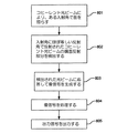
図8は、本発明による光学式入力誘導システム303の使用法に含まれるステップを示すフローチャートである。ステップ801において、面303は入射角θiのコヒーレント光ビーム398によリ照らされる。ステップ802において、検出器配列311が入射角θiに等しいか又は近い反射角θrの被反射光ビーム399を検出する。ステップ803において、光ビーム399に応答して検出器配列311により像信号を生成する。ステップ804において、プロセッサ320により像信号を処理する。ステップ805において、像信号370に応答して出力信号375を出力し、例えば映像画面470上の位置ポインタの制御に用いることができる。
FIG. 8 is a flowchart illustrating the steps involved in using the optical
本発明は特定の実施形態と併せ説明してきたが、前述の説明に照らし多くの代替例と改変例と変形例が明らかになろうことは当事者には明白である。従って、本発明は添付の特許請求の範囲の趣旨ならびに範囲に包含される代替例や改変例や変形例等の他の全てを含むことを意図するものである。 While the invention has been described in conjunction with specific embodiments, it will be apparent to those skilled in the art that many alternatives, modifications, and variations will become apparent in light of the foregoing description. Accordingly, the present invention is intended to embrace all other such alternatives, modifications and variations that fall within the spirit and scope of the appended claims.
300 光学式入力誘導システム
303 光学式入力誘導装置
304 光源装置
305 光源
306,307 レンズ
310 撮像器
DESCRIPTION OF
Claims (20)
前記面に対しある反射角に配置され、前記面からの前記光ビームの反射部分を受光するよう動作可能な検出器であって、前記反射角が前記照明角度にほぼ等しい前記検出器と
を備えてなる光学式入力誘導装置。 A coherent light source that illuminates the surface with a light beam at an illumination angle with respect to the surface;
A detector disposed at a reflection angle relative to the surface and operable to receive a reflected portion of the light beam from the surface, the detector having the reflection angle substantially equal to the illumination angle. An optical input guidance device.
コヒーレント鏡面反射干渉像を生成する手段であって、該干渉像のそれぞれは、前記マウスが移動する前記面の部分に特有のものである、前記手段と、
前記コヒーレント鏡面反射干渉像を、前記マウスと前記面との間の相対的な動きに対応する信号へと変換する手段と
を備えてなるシステム。 A system for controlling a position pointer on a video screen of a computer using a mouse that detects a relative movement with respect to a certain surface,
Means for generating a coherent specular reflection interference image, each of the interference images being specific to the portion of the surface on which the mouse moves;
Means for converting the coherent specular reflection interference image into a signal corresponding to a relative movement between the mouse and the surface.
前記面に対しある照明角度でコヒーレント光ビームを供給し、前記面を照らすステップと、
前記コヒーレント光ビームの鏡面反射部分を前記面に対するある反射角で受光し、前記反射角が前記照明角度にほぼ等しくなるようにするステップと
を含んでなる方法。 A method of determining relative movement between an optical input guidance device and a surface,
Providing a coherent light beam at an illumination angle relative to the surface to illuminate the surface;
Receiving a specular reflection portion of the coherent light beam at a reflection angle with respect to the surface, such that the reflection angle is substantially equal to the illumination angle.
Applications Claiming Priority (2)
| Application Number | Priority Date | Filing Date | Title |
|---|---|---|---|
| US10/630,169 US7321359B2 (en) | 2003-07-30 | 2003-07-30 | Method and device for optical navigation |
| US10/680,525 US7161682B2 (en) | 2003-07-30 | 2003-10-06 | Method and device for optical navigation |
Publications (2)
| Publication Number | Publication Date |
|---|---|
| JP2005050349A true JP2005050349A (en) | 2005-02-24 |
| JP2005050349A5 JP2005050349A5 (en) | 2007-07-26 |
Family
ID=33544785
Family Applications (1)
| Application Number | Title | Priority Date | Filing Date |
|---|---|---|---|
| JP2004223866A Pending JP2005050349A (en) | 2003-07-30 | 2004-07-30 | Method and device for optical input guidance |
Country Status (4)
| Country | Link |
|---|---|
| EP (1) | EP1503275A3 (en) |
| JP (1) | JP2005050349A (en) |
| CN (1) | CN1591468B (en) |
| TW (1) | TWI258706B (en) |
Cited By (7)
| Publication number | Priority date | Publication date | Assignee | Title |
|---|---|---|---|---|
| JP2007052025A (en) * | 2005-08-16 | 2007-03-01 | Avago Technologies Ecbu Ip (Singapore) Pte Ltd | System and method for optical navigation device having sliding function constituted so as to generate navigation information through optically transparent layer |
| JP2008003650A (en) * | 2006-06-20 | 2008-01-10 | Avago Technologies Ecbu Ip (Singapore) Pte Ltd | Pointing device |
| DE102008010945A1 (en) | 2007-02-26 | 2008-09-04 | Avago Technologies Ecbu Ip (Singapore) Pte. Ltd. | pointing device |
| JP2009140468A (en) * | 2007-07-27 | 2009-06-25 | Avago Technologies Ecbu Ip (Singapore) Pte Ltd | System and method for performing optical navigation on glass-like navigation surfaces |
| US7715016B2 (en) | 2005-12-15 | 2010-05-11 | Chung Shan Institute Of Science And Technology | Image invariant optical speckle capturing device and method |
| JP2011501318A (en) * | 2007-10-22 | 2011-01-06 | アバゴ・テクノロジーズ・ジェネラル・アイピー(シンガポール)プライベート・リミテッド | Optical mouse |
| KR101053369B1 (en) | 2010-05-11 | 2011-08-01 | 삼성전기주식회사 | Optical pointing module having lighting function and electronic device |
Families Citing this family (4)
| Publication number | Priority date | Publication date | Assignee | Title |
|---|---|---|---|---|
| US8847888B2 (en) | 2007-12-18 | 2014-09-30 | Microsoft Corporation | Optical mouse with limited wavelength optics |
| US20090160772A1 (en) * | 2007-12-20 | 2009-06-25 | Microsoft Corporation | Diffuse optics in an optical mouse |
| US20090160773A1 (en) * | 2007-12-20 | 2009-06-25 | Microsoft Corporation | Optical mouse |
| CN108828887B (en) * | 2018-06-05 | 2023-10-24 | 奥比中光科技集团股份有限公司 | Projector and depth camera |
Citations (5)
| Publication number | Priority date | Publication date | Assignee | Title |
|---|---|---|---|---|
| JPS63298428A (en) * | 1987-05-28 | 1988-12-06 | Nisshin Koki Kk | Optical mouse |
| JPH0313534U (en) * | 1989-06-23 | 1991-02-12 | ||
| JPH11345076A (en) * | 1998-04-30 | 1999-12-14 | Hewlett Packard Co <Hp> | Screen pointer position controller |
| JP2000020230A (en) * | 1998-07-02 | 2000-01-21 | Mitsubishi Electric Corp | Optical mouse scanner |
| JP2000508430A (en) * | 1998-03-09 | 2000-07-04 | オーティーエム テクノロジーズ リミテッド | Optical measurement of translation |
Family Cites Families (4)
| Publication number | Priority date | Publication date | Assignee | Title |
|---|---|---|---|---|
| US4794384A (en) * | 1984-09-27 | 1988-12-27 | Xerox Corporation | Optical translator device |
| US6424407B1 (en) * | 1998-03-09 | 2002-07-23 | Otm Technologies Ltd. | Optical translation measurement |
| KR20020050787A (en) * | 2000-12-21 | 2002-06-27 | 이형도 | Optical mouse |
| CN2560031Y (en) * | 2002-06-25 | 2003-07-09 | 陈淑芬 | Improved optical mouse |
-
2004
- 2004-04-26 EP EP04009854A patent/EP1503275A3/en not_active Withdrawn
- 2004-04-28 TW TW93111873A patent/TWI258706B/en active
- 2004-07-29 CN CN 200410070345 patent/CN1591468B/en active Active
- 2004-07-30 JP JP2004223866A patent/JP2005050349A/en active Pending
Patent Citations (5)
| Publication number | Priority date | Publication date | Assignee | Title |
|---|---|---|---|---|
| JPS63298428A (en) * | 1987-05-28 | 1988-12-06 | Nisshin Koki Kk | Optical mouse |
| JPH0313534U (en) * | 1989-06-23 | 1991-02-12 | ||
| JP2000508430A (en) * | 1998-03-09 | 2000-07-04 | オーティーエム テクノロジーズ リミテッド | Optical measurement of translation |
| JPH11345076A (en) * | 1998-04-30 | 1999-12-14 | Hewlett Packard Co <Hp> | Screen pointer position controller |
| JP2000020230A (en) * | 1998-07-02 | 2000-01-21 | Mitsubishi Electric Corp | Optical mouse scanner |
Cited By (11)
| Publication number | Priority date | Publication date | Assignee | Title |
|---|---|---|---|---|
| JP2007052025A (en) * | 2005-08-16 | 2007-03-01 | Avago Technologies Ecbu Ip (Singapore) Pte Ltd | System and method for optical navigation device having sliding function constituted so as to generate navigation information through optically transparent layer |
| US7715016B2 (en) | 2005-12-15 | 2010-05-11 | Chung Shan Institute Of Science And Technology | Image invariant optical speckle capturing device and method |
| JP2008003650A (en) * | 2006-06-20 | 2008-01-10 | Avago Technologies Ecbu Ip (Singapore) Pte Ltd | Pointing device |
| US7511825B2 (en) | 2006-06-20 | 2009-03-31 | Avago Technologies Ecbu Ip (Singapore) Pte. Ltd. | Pointing device |
| DE102008010945A1 (en) | 2007-02-26 | 2008-09-04 | Avago Technologies Ecbu Ip (Singapore) Pte. Ltd. | pointing device |
| DE102008010945A9 (en) | 2007-02-26 | 2009-02-19 | Avago Technologies Ecbu Ip (Singapore) Pte. Ltd. | pointing device |
| US7791735B2 (en) | 2007-02-26 | 2010-09-07 | Avago Technologies Ecbu Ip (Singapore) Pte. Ltd. | Pointing device |
| JP2009140468A (en) * | 2007-07-27 | 2009-06-25 | Avago Technologies Ecbu Ip (Singapore) Pte Ltd | System and method for performing optical navigation on glass-like navigation surfaces |
| JP4684320B2 (en) * | 2007-07-27 | 2011-05-18 | アバゴ・テクノロジーズ・イーシービーユー・アイピー(シンガポール)プライベート・リミテッド | System and method for performing optical navigation on a glassy navigation surface |
| JP2011501318A (en) * | 2007-10-22 | 2011-01-06 | アバゴ・テクノロジーズ・ジェネラル・アイピー(シンガポール)プライベート・リミテッド | Optical mouse |
| KR101053369B1 (en) | 2010-05-11 | 2011-08-01 | 삼성전기주식회사 | Optical pointing module having lighting function and electronic device |
Also Published As
| Publication number | Publication date |
|---|---|
| CN1591468A (en) | 2005-03-09 |
| CN1591468B (en) | 2010-05-26 |
| EP1503275A2 (en) | 2005-02-02 |
| TWI258706B (en) | 2006-07-21 |
| TW200504604A (en) | 2005-02-01 |
| EP1503275A3 (en) | 2006-08-09 |
Similar Documents
| Publication | Publication Date | Title |
|---|---|---|
| US7161682B2 (en) | Method and device for optical navigation | |
| US9826216B1 (en) | Systems and methods for compact space-time stereo three-dimensional depth sensing | |
| US7116427B2 (en) | Low power consumption, broad navigability optical mouse | |
| US7244925B2 (en) | Compact and low profile optical navigation device | |
| US7773070B2 (en) | Optical positioning device using telecentric imaging | |
| JPH1065882A (en) | Method for acquiring medium surface shape data | |
| JP2005302036A (en) | Optical device for measuring distance between device and surface | |
| JPH11118475A (en) | Control of robot grip and method and device for starting guide based on contrast | |
| JP4335218B2 (en) | Speckle capture device, optical mouse and speckle capture method | |
| JP2005050349A (en) | Method and device for optical input guidance | |
| US7440119B2 (en) | Three-dimensional shape detecting device, image capturing device, and three-dimensional shape detecting method | |
| EP2240761A2 (en) | Information processing apparatus and method | |
| US20080174782A1 (en) | Method of speckle size and distribution control and the optical system using the same | |
| US8334908B2 (en) | Method and apparatus for high dynamic range image measurement | |
| JP2005050349A5 (en) | ||
| JP4565243B2 (en) | Optical positioning device using telecentric imaging | |
| US20220030183A1 (en) | Infrared and non-infrared channel blender for depth mapping using structured light | |
| EP1918674B1 (en) | Device and method for capturing speckles | |
| JP2005331413A (en) | Distance image acquiring system | |
| CN1979394A (en) | Light-spot view-finding device and method | |
| JP2021004762A (en) | Measurement device, imaging device, measurement system, control method, program and recording medium | |
| Liao et al. | Robust technique of analyzing and locating laser speckle patterns for optical computer mice | |
| JP4608855B2 (en) | Three-dimensional shape detection device, imaging device, and three-dimensional shape detection method | |
| EP1970797A1 (en) | Method of speckle size and distribution control and the optical system using the same | |
| CN117528209A (en) | Image pickup module, electronic device, focusing method, focusing device and readable storage medium |
Legal Events
| Date | Code | Title | Description |
|---|---|---|---|
| A711 | Notification of change in applicant |
Free format text: JAPANESE INTERMEDIATE CODE: A711 Effective date: 20070326 |
|
| A521 | Written amendment |
Free format text: JAPANESE INTERMEDIATE CODE: A821 Effective date: 20070405 |
|
| RD02 | Notification of acceptance of power of attorney |
Free format text: JAPANESE INTERMEDIATE CODE: A7422 Effective date: 20070405 |
|
| A521 | Written amendment |
Free format text: JAPANESE INTERMEDIATE CODE: A523 Effective date: 20070611 |
|
| A621 | Written request for application examination |
Free format text: JAPANESE INTERMEDIATE CODE: A621 Effective date: 20070611 |
|
| A131 | Notification of reasons for refusal |
Free format text: JAPANESE INTERMEDIATE CODE: A131 Effective date: 20090407 |
|
| A601 | Written request for extension of time |
Free format text: JAPANESE INTERMEDIATE CODE: A601 Effective date: 20090707 |
|
| A602 | Written permission of extension of time |
Free format text: JAPANESE INTERMEDIATE CODE: A602 Effective date: 20090710 |
|
| A521 | Written amendment |
Free format text: JAPANESE INTERMEDIATE CODE: A523 Effective date: 20091007 |
|
| A02 | Decision of refusal |
Free format text: JAPANESE INTERMEDIATE CODE: A02 Effective date: 20100413 |