JP2004535230A - Subcutaneous detection feedthrough / electrode assembly - Google Patents
Subcutaneous detection feedthrough / electrode assembly Download PDFInfo
- Publication number
- JP2004535230A JP2004535230A JP2003501543A JP2003501543A JP2004535230A JP 2004535230 A JP2004535230 A JP 2004535230A JP 2003501543 A JP2003501543 A JP 2003501543A JP 2003501543 A JP2003501543 A JP 2003501543A JP 2004535230 A JP2004535230 A JP 2004535230A
- Authority
- JP
- Japan
- Prior art keywords
- feedthrough
- ferrule
- medical device
- implantable medical
- electrode
- Prior art date
- Legal status (The legal status is an assumption and is not a legal conclusion. Google has not performed a legal analysis and makes no representation as to the accuracy of the status listed.)
- Pending
Links
- 238000001514 detection method Methods 0.000 title claims description 12
- 238000007920 subcutaneous administration Methods 0.000 title description 13
- 239000012212 insulator Substances 0.000 claims description 29
- 239000004020 conductor Substances 0.000 claims description 28
- 238000000034 method Methods 0.000 claims description 18
- 239000011521 glass Substances 0.000 claims description 9
- 238000007747 plating Methods 0.000 claims description 9
- 238000005245 sintering Methods 0.000 claims description 9
- 238000004544 sputter deposition Methods 0.000 claims description 9
- 238000005240 physical vapour deposition Methods 0.000 claims description 8
- 238000003466 welding Methods 0.000 claims description 8
- 238000005219 brazing Methods 0.000 claims description 7
- 230000008569 process Effects 0.000 claims description 7
- 238000012545 processing Methods 0.000 claims description 7
- 230000008878 coupling Effects 0.000 claims description 5
- 238000010168 coupling process Methods 0.000 claims description 5
- 238000005859 coupling reaction Methods 0.000 claims description 5
- 229910001285 shape-memory alloy Inorganic materials 0.000 claims description 5
- 230000006870 function Effects 0.000 claims description 4
- 238000007789 sealing Methods 0.000 claims description 4
- 238000012360 testing method Methods 0.000 claims description 3
- 210000001124 body fluid Anatomy 0.000 claims description 2
- 239000007943 implant Substances 0.000 claims description 2
- 238000004381 surface treatment Methods 0.000 claims 6
- ZZUFCTLCJUWOSV-UHFFFAOYSA-N furosemide Chemical compound C1=C(Cl)C(S(=O)(=O)N)=CC(C(O)=O)=C1NCC1=CC=CO1 ZZUFCTLCJUWOSV-UHFFFAOYSA-N 0.000 claims 2
- 239000004952 Polyamide Substances 0.000 claims 1
- 239000010839 body fluid Substances 0.000 claims 1
- 238000007496 glass forming Methods 0.000 claims 1
- 239000000615 nonconductor Substances 0.000 claims 1
- 229920002647 polyamide Polymers 0.000 claims 1
- 230000009977 dual effect Effects 0.000 abstract 1
- 230000000747 cardiac effect Effects 0.000 description 24
- BASFCYQUMIYNBI-UHFFFAOYSA-N platinum Chemical compound [Pt] BASFCYQUMIYNBI-UHFFFAOYSA-N 0.000 description 11
- 230000028161 membrane depolarization Effects 0.000 description 10
- 238000012544 monitoring process Methods 0.000 description 10
- 239000013598 vector Substances 0.000 description 10
- 239000003990 capacitor Substances 0.000 description 9
- 238000004891 communication Methods 0.000 description 9
- 238000013461 design Methods 0.000 description 8
- 238000002513 implantation Methods 0.000 description 7
- 230000000638 stimulation Effects 0.000 description 7
- 230000000694 effects Effects 0.000 description 6
- 238000004519 manufacturing process Methods 0.000 description 6
- 238000000429 assembly Methods 0.000 description 5
- 230000000712 assembly Effects 0.000 description 5
- 230000005540 biological transmission Effects 0.000 description 5
- 239000000919 ceramic Substances 0.000 description 5
- 239000000463 material Substances 0.000 description 5
- 238000004458 analytical method Methods 0.000 description 4
- 239000004593 Epoxy Substances 0.000 description 3
- 239000004642 Polyimide Substances 0.000 description 3
- 229910045601 alloy Inorganic materials 0.000 description 3
- 239000000956 alloy Substances 0.000 description 3
- 206010003119 arrhythmia Diseases 0.000 description 3
- 230000006793 arrhythmia Effects 0.000 description 3
- 230000001746 atrial effect Effects 0.000 description 3
- 239000011248 coating agent Substances 0.000 description 3
- 238000000576 coating method Methods 0.000 description 3
- 239000013078 crystal Substances 0.000 description 3
- 238000000151 deposition Methods 0.000 description 3
- 238000010586 diagram Methods 0.000 description 3
- 238000002565 electrocardiography Methods 0.000 description 3
- 230000003183 myoelectrical effect Effects 0.000 description 3
- 230000010287 polarization Effects 0.000 description 3
- 229920001721 polyimide Polymers 0.000 description 3
- 239000010409 thin film Substances 0.000 description 3
- 230000002861 ventricular Effects 0.000 description 3
- 230000000007 visual effect Effects 0.000 description 3
- RTAQQCXQSZGOHL-UHFFFAOYSA-N Titanium Chemical compound [Ti] RTAQQCXQSZGOHL-UHFFFAOYSA-N 0.000 description 2
- 238000013459 approach Methods 0.000 description 2
- 230000002763 arrhythmic effect Effects 0.000 description 2
- 230000008602 contraction Effects 0.000 description 2
- 238000001914 filtration Methods 0.000 description 2
- 230000007246 mechanism Effects 0.000 description 2
- 229910052751 metal Inorganic materials 0.000 description 2
- 239000002184 metal Substances 0.000 description 2
- 210000003205 muscle Anatomy 0.000 description 2
- 229910052758 niobium Inorganic materials 0.000 description 2
- 239000010955 niobium Substances 0.000 description 2
- GUCVJGMIXFAOAE-UHFFFAOYSA-N niobium atom Chemical compound [Nb] GUCVJGMIXFAOAE-UHFFFAOYSA-N 0.000 description 2
- 229910052697 platinum Inorganic materials 0.000 description 2
- 239000000843 powder Substances 0.000 description 2
- 238000004663 powder metallurgy Methods 0.000 description 2
- 229910000679 solder Inorganic materials 0.000 description 2
- 238000007711 solidification Methods 0.000 description 2
- 230000008023 solidification Effects 0.000 description 2
- 238000000992 sputter etching Methods 0.000 description 2
- 238000003860 storage Methods 0.000 description 2
- 238000002560 therapeutic procedure Methods 0.000 description 2
- 229910052719 titanium Inorganic materials 0.000 description 2
- 239000010936 titanium Substances 0.000 description 2
- 206010003658 Atrial Fibrillation Diseases 0.000 description 1
- 102000004190 Enzymes Human genes 0.000 description 1
- 108090000790 Enzymes Proteins 0.000 description 1
- NRTOMJZYCJJWKI-UHFFFAOYSA-N Titanium nitride Chemical compound [Ti]#N NRTOMJZYCJJWKI-UHFFFAOYSA-N 0.000 description 1
- 238000003491 array Methods 0.000 description 1
- 230000008901 benefit Effects 0.000 description 1
- 238000001574 biopsy Methods 0.000 description 1
- 230000015556 catabolic process Effects 0.000 description 1
- 239000003985 ceramic capacitor Substances 0.000 description 1
- 210000001520 comb Anatomy 0.000 description 1
- 238000007906 compression Methods 0.000 description 1
- 230000006835 compression Effects 0.000 description 1
- 238000002586 coronary angiography Methods 0.000 description 1
- 239000006071 cream Substances 0.000 description 1
- 238000006731 degradation reaction Methods 0.000 description 1
- 238000011161 development Methods 0.000 description 1
- 238000006073 displacement reaction Methods 0.000 description 1
- 239000003814 drug Substances 0.000 description 1
- 239000003792 electrolyte Substances 0.000 description 1
- 238000005516 engineering process Methods 0.000 description 1
- 238000011049 filling Methods 0.000 description 1
- 239000002241 glass-ceramic Substances 0.000 description 1
- 210000002837 heart atrium Anatomy 0.000 description 1
- 238000003384 imaging method Methods 0.000 description 1
- 238000003780 insertion Methods 0.000 description 1
- 230000037431 insertion Effects 0.000 description 1
- 238000009434 installation Methods 0.000 description 1
- 238000009413 insulation Methods 0.000 description 1
- 208000028867 ischemia Diseases 0.000 description 1
- 238000002955 isolation Methods 0.000 description 1
- 238000005304 joining Methods 0.000 description 1
- 238000013178 mathematical model Methods 0.000 description 1
- 150000002739 metals Chemical class 0.000 description 1
- 230000002107 myocardial effect Effects 0.000 description 1
- 230000007935 neutral effect Effects 0.000 description 1
- 239000002674 ointment Substances 0.000 description 1
- JOUSPCDMLWUHSO-UHFFFAOYSA-N oxovanadium;propan-2-ol Chemical compound [V]=O.CC(C)O.CC(C)O.CC(C)O JOUSPCDMLWUHSO-UHFFFAOYSA-N 0.000 description 1
- HWLDNSXPUQTBOD-UHFFFAOYSA-N platinum-iridium alloy Chemical compound [Ir].[Pt] HWLDNSXPUQTBOD-UHFFFAOYSA-N 0.000 description 1
- 229920000642 polymer Polymers 0.000 description 1
- 230000004213 regulation of atrial cardiomyocyte membrane depolarization Effects 0.000 description 1
- 230000034225 regulation of ventricular cardiomyocyte membrane depolarization Effects 0.000 description 1
- 230000029058 respiratory gaseous exchange Effects 0.000 description 1
- 229910001925 ruthenium oxide Inorganic materials 0.000 description 1
- WOCIAKWEIIZHES-UHFFFAOYSA-N ruthenium(iv) oxide Chemical compound O=[Ru]=O WOCIAKWEIIZHES-UHFFFAOYSA-N 0.000 description 1
- 238000000926 separation method Methods 0.000 description 1
- 210000002966 serum Anatomy 0.000 description 1
- 239000010935 stainless steel Substances 0.000 description 1
- 229910001220 stainless steel Inorganic materials 0.000 description 1
- 150000003431 steroids Chemical class 0.000 description 1
- 230000001629 suppression Effects 0.000 description 1
- 230000001360 synchronised effect Effects 0.000 description 1
- 229910052715 tantalum Inorganic materials 0.000 description 1
- GUVRBAGPIYLISA-UHFFFAOYSA-N tantalum atom Chemical compound [Ta] GUVRBAGPIYLISA-UHFFFAOYSA-N 0.000 description 1
- 239000012815 thermoplastic material Substances 0.000 description 1
- 210000001519 tissue Anatomy 0.000 description 1
- 238000011282 treatment Methods 0.000 description 1
- 210000003462 vein Anatomy 0.000 description 1
Images
Classifications
-
- A—HUMAN NECESSITIES
- A61—MEDICAL OR VETERINARY SCIENCE; HYGIENE
- A61N—ELECTROTHERAPY; MAGNETOTHERAPY; RADIATION THERAPY; ULTRASOUND THERAPY
- A61N1/00—Electrotherapy; Circuits therefor
- A61N1/18—Applying electric currents by contact electrodes
- A61N1/32—Applying electric currents by contact electrodes alternating or intermittent currents
- A61N1/36—Applying electric currents by contact electrodes alternating or intermittent currents for stimulation
- A61N1/372—Arrangements in connection with the implantation of stimulators
- A61N1/378—Electrical supply
-
- A—HUMAN NECESSITIES
- A61—MEDICAL OR VETERINARY SCIENCE; HYGIENE
- A61N—ELECTROTHERAPY; MAGNETOTHERAPY; RADIATION THERAPY; ULTRASOUND THERAPY
- A61N1/00—Electrotherapy; Circuits therefor
- A61N1/18—Applying electric currents by contact electrodes
- A61N1/32—Applying electric currents by contact electrodes alternating or intermittent currents
- A61N1/36—Applying electric currents by contact electrodes alternating or intermittent currents for stimulation
- A61N1/372—Arrangements in connection with the implantation of stimulators
- A61N1/375—Constructional arrangements, e.g. casings
- A61N1/3752—Details of casing-lead connections
- A61N1/3754—Feedthroughs
Landscapes
- Health & Medical Sciences (AREA)
- Engineering & Computer Science (AREA)
- Biomedical Technology (AREA)
- Nuclear Medicine, Radiotherapy & Molecular Imaging (AREA)
- Radiology & Medical Imaging (AREA)
- Life Sciences & Earth Sciences (AREA)
- Animal Behavior & Ethology (AREA)
- General Health & Medical Sciences (AREA)
- Public Health (AREA)
- Veterinary Medicine (AREA)
- Electrotherapy Devices (AREA)
Abstract
大電力出力回路および小電力制御回路を駆動するデュアルセル電源を有する埋め込み可能な医療デバイス。電源は、第1高レートセルと、第1高レートセルのレート能力より低いレート能力を有する第2低レートセルとを含む。第1および第2セルは、回路要素によって、出力回路および制御回路に電気接続される。一実施形態において、回路要素は、第1および第2セルを、出力回路および制御回路に並列に接続し、一時的な大電力パルス中に、制御回路から第1高レートセルを選択的に切り離すようにする切換え回路を含む。別の実施形態において、第1および第2セルは、単一ケース内に形成され、出力回路および制御回路に並列に接続される。別の実施形態において、陰極の少なくとも40%が消費される、前もって選択された電圧ベースERIまでは、時間に対して最小の依存性を示すレート能力を有することを特徴とする、第1高レートセルは、陽極で制限される。An implantable medical device having a dual cell power supply driving a high power output circuit and a low power control circuit. The power supply includes a first high-rate cell and a second low-rate cell having a lower rate capability than the first higher-rate cell. The first and second cells are electrically connected by circuit elements to an output circuit and a control circuit. In one embodiment, the circuit element connects the first and second cells in parallel with the output circuit and the control circuit, and selectively disconnects the first high-rate cell from the control circuit during a temporary high power pulse. And a switching circuit. In another embodiment, the first and second cells are formed in a single case and connected in parallel to the output circuit and the control circuit. In another embodiment, a first high-rate cell characterized by having a rate capability that exhibits minimal dependence on time up to a preselected voltage-based ERI at which at least 40% of the cathode is consumed. Is limited at the anode.
Description
【技術分野】
【0001】
本発明は、包括的に、埋め込み可能ペースメーカに関し、より詳細には、埋め込まれたペースメーカからの心電計データおよび波形トレースを検知し、取得し、格納するように実施される皮下電極に関する。より詳細には、本発明は、ペースメーカ回路要素への電気接続を容易にするフィードスルーを有する、こうした電極の製造および組み立て品を含む種々の実施形態に関する。
【背景技術】
【0002】
心電図(ECG)信号は、一般に、人の心臓の電気伝導系の状態を確定するために医療において用いられる。実践されているように、ECG記録デバイスは、一般に、患者の体の上で配列された皮膚電極に接続したECGリード線によって患者に取り付けられて、12個の可能なベクトルのうちの任意の1つのベクトルの心臓波形を表す記録が得られる。
【0003】
初めて心臓ペースメーカが埋め込まれて以来、精巧でプログラム可能な心臓ペースメーカ、および不整脈を検出し、適切な治療を提供するように考えられたペースメーカ−カーディオバータ−ディフィブリレータ(PCD)不整脈制御デバイスの発達に伴って、埋め込み可能IMD技術が進歩した。適切な治療の送出を引き起こさせるための、種々の不整脈エピソードの検出および不整脈エピソードの間の弁別は大きな関心事である。埋め込みの処方および埋め込みデバイスのプログラミングは、PQRST心電図(ECG)および電位図(EGM)の解析に基づく。こうした解析の場合、波形は、通常、系(system)のP波およびR波に分離され、P波およびR波は、それぞれ、心房および心室の脱分極を検出すると考えられている。こうした系は、心臓において、P波およびR波の発生を検出すること、P波およびR波の繰り返しのレート、規則正しさ、レート変動の始まり、P波およびR波の形態、およびP波およびR波によって表される脱分極の伝搬方向を解析することを採用する。埋め込み医療デバイス内で、こうしたEGMデータを検出し、解析し、格納することは、当技術分野ではよく知られている。一方、ECGトレース(複数可)の収集および使用は、概して、1つの種類または他の種類の(one sort or another)表面電極によって患者に取り付けられた外部ECG記録機器の使用に限定されてきた。
【0004】
PQRST複合波(コンプレックス)の検出および解析を用いる先に述べたECGシステムは、心臓脱分極波面を検出または検知するのに利用可能な、心臓の近くまたはまわりにある、外部から貼り付けられた電極の空間的な配置方向および数に全て依存している。
【0005】
埋め込み可能医療デバイスシステムの機能の精巧化および複雑さが長年にわたって増したため、こうしたシステムが、埋め込んだデバイスおよび/または外部デバイス、たとえば、プログラミングコンソール、監視システム、および同様なシステムの間の通信手段を含むことが必要になった。診断目的については、埋め込んだデバイスは、デバイスの動作状態および患者の状態に関する情報を医師または臨床医に伝えることができるのが望ましい。心臓電気活動(たとえば、ECG、EGM、または同様なもの)を表示するデジタル化した電気信号を送信またはテレメータ送信して、外部デバイスが格納および/または解析することができる最新の埋め込み可能デバイスが入手可能である。
【0006】
心臓事象を診断および測定するために、心臓病専門医は、選択すべきいくつかのツールを有する。こうしたツールは、12誘導心電図、強制的運動(exercise stress)心電図、ホルターモニタリング、放射性同位元素イメージング、冠状動脈造影、心筋バイオプシ、および血液血清酵素試験を含む。医療デバイス分野においてこうした進歩があったが、表面ECGは、ペーシングのまさに始まった時から標準の診断ツールのままであったし、今日でもそうである。12誘導心電図(ECG)は、概して、ペーシングシステムを埋め込む前に心臓の状態を確定するのに用いられる第1手技である。その後、医師は、通常、プログラマまたは体外テレメトリ送信によって利用可能なECGを用いて、埋め込み後のペースメーカの有効性を調べるであろう。以前のECGトレースは、患者の記録に加えられて、後で、最近のトレースに対して比較する時に用いられるようにする。しかし、(ECG記録デバイスへの直接接続か、ペースメーカプログラマへの直接接続のいずれでも)ECG記録における現在の当技術分野でのやり方は、外部ECG電極およびリード線の使用を含むことに留意されたい。
【0007】
不都合なことに、表面ECG電極は技術的な欠点を有する。たとえば、既存の外部または体表面ECGシステムを用いて行われる心電図解析は、機械的な問題および信号品質が低いことによって制限される可能性がある。体の外部に取り付けられる電極は、信号品質の問題およびエラーの主要な原因である。その理由は、体の外部に取り付けられる電極は、たとえば、筋肉雑音、電磁干渉、高周波通信機器干渉、および呼吸によるベースラインシフトなどの干渉に対して感受性があるためである。信号の劣化は、接触の問題、ECG波形アーチファクト、および患者の不快感によっても起こる。外部で取り付けられた電極は、皮膚と電極間の位置の変化および相対変位による動きのアーチファクトも受ける。さらに、外部電極は、適正な電気接触を確保するために、特別な皮膚の処理、たとえば、電解質軟膏またはクリームの塗布を必要とする。電極を位置決めすることおよび電極にECGリード線を取り付けることを伴うこうした処理は、不必要に、ペースメーカ追跡調査セッションを長引かせる。可能性のある一手法は、埋め込んだペースメーカに、心臓信号を検出し、表面(皮膚)電極に取り付けられたECGリード線を介して得ることができるトレースと同じか、またはそれに匹敵するトレ−スに心臓信号を変換する機構を備えることである。
【0008】
診断目的および関連する医療目的のために人間の心臓の電気活動を監視することは当技術分野ではよく知られている。たとえば、Ohlssonに発行された米国特許第4,023,565号は、複数のリード線入力からのECG信号を記録する回路要素を記載している。同様に、Levinに発行された米国特許第4,263,919号、Feldman他に発行された米国特許番号第4,170,227号、およびKepski他に発行された米国特許第4,593,702号は、表面EKG信号を組み合わせて、アーチファクトを排除するようにする複数電極システムを記載している。
【0009】
従来技術における複数電極システムの主要な用途は、胸部および四肢の複数の電極から取得したECG信号からのベクトル心電計であるように考えられる。これは、心臓脱分極波の振幅を含む、心臓の脱分極の方向を監視する技法である。Greensiteに発行された米国特許第4,121,576号は、こうしたシステムを開示している。
【0010】
ECGを検出し、ベクトル心電計調査を行うために、過去に、いくつかの体表面ECG監視電極システムが実施された。たとえば、Page他に発行された米国特許第4,082,086号は、便宜のためと、他の電極に対する1つの電極の正確な配置方向を確保するための両方のために、患者の皮膚に貼り付けることができる4電極直交アレイを開示している。Caseに発行された米国特許第3,983,867号は、一般に用いられる位置で患者に配設されたECG電極およびサンプリングされたバイポーラ電極対にわたって生成した電圧対時間のECG信号を表示する6軸基準システム直交ディスプレイを採用するベクトル心電計を記載している。
【0011】
参照により本明細書に援用される、Lindemansに発行された米国特許第4,310,000号ならびにDeCoteに発行された米国特許第4,729,376号および米国特許第4,674,508号は、ペースメーカコネクタブロック上に取り付けられるか、そうでなければペースメーカケースから絶縁された、個別の受動検知基準電極の使用を開示している。受動電極は、刺激基準電極の一部ではなく、したがって、刺激パルス送出に続く、表面での残留後電位を伴わない検知基準電極を提供するように実施される。
【0012】
さらに、皮下埋め込みEGM電極に関して、先に述べたLindemansの米国特許第4,310,000号は、上述したように、ペースメーカケースの表面上に位置決めされた1つまたは複数の基準検知電極を開示している。関連技術において、Lundに発行された米国特許第4,313,443号は、皮下埋め込み電極またはECG監視時に用いる電極を記載する。
【0013】
参照により本明細書に援用される、Bennettに発行された米国特許第5,331,966号は、(埋め込みデバイス本体上に位置する)接近した間隔で離間配置された皮下電極アレイによって心臓電気信号を検出し収集する、強化された機能を提供する方法および装置を開示している。
【0014】
ごく最近、2000年10月26日に出願されたCeballos他によるP−9033「Surround Shroud Connector and Electrode Housings for a Subcutaneous Electrode Array and Leadless ECG’s」第09/697,438号(その全体が参照により本明細書に援用される)は、埋め込んだペースメーカの周縁で円周方向に配置されたシラウド上に位置する皮下電極アレイによって心臓電気信号を検出する代替の方法および装置を開示している。関連の提出物、すなわち、2000年10月31日に出願されたBrabec他によるP−9041「Subcutaneous Electrode for Sensing Electrical Signals of the Heart」第09/703,152号(その全体が参照により本明細書に援用される)は、P−9033に記載されるシラウドと共に実施される螺旋電極の使用を開示している。さらに、両方ともGuck他による、2000年10月25日に出願されたP−8786「Multilayer Ceramic Electrodes for Sensing Cardiac Depolarization Signals」第09/696,365号および2000年12月13日に出願されたP−8787「Thin Film Electrodes for Sensing Cardiac Depolarization Signals」第09/736,046号(その全体が参照により本明細書に援用される)は、埋め込み可能ペースメーカの周縁端に沿ってかつ中に組み込まれた凹所内に配置された多層セラミックおよび薄膜ECG電極の使用を開示している。
[発明の概要]
本発明は、電極をフィードスルー内に直接組み込むことを可能にする種々の電極デザインに関する。デザイン次第で、フィードスルーフェルールは、埋め込み可能ペースメーカの周縁のまわりの所望の位置に個々に溶接され、その後、フィードスルー/電極が既存のフェルール内に作製されることができる。別法として、完全なフィードスルー/電極組み立て品が作製され、その後、一体ものとしてペースメーカに溶接されることができる。これらのフィードスルー/電極組み立て品は、埋め込み可能ペースメーカの回路要素に電気接続されて、ペースメーカと通信する外部デバイス上に心電計トレースとして表示可能な心臓脱分極波形を検出するためのリード線なし皮下電極アレイ(SEA)が作成される。プログラマのプログラミングヘッドがリード線なしSEAを装備した埋め込みデバイス上に位置決めされると、心電計トレース波形をプログラマスクリーン上で表示し、観察することができる。これらの波形はまた、2000年12月27日に出願されたCombsおよびBergによるP−7683「Leadless Fully Automatic Pacemaker Follow-Up」第09/749,169号(その全体が参照により本明細書に援用される)に記載されるように、患者の近傍またはある距離に位置する外部デバイスに体外でテレメータ送信されることができる。
【0015】
本発明は、なかでも、Bennettに発行された米国特許第5,331,966号に記載されるリード線なしECG埋め込み可能ペースメーカ上で現在用いられている従来技術の外部取り付け電極および電極ワイヤを置き換える可能性がある。一般に、従来技術のやり方は、埋め込んだペースメーカの面上に配置した電極を含む。筋肉に面すると、電極は筋電位を検出し易く、ベースラインドリフトを受け易い。本発明は、筋電位の検出を最小にし、それによって、ペースメーカを患者の切開ポケット(incision pocket)の配置方向にあまり感度がないようにさせる。さらに、デバイスが胸部のいずれの側にも埋め込まれることを可能にすることによって、最大の電極分離および最小の信号変動を可能にする。これは主に、ポケット内のペースメーカの配置方向が変動するためである。埋め込み可能デバイス電極は、電極対間の距離を最大にするようにペースメーカの周縁に配置される必要がある。
【0016】
本発明は、2000年10月26日に出願されたCeballos他によるP−9033「Surround Shroud Connector And Electrode Housings For A Subcutaneous Electrode Array And Leadless ECG’s」第09/697,438号に記載される、表面搭載電極および接続ワイヤを通常収容する従順(compliant)シラウドの必要性をなくす。フィードスルー/電極組み立て品は一体の機能要素であるため、完全な組み立て品は、IPGケーシング内に直接溶接されることができる。本明細書に開示される製造プロセスを含む本発明は、埋め込み手技中の埋め込み可能ペースメーカの構造上の効率および操作の容易さに加えて、従順シラウドの必要性をなくす。
【0017】
本発明における電極の間隔によって、最大の電極間隔、最小の筋電位電気雑音、および同時に、特に組み立て品をペースメーカケーシングに溶接するための、ペースメーカケーシングからの適切な絶縁が可能になる。ペースメーカ周縁のまわりの電極間隔は、最大を維持し、電極対間では等距離であるのが好ましい。3つの電極を等間隔で配置した実施形態に関して開示されたような間隔配置は最大平均信号を維持する。数学的モデルを用いて示すように、電極対間の3つのベクトルの間隔が等しく、ベクトル間の角度が等しいため本配置が好ましい。電極対のこうした配置は、信号の変動も最小にする。代替の3電極の実施形態は、2つのベクトルの間隔が等しく、そのベクトル間の角度が90°に設定されるように配列された電極を含む。これらの実施形態のベクトルを組み合わせて、心臓信号(ECG)の適当な検知が可能になる。皮下電極アレイ(SEA)における3電極および4電極の位置の他の開示は、2000年11月22日に出願されたPankenおよびReinkeによるP−8552「Subcutaneous Electrode Array Virtual ECG Lead」第09/721,275号(その全体が参照により本明細書に援用される)に見出すことができる。
【0018】
従順シラウド、螺旋電極、および多層セラミック電極の使用と同様に、本発明によって、医師または医療技術者は、リード線なしの追跡調査を行うことが可能になり、追跡調査は、次に、外部リード線を患者に付着させるのにかかる時間をなくす。こうした時間の節約は、追跡調査の費用を低減し、医師または医療技術者がより多くの患者を調べることを可能にする。他の実施態様は、限定はしないが、事象記憶部を有するホルタモニタリング、不整脈検出およびモニタリング、捕捉(capture)検出、虚血検出およびモニタリング(ECG上のS−T上昇および抑制、QT間隔変化)、ならびに電話伝送およびテレメトリモニタリングを含む。
【発明を実施するための最良の形態】
【0019】
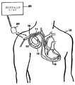
図1は、本発明に従って用いるようになっている埋め込み可能医療デバイス(IMD)システムの図である。図1に示す医療デバイスシステムは、患者12に埋め込まれた埋め込み可能デバイス10を含む。当技術分野の従来のやり方によれば、ペースメーカ10は、密閉された生物学的に不活性な外ケーシング内に収容され、外ケーシングは、それ自体、導電性であって、ペースメーカペーシング/検知回路の中性電極として機能することができる。1つまたは複数のペースメーカのリード線(図1において参照番号14でひとまとめで特定される)は、従来の方法で、ペースメーカ10に電気接続され、静脈18を介して患者の心臓16内に延びる。リード線14の遠位端の略近傍には、心臓電気信号を受け取るための、かつ/または、心臓16にペーシング電気刺激を送出するための1つまたは複数の露出した導電性電極が配設される。当業者には理解されるように、リード線14は、その遠位端(複数可)が心臓16の心房および/または心室内にある状態で埋め込まれることができる。
【0020】
本発明は、ペースメーカを含む実施形態において、本明細書で説明されるが、本開示の恩恵を受ける当業者は、本発明が、いくつかの他のタイプの埋め込み可能医療デバイスシステムと共に、また、実際に、2つの物理的に離れたコンポーネント間の通信リンクを設けることが望ましい任意の用途で実施することができることを理解するであろう。
【0021】
図1には、アップリンクおよびダウンリンク通信チャネルを介して埋め込みデバイス10と無侵襲通信を行う外部プログラミングユニット20も示す。これは以下でさらに詳細に説明する。埋め込みデバイス10とプログラマ20の間の双方向通信を容易にするために、従来の医療デバイスプログラミングシステムに従って、プログラミングユニット20には、プログラミングヘッド22が連結される。多くの既知の埋め込み可能デバイスシステムにおいて、図1に示すようなプログラミングヘッドは、当技術分野の一般的なやり方に従って、患者の体のデバイスの埋め込み部位の上に位置決めされ(通常、皮膚接触位置から2〜3インチ以内)、それによって、ヘッド内の1つまたは複数のアンテナは、埋め込みデバイスの密閉格納部内に配設されるか、または、デバイスのコネクタブロック内に配設されたアンテナに対してRF信号の送受信を行うことができる。
【0022】
図2は、現在開示している発明によるプログラミングユニット20の斜視図である。内部において、プログラマ20は処理ユニット20(図示せず)を含み、処理ユニットは、現在開示している発明によれば、パーソナルコンピュータタイプマザーボード、たとえば、Intel Pentium3マイクロプロセッサおよびデジタルメモリなどの関連回路要素を含むコンピュータマザーボードである。プログラマコンピュータシステムのデザインおよび動作の詳細は、本開示では詳細には述べられないであろう。その理由は、こうした詳細が、当業者にはよく知られていると考えられるためである。
【0023】
図2を参照すると、プログラマ20は外ハウジング60を備え、外ハウジングは、熱可塑性材料または適度に頑丈ではあるがそれでも比較的軽量の別の材料でできているのが好ましい。図2において、概して62で示す運搬ハンドルは、ハウジング60の前面に一体に形成される。ハンドル62を用いると、プログラマ20をブリーフケースのように運ぶことができる。
【0024】
関節式ディスプレイスクリーン64はハウジング60の上面に配設される。ディスプレイスクリーン64は、プログラマ20が使用されていない時に閉じた位置(図示せず)に折りたたんで閉じられ、それによって、プログラマ20のサイズが減り、プログラマの輸送および保管中におけるディスプレイ64の表示面が保護される。
【0025】
フロッピディスクドライブは、ハウジング60内に配設され、ディスク挿入スロット(図示せず)を介してアクセス可能である。ハードディスクドライブもまた、ハウジング60内に配設されており、ハードディスクドライブ作動インジケータ(たとえば、LED(図示せず))が、ハードディスク起動の可視表示を与えるために設けられるであろうことが予想される。
【0026】
当業者には理解されるように、患者の伝導系の状態を確定する手段を設けることが望ましいことがしばしばある。通常、プログラマ20は外部ECGリード線24を装備している。本発明によってこれらのリード線が不要になる。
【0027】
本発明によれば、プログラマ20は、内部プリンタ(図示せず)を装備しており、それによって、患者のECGまたはプログラマのディスプレイスクリーン64上に表示されたグラフィックのハードコピーを生成することができる。General Scanning Co.から入手可能なAR−100プリンタなどのいくつかのタイプのプリンタが知られており、市販されている。
【0028】
図2の斜視図において、プログラマ20は、関節式ディスプレイスクリーン64が、複数の可能な開いた位置のうちの1つに持ち上げられており、それによって、プログラマ20のディスプレイエリアが、プログラマ20の前にいるユーザに見える。関節式ディスプレイスクリーンは、たとえば、陰極線管(CRT)または同様なものと比較すると比較的薄いことが特徴である、LCDまたはエレクトロルミネッセンスタイプであることが好ましい。
【0029】
当業者には理解されるように、ディスプレイスクリーン64は、ハウジング60内に配設されたコンピュータ回路要素に動作可能に結合し、内部コンピュータの制御下で、グラフィックおよび/またはデータの可視表示を行うようになっている。
【0030】
図2を参照して本明細書で述べるプログラマ20は、Thomas J. Winklerに発行された「Portable Computer Apparatus With Articulating Display Panel」と題する米国特許第5,345,362号(その全体が参照により本明細書に援用される)にさらに詳細に記載されている。Medtronic Model 9790プログラマは、本発明が有利に実施されることができる埋め込み可能デバイス−プログラミングユニットである。
【0031】
図3は、現在開示している発明によるパルス発生器10を構成する電子回路要素のブロック図である。図3からわかるように、ペースメーカ10は、デバイスのペーシング機能および検知機能を制御する主刺激制御回路21を備える。刺激制御回路21と連結する回路要素は、たとえば、Sivula他に発行された特許第5,052,388号「Method And Apparatus For Implementing Activity Sensing In A Pulse Generator」に開示されているものによれば、従来のデザインであってよい。パルス発生器10の一定の部品が、そのデザインおよび動作において従来型である限りにおいて、こうした部品は、本明細書では詳細に述べられないであろう。その理由は、こうした部品のデザインおよび実施態様は、当業者にとっては日常的な問題であると考えられるからである。たとえば、図3の刺激制御回路21は、検知増幅器回路要素25、刺激パルス出力回路要素26、水晶クロック28、ランダムアクセスメモリおよびリードオンリメモリ(RAM/ROM)ユニット30、および中央処理ユニット(CPU)32を含み、これらは全て当技術分野ではよく知られている。
【0032】
ペースメーカ10はまた、内部通信回路34を含み、それによって、図2においてより詳細に述べるように、外部プログラマ/制御ユニット20と通信することができる。
さらに図3を参照すると、パルス発生器10は、1つまたは複数のリード線14に結合し、リード線は、埋め込み時に、図1を参照して先に述べたように、パルス発生器10の埋め込み部位と患者の心臓16の間で横方向に延びる。物理的には、リード線14とパルス発生器10の種々の内部部品の間の接続部は、図1に示す従来のコネクタブロック組み立て品11によって補助される。当業者にはよく知られているように、電気的には、リード線の導体とパルス発生器10の内部電気部品の結合は、リード線インタフェース回路19によって補助されることができ、リード線インタフェース回路は、マルチプレクサがするように機能して、たとえば、心房チップ/リング電極導体ATIP/ARINGおよび心室チップ/リング電極導体VTIP/VRINGを含むリード線14の種々の導体と、パルス発生器10の個々の電気部品の間に、選択的にかつ動的に、必要とする接続を確立するようにする。明確にするために、リード線14とパルス発生器10の種々の部品の間における特定の接続部を図3には示していないが、たとえば、リード線14は、一般的なやり方に従って、必ず、検知増幅器回路要素25および刺激パルス出力回路26に直接的に、または間接的に結合し、それによって、心臓電気信号は、検知回路要素25に送られ、刺激パルスは、リード線14を介して心臓組織に送出されることができることが、当業者には明らかとなろう。図3には、一般に、埋め込みデバイスに含まれて、たとえば、デバイスの検知回路要素を高電圧刺激パルスから保護する保護回路要素も示されていない。
【0033】
先に述べたように、刺激制御回路21は中央処理ユニット32を含み、中央処理ユニットは、既製のプログラム可能マイクロプロセッサまたはマイクロコントローラであってよいが、本発明ではカスタム集積回路である。CPU32と刺激制御回路21の他の部品の間の特定の接続部が図3には示されていないが、CPU32が、RAM/ROMユニット30に格納したプログラムの制御下で、刺激パルス出力回路26および検知増幅器回路25のタイミングを合わせた動作を制御するように働くことは当業者には明らかになるであろう。当業者は、こうした動作機構をよく知っていると考えられる。
【0034】
続けて図3を参照すると、水晶発振器回路28、目下のところ好ましい実施形態では、32,768Hz水晶制御発振器は、主タイミングクロック信号を刺激制御回路21に供給する。再び、こうしたクロック供給信号が、タイミング合わせされるパルス発生器10の種々の部品に供給されるラインは、明確にするために、図3から省略される。
【0035】
図3に示すパルス発生器10の種々の部品は、当技術分野の一般的なやり方に従って、ペースメーカ10の密閉格納部内に収容されたバッテリ(図示せず)によって駆動される。図面を明確にするために、バッテリおよびバッテリとパルス発生器10の他の部品の間の接続部は示していない。
【0036】
CPU32が発する信号の制御下で心臓刺激を生成するように働く、刺激パルス出力回路26は、たとえば、Thompsonに発行された「Body Stimulator Output Circuit」と題する米国特許第4,476,868号(その全体が参照により本明細書に援用される)に開示されているタイプのものであってよい。しかし、再び、当業者は、本発明を実施する目的に適しているであろう、多くの種々のタイプの従来技術のペーシング出力回路の中から選択できるであろうことが考えられる。
【0037】
従来のデザインである検知増幅器回路25は、リード線14から心臓電気信号を受け取り、こうした信号を処理して、心房収縮(P波)および心室収縮(R波)を含む、特定の心臓電気事象の発生を反映する事象信号を導出するように働く。CPUは、当技術分野の一般的なやり方に従って、パルス発生器10の同期した刺激動作を制御する時に用いるために、これらの事象指示信号をCPU32に供給する。さらに、これらの事象指示信号は、医師または臨床医に対する可視表示のために、アップリンク送信によって外部プログラミングユニット20に伝達されることができる。
【0038】
当業者は、ペースメーカ10が、いくつかの他の部品およびサブシステム、たとえば、活動センサおよび関連回路要素を含んでよいことを理解するであろう。しかし、ペースメーカ10のこうした付加的な部品が有るか無いかは、本発明に関係しないと考えられ、有るか無いかは、主に、ペースメーカ10内の通信サブシステム34および外部ユニット20内の関連通信サブシステムの実施態様および動作に関係する。
【0039】
図4は、本発明が実施されることができる埋め込んだペースメーカ10の断面図である。ペースメーカ10の主要部品は、電子回路要素52および密閉電源50が収容された密閉ケーシンングを含む。リード線コネクタモジュール11は、ペースメーカ10の心房リード線および心室リード線の近位端が開口15を通して挿入されることができる格納部を提供する。リード線コネクタモジュール11は、ペースメーカケーシング10に接続され、当技術分野ではよく知られているように、リード線コネクタと密閉フィードスルー(図示せず)の間に電気接続部(同じく図示せず)を含む。
【0040】
さらに図4を参照すると、フィードスルー/電極組み立て品54は、ペースメーカケーシングのほぼまたは実質的に平らな周縁部上の場所に溶接される。好ましい実施形態において、本発明において開示されたようなフィードスルー/電極組み立て品の設置を受け入れる、まるい端部を含む少し平らな斜視形状を有するペースメーカの完全な周縁部を製造することができる。これらのフィードスルー/電極組み立て品54は、一体密閉性(integral hermiticity)のためにペースメーカケーシングに溶接され、アクセスを得るための個別のフィードスルー56を通って、ワイヤ55によって電子回路要素52に接続される。
【0041】
図5は、ECG検知電極と組み合わせた、本発明の第1の実施形態の代替構造のいくつかの断面図である。この実施形態において、完全な組み立て品は、実に小さく、ペースメーカケーシングと適合するようにデザインされている。完全な組み立て品のサイズが小さいため、検知電極は、P波などの弱い/非常にわずかな心臓脱分極波を検出することができる材料からデザインされ、製造されねばならない。
【0042】
さらに、以下の図6〜図12で開示するものを含む皮下電極組み立て品は、密閉性があり(10−6ccHe/秒未満で、好ましくは10−9ccHe/秒)、生体適合性があり、ペースメーカケーシングに結合可能か、または、完全に一体にできなければならない。概して、本明細書で開示した電極は全て以下の材料から構成されることができる。絶縁体は、ガラス、セラミック(直接ろう付け)、高分子、またはガラスセラミックから成ってよい。フェルールは、チタン、ニオブ、ステンレススチールなどの任意の適当な合金または金属、またはこれらの金属と合金の組み合わせから作製されてよい。フィードスルー導体は、ニオブ、タンタル、プラチナ、またはプラチナ−イリジウムなどの任意の適当な合金でできていてよい。検知電極は、プラチナ、プラチナブラック、チタン、窒化チタン、または酸化ルテニウムなどの任意の適当な材料またはそれらの組み合わせで構成されてよい。焼結(粉末冶金)、スパッタリング、めっき、CVD、PVD、または他の方法を含む、電極コーティング堆積法を用いて、大きな表面積および低い分極を得ることができる。イオンエッチング、方向性凝固(directional solidification)、または他のプロセスを用いて、表面にきめを出して、電極の表面積を増やし、製造容易性を単純にすることができる。
【0043】
図5Aおよび図5Bは、単純な皮下ECG電極組み立て品を示す。図5Aは、ペースメーカケーシング(図示せず)のフェルール73への溶接を受け入れる、任意選択の溶接用ノッチ70を有するフェルール73に取り付けられたフィードスルー導体75を示す。ガラス絶縁体85は、フィードスルー導体75およびフェルール73に接合する。好ましくは、フィードスルー導体75は、機械加工されて、ECG検知電極として働く。2000年12月13日に出願されたGuck他によるP−8787「Thin Film Electrodes for Sensing Cardiac Depolarization Signals」第09/736,046号は、フィードスルー導体をECG電極に変換する製造プロセスを開示した。図5Bは、絶縁体76およびフェルール73によって支持された導体75を有する、ろう付けされたフィードスルー84を示す。これらの部品は金ろう77と接合される。
【0044】
図5Aおよび図5Bに示す実施形態は、エレガントな電極デザインおよび背が低いことを開示している。実施形態は、目立った突起がなく、したがって、埋め込み手技をより容易にし、患者に対する快適さを増すのに適している。
【0045】
図6は、大きな表面積を有するECG検知電極を利用する、本発明の第2の実施形態についての4つの図を示す。図6Aは断面図、図6Bは平面図、図6Cは斜視図、および図6Dは断面図であり、それらの全ては、とりわけ、改良したフェルールケーシング内のガラス絶縁体を示す。
【0046】
図6Aを参照すると、ほぼ平らな端部を持つ電極74で終端するフェルール導体75の断面図が示される。電極74は、フェルール73内の凹所に置かれて、フェルールは、任意選択の溶接用ノッチ70でペースメーカケーシングに溶接されている。したがって、完全な組み立て品は、ペースメーカケーシングの上または外に突き出る部品がない。フィードスルー導体75は、絶縁体76の開口に嵌挿され、絶縁体には、フィードスルー導体が、ろう77によって接合される。絶縁体76は、ECG信号が、ペースメーカ10内のSEA回路要素に電気接続されているフィードスルー導体75を通って、検知電極74から巡回する時、ECG信号の電気的絶縁を維持する。ろう77は、組み立て品を密閉し、電極74のまわりの空洞を満たす体液の侵入を防ぐのに役立つ。
【0047】
この実施形態において、ECG検知電極74の増加した表面積は、本発明の大きな特徴の1つである。幾何学的な表面積が増えて、より小さな振幅を有する心臓波形、たとえば心房細動波の検出が改善される。さらに、幾何学的な表面積が増えることは、ECG検知電極で、またはECG電極のまわりでの分極効果を減衰させることができる。両方の特徴は、ECG波形の適切な検出の確保に役立つ。構造は、心臓脱分極信号の適当な検出および送信を可能にする。代替の実施形態において、電極コーティングを用いて、より大きな表面積を得、低分極をもたらすことができる。コーティング堆積法は、焼結(粉末冶金)、スパッタリング、めっき、CVD、PVD、または他の方法を含んでよい。さらに、イオンエッチング、方向性凝固、または他のプロセスを用いて、表面にきめを出して、電極の表面積を増やし、製造容易性を単純にすることができる。
【0048】
検知電極74は、フィードスルー導体75と一体でかつ均質であり、焼結、スパッタリング、めっきなどのような堆積法によって作製されることができる。別法として、検知電極74は、後で、形状記憶合金、溶接、ろう付け、圧縮干渉接合などによって、フィードスルー導体に取り付けられてよい。
【0049】
図6Dは、同じフィードスルー導体75および検知電極74が用いられている実施形態の断面図である。ただし、以下の点を除く。すなわち、1)フィードスルー導体/電極をフェルールと接合するため、2)電気的に絶縁して、信号の完全性を維持するため、および3)組み立て品を密閉するために、ガラス85が用いられる。
【0050】
図7は、背の低いECG検知電極およびフィルタ(すなわち、コンデンサ)を利用する、本発明の第3の実施形態についての4つの図を示す。
図7Aは、多層セラミックコンデンサ71を付加したものを示しており、多層セラミックコンデンサは、電磁干渉をろ過して、信号をペースメーカ回路要素に伝える前に検出信号を改善するのに役立つ。フィードスルー導体およびフィードスルーフェルールは、コンデンサに電気的に結合される。コンデンサ71は、組み立て品内に設置され、非導電性エポキシ79を用いて固定されることができる。導電性エポキシ78を用いて、コンデンサ71をフィードスルー導体75に結合することができる。図7Dにおいて、フィルタコンデンサ71はガラス絶縁体85と共に用いられることにも留意されたい。
【0051】
図8は、大きな表面積を有するECG検知電極およびコンデンサの両方を利用する、本発明のさらに別の実施形態についての4つの図を示す。図8Aにおいて、ECG検知電極74は、図6に関して開示した方法、すなわち、第2の実施形態と同じ方法で実施される。大きな表面積を有する検知電極を用いる理由は、図6で挙げた理由と同じである。
【0052】
図9は、本発明の第3および第4の実施形態(図7および図8)が、ポリイミドディスクと組み立てられて、組み立て品が漏れ試験できるようになる方法についての3つの図を示す。この図は、密閉性を試験するための、すなわち、組み立て品が漏れを試験され得るかを判断するための重要要素に的を絞っている。コンデンサ71の直下にポリイミドディスク72を付加することによって、この目的が達成される。漏れ試験可能なフィードスルーをさらに説明するために、2000年10月25日に出願された、Fraley他によるP−8990「Leak Testable Capacitive Filtered Feedthrough for an Implantable Medical Device」第09/696,601号(その全体が参照により本明細書に援用される)が参照される。先に開示した実施形態と同様に、絶縁体としてガラス(図示せず)を用いて、同じ要素が組み立て品に付加されるであろう。
【0053】
図10は、背が低く、大きな表面積のディスク電極80を有する、本発明の断面図を示す。具体的に、電極80は、図6および図8で開示した実施形態で実施されて、ECG検知電極の表面積をさらに増やすようにすることができる。電極は、フィードスルーをシールドに溶接した後、フィードスルー導体に取り付けられる。電極の取り付けは、レーザ溶接、抵抗スポット溶接、機械的干渉、または他の等価な方法によって行われることができる。
【0054】
図11は、先に開示した実施形態において示した組み立て品と共に用いることができる種々の電極タイプの図である。図11Aは、(図6に示すように)検知電極86が取り付けられている、標準的な、頭がほぼ平らのフィードスルー導体である。図11Bおよび図11Cに示すように、電極の代替のタイプを用いることができる。フィードスルー導体75を、白金粉末室67を含むように改造することができる。図11Bの電極75は、Pt粉末68でコーティングされ、焼結される。図11Cの電極75は、Pt粉末68およびPt黒69でコーティングされ、焼結される。本発明によれば、焼結したPt68およびPt黒69の任意の組み合わせを用いることができる。図11Dに示すように、全ての電極はステロイドプラグ82を含んでよい。図11Eおよび図11Fは、本発明による製造ステージを示す。具体的には、図11Fに示すように、電極75は、電極ディスク80を貫通する。図11Eに示すように、突出部は、従順な輪郭を有するように、レーザ溶接されるか、機械的に成形されるのが好ましい。フィードスルー導体は、背の低い電極ディスク80を貫挿する。図11Fに点線で示すように、フィードスルー導体は、ディスク80を貫通し、図11Eに示すように、電極75をフィードスルー導体に取り付けるために溶接される。
【0055】
図12Aおよび図12Bは、形状記憶合金66を利用して、より容易でかつより低コストの作製を可能にする組み立て品の例である。図12Aは、検知電極74をフェルール73およびペースメーカケーシング(図示せず)から電気的に絶縁するための別の材料の絶縁体87を伴った、セラミックまたはガラス絶縁体83の実施態様を示す。図12Bの電極は、エポキシバックフィル79および背の低い検知電極80をフェルール73およびペースメーカケーシングから電気的に絶縁するための絶縁体88を用いる代替の実施形態である。
【0056】
上記の特定の実施形態は本発明の実施を例示する。したがって、本発明または添付請求項の範囲から逸脱することなく、当業者に知られているか、または本明細書で開示された他の手段を使用することができることが理解されるべきである。したがって、本発明は、本発明の範囲から逸脱することなく、具体的に述べられた以外の方法で実施することができることが理解されるべきである。全ての要素に関して、その要素を、無数の等価な代替物で置き換えることができ、代替物のうちのいくつかのみが本明細書で開示されている。
【図面の簡単な説明】
【0057】
【図1】患者に埋め込んだ密閉デバイスおよび外部プログラミングユニットを含む、本発明による体に埋め込み可能なデバイスシステムの図である。
【図2】図1の外部プログラミングユニットの斜視図である。
【図3】図1の埋め込みデバイスのブロック図である。
【図4】本発明を好ましい実施形態として実施することができる埋め込んだペースメーカの断面図である。
【図5】単純なECG検知電極を用いた、本発明の第1の実施形態のいくつかの代替の作製のうちの2つの断面図である。
【図6】大きな表面積を有するECG検知電極を利用する、本発明の第2の実施形態の4つの図である。
【図7】背が低く、ろ過用コンデンサを有するECG検知電極を利用する、本発明の第3の実施形態の4つの図である。
【図8】大きな表面積およびろ過用コンデンサを有するECG検知電極を利用する、本発明の第4の実施形態の4つの図である。
【図9】本発明の第3および第4の実施形態(図7および図8)を、ポリイミドディスクを用いて組み立て、組み立て品を漏れ試験可能にする方法についての4つの図である。
【図10】背の低いディスク電極を有する、本発明の断面図である。
【図11】先の図で示した組み立て品において用いることができる種々の電極タイプの図である。
【図12】形状記憶合金を用いてフィードスルー導体に取り付けられた電極の断面図である。【Technical field】
[0001]
The present invention relates generally to implantable pacemakers, and more particularly, to a subcutaneous electrode implemented to sense, acquire, and store electrocardiographic data and waveform traces from an implanted pacemaker. More particularly, the present invention relates to various embodiments that include the manufacture and assembly of such electrodes with feedthroughs that facilitate electrical connection to pacemaker circuitry.
[Background Art]
[0002]
Electrocardiogram (ECG) signals are commonly used in medicine to determine the state of the electrical conduction system of a human heart. As practiced, an ECG recording device is typically attached to a patient by ECG leads connected to skin electrodes arranged on the patient's body to provide any one of 12 possible vectors. A record is obtained which represents the cardiac waveform of one vector.
[0003]
Since the first implantation of a cardiac pacemaker, the development of sophisticated and programmable cardiac pacemakers and pacemaker-cardioverter-defibrillator (PCD) arrhythmia control devices designed to detect arrhythmias and provide appropriate therapy With this, implantable IMD technology has advanced. Detection of various arrhythmic episodes and discrimination between arrhythmic episodes to cause the delivery of appropriate therapy is of great interest. Implant prescription and implantation device programming is based on analysis of the PQRST electrocardiogram (ECG) and electrogram (EGM). For such analyses, the waveforms are typically separated into P and R waves of the system, and the P and R waves are believed to detect atrial and ventricular depolarizations, respectively. Such a system detects the occurrence of P and R waves in the heart, the rate of repetition of the P and R waves, regularity, the onset of rate fluctuations, the morphology of the P and R waves, and the P and R waves. It employs analyzing the propagation direction of the depolarization represented by the wave. Detecting, analyzing, and storing such EGM data within an implanted medical device is well known in the art. On the other hand, collection and use of the ECG trace (s) has generally been limited to the use of external ECG recording equipment attached to the patient by one sort or another type of surface electrode.
[0004]
The previously described ECG system using PQRST complex detection and analysis uses an externally attached electrode near or around the heart that can be used to detect or detect a cardiac depolarization wavefront. All depend on the spatial arrangement direction and the number.
[0005]
As the functionality and sophistication of implantable medical device systems have grown over the years, such systems have provided a means of communication between implanted and / or external devices, such as programming consoles, monitoring systems, and similar systems. It became necessary to include. For diagnostic purposes, the implanted device should be able to convey information to the physician or clinician regarding the operating status of the device and the condition of the patient. Transmit or telemeter digitized electrical signals indicative of cardiac electrical activity (eg, ECG, EGM, or the like) to obtain modern implantable devices that can be stored and / or analyzed by external devices It is possible.
[0006]
To diagnose and measure cardiac events, cardiologists have several tools to choose from. Such tools include 12-lead electrocardiograms, exercise stress electrocardiograms, Holter monitoring, radioisotope imaging, coronary angiography, myocardial biopsies, and blood serum enzyme tests. Despite these advances in the medical device field, surface ECGs have and have been a standard diagnostic tool since the very beginning of pacing. A 12-lead electrocardiogram (ECG) is generally the first procedure used to determine the condition of the heart before implanting a pacing system. The physician will then check the effectiveness of the pacemaker after implantation, usually using the ECG available through a programmer or extracorporeal telemetry transmission. The previous ECG trace is added to the patient's record and later used when comparing against recent traces. However, it should be noted that current art practice in ECG recording (either directly to an ECG recording device or to a pacemaker programmer) involves the use of external ECG electrodes and leads. .
[0007]
Unfortunately, surface ECG electrodes have technical disadvantages. For example, ECG analysis performed with existing external or body surface ECG systems may be limited by mechanical problems and poor signal quality. Electrodes mounted outside the body are a major source of signal quality problems and errors. This is because electrodes mounted outside the body are susceptible to interference such as, for example, muscle noise, electromagnetic interference, high frequency communication equipment interference, and baseline shift due to breathing. Signal degradation is also caused by contact problems, ECG waveform artifacts, and patient discomfort. Externally mounted electrodes are also subject to movement artifacts due to changes in position and relative displacement between the skin and the electrodes. In addition, external electrodes require special skin treatments, such as the application of electrolyte ointments or creams, to ensure proper electrical contact. Such a process involving positioning the electrodes and attaching ECG leads to the electrodes unnecessarily prolongs the pacemaker tracking session. One possible approach is to provide an implanted pacemaker with a trace that detects cardiac signals and is the same or comparable to the traces that can be obtained via ECG leads attached to surface (skin) electrodes. And a mechanism for converting a heart signal.
[0008]
Monitoring the electrical activity of the human heart for diagnostic and related medical purposes is well known in the art. For example, U.S. Pat. No. 4,023,565 issued to Ohlsson describes circuitry for recording ECG signals from multiple lead inputs. Similarly, U.S. Pat. No. 4,263,919 issued to Levin, U.S. Pat. No. 4,170,227 issued to Feldman et al., And U.S. Pat. No. 4,593,702 issued to Kepski et al. Describes a multi-electrode system that combines surface EKG signals to eliminate artifacts.
[0009]
The primary use of the multi-electrode system in the prior art is thought to be a vector electrocardiograph from ECG signals obtained from multiple electrodes in the chest and limbs. This is a technique for monitoring the direction of cardiac depolarization, including the amplitude of the cardiac depolarization wave. U.S. Pat. No. 4,121,576 issued to Greensite discloses such a system.
[0010]
Several body surface ECG monitoring electrode systems have been implemented in the past to detect ECG and perform vector electrocardiography studies. For example, U.S. Pat. No. 4,082,086 issued to Page et al. Discloses that a patient's skin may be used both for convenience and to ensure the correct orientation of one electrode relative to the other. A four-electrode orthogonal array that can be affixed is disclosed. U.S. Pat. No. 3,983,867 issued to Case discloses a six-axis display of voltage versus time ECG signals generated across a pair of sampled bipolar electrodes and ECG electrodes disposed on a patient at commonly used locations. 3 describes a vector electrocardiograph employing a reference system quadrature display.
[0011]
U.S. Patent No. 4,310,000 issued to Lindemans and U.S. Patent Nos. 4,729,376 and 4,674,508 issued to DeCote are hereby incorporated by reference. Discloses the use of a separate passive sensing reference electrode mounted on a pacemaker connector block or otherwise insulated from the pacemaker case. The passive electrode is not part of the stimulation reference electrode and is therefore implemented to provide a sensing reference electrode with no residual afterpotential at the surface following stimulation pulse delivery.
[0012]
Further, with respect to subcutaneously implanted EGM electrodes, the aforementioned Lindemans U.S. Pat. No. 4,310,000 discloses one or more reference sensing electrodes positioned on the surface of a pacemaker case, as described above. ing. In a related art, U.S. Pat. No. 4,313,443 issued to Lund describes a subcutaneous implanted electrode or electrode used during ECG monitoring.
[0013]
U.S. Patent No. 5,331,966 issued to Bennett, which is hereby incorporated by reference, discloses cardiac electrical signals generated by closely spaced subcutaneous electrode arrays (located on the implanted device body). Disclosed are methods and apparatus for providing enhanced functionality for detecting and collecting data.
[0014]
Most recently filed on Oct. 26, 2000, Ceballos et al., P-9033, "Surround Shroud Connector and Electrode Housings for a Subcutaneous Electrode Array and Leadless ECG's", 09 / 697,438, which is incorporated herein by reference in its entirety. Disclose an alternative method and apparatus for detecting cardiac electrical signals by means of a subcutaneous electrode array located on a circumferentially positioned shroud at the periphery of an implanted pacemaker. Related submissions: Bravec et al., P-9041, "Subcutaneous Electrode for Sensing Electrical Signals of the Heart," Ser. No. 09 / 703,152, filed Oct. 31, 2000, which is incorporated herein by reference in its entirety. Discloses the use of a spiral electrode implemented with a shroud described in P-9033. In addition, Guck et al., P-8786 "Multilayer Ceramic Electrodes for Sensing Cardiac Depolarization Signals", filed October 25, 2000, Ser. No. 09 / 696,365, and Puck filed December 13, 2000. -8787 "Thin Film Electrodes for Sensing Cardiac Depolarization Signals" 09 / 736,046, incorporated herein by reference in its entirety, was incorporated along and into the periphery of an implantable pacemaker. Disclosed is the use of multilayer ceramic and thin film ECG electrodes located in the recess.
[Summary of the Invention]
The present invention relates to various electrode designs that allow the electrodes to be incorporated directly into the feedthrough. Depending on the design, the feedthrough ferrules can be individually welded at desired locations around the perimeter of the implantable pacemaker, after which the feedthrough / electrodes can be made in existing ferrules. Alternatively, a complete feedthrough / electrode assembly can be made and then welded to the pacemaker as one piece. These feedthrough / electrode assemblies are electrically connected to circuitry of the implantable pacemaker and have no leads to detect cardiac depolarization waveforms that can be displayed as electrocardiographic traces on external devices that communicate with the pacemaker. A subcutaneous electrode array (SEA) is created. Once the programmer's programming head is positioned on the implanted device with the leadless SEA, the electrocardiograph trace waveform can be displayed and viewed on the programmer screen. These waveforms are also described in P-7683 "Leadless Fully Automatic Pacemaker Follow-Up" 09 / 749,169, filed December 27, 2000 by Combs and Berg, which is incorporated herein by reference in its entirety. ) Can be telemetered outside the body to an external device located near or at a distance to the patient.
[0015]
The present invention replaces, among other things, prior art external mounting electrodes and electrode wires currently used on leadless ECG implantable pacemakers described in US Pat. No. 5,331,966 issued to Bennett. there is a possibility. In general, prior art approaches include electrodes placed on the face of an implanted pacemaker. When facing muscles, the electrodes are more likely to detect myoelectric potential and are more susceptible to baseline drift. The present invention minimizes the detection of myoelectric potential, thereby making the pacemaker less sensitive to the orientation of the patient's incision pocket. Further, by allowing the device to be implanted on either side of the chest, it allows for maximum electrode separation and minimal signal variation. This is mainly because the arrangement direction of the pacemaker in the pocket fluctuates. Implantable device electrodes need to be placed on the periphery of the pacemaker to maximize the distance between the electrode pairs.
[0016]
The present invention relates to a surface mount as described in P-9033 "Surround Shroud Connector And Electrode Housings For A Subcutaneous Electrode Array And Leadless ECG's" 09 / 697,438 filed Oct. 26, 2000 by Ceballos et al. Eliminates the need for a compliant shroud that normally houses the electrodes and connecting wires. Since the feedthrough / electrode assembly is an integral functional element, the complete assembly can be welded directly into the IPG casing. The present invention, including the manufacturing process disclosed herein, eliminates the need for a compliant siroud in addition to the structural efficiency and ease of operation of an implantable pacemaker during an implantation procedure.
[0017]
The electrode spacing in the present invention allows for maximum electrode spacing, minimum myoelectric electrical noise, and at the same time adequate insulation from the pacemaker casing, especially for welding the assembly to the pacemaker casing. The electrode spacing around the periphery of the pacemaker preferably maintains a maximum and is equidistant between electrode pairs. Spacing, as disclosed for the three equally spaced embodiment, maintains the maximum average signal. As shown using a mathematical model, this arrangement is preferred because the spacing of the three vectors between the electrode pairs is equal and the angles between the vectors are equal. Such an arrangement of electrode pairs also minimizes signal variations. An alternative three-electrode embodiment includes electrodes arranged such that the two vectors are equally spaced and the angle between the vectors is set to 90 °. The combination of the vectors of these embodiments allows for proper sensing of the cardiac signal (ECG). Another disclosure of the location of three and four electrodes in a subcutaneous electrode array (SEA) is described in P-8552, "Subcutaneous Electrode Array Virtual ECG Lead" 09/721, filed Nov. 22, 2000 by Panken and Reinke. No. 275, which is hereby incorporated by reference in its entirety.
[0018]
Similar to the use of compliant shrouds, spiral electrodes, and multilayer ceramic electrodes, the present invention allows a physician or medical technician to perform a lead-free follow-up, which in turn involves an external lead. Eliminate the time it takes to attach the line to the patient. These time savings reduce the cost of follow-up and allow physicians or medical technicians to look at more patients. Other embodiments include, but are not limited to, Holter monitoring with event storage, arrhythmia detection and monitoring, capture detection, ischemia detection and monitoring (ST elevation and suppression on ECG, QT interval changes) And telephone transmission and telemetry monitoring.
BEST MODE FOR CARRYING OUT THE INVENTION
[0019]
FIG. 1 is an illustration of an implantable medical device (IMD) system adapted for use in accordance with the present invention. The medical device system shown in FIG. 1 includes an
[0020]
Although the present invention is described herein in embodiments that include a pacemaker, those of ordinary skill in the art having the benefit of this disclosure will appreciate that the present invention can be used with several other types of implantable medical device systems, and Indeed, it will be appreciated that it may be implemented in any application where it is desirable to provide a communication link between two physically separated components.
[0021]
FIG. 1 also shows an
[0022]
FIG. 2 is a perspective view of a
[0023]
Referring to FIG. 2, the
[0024]
The articulated display screen 64 is disposed on the upper surface of the housing 60. The display screen 64 is folded and closed in a closed position (not shown) when the
[0025]
The floppy disk drive is located within housing 60 and is accessible via a disk insertion slot (not shown). It is envisioned that a hard disk drive is also disposed within the housing 60 and a hard disk drive activity indicator (eg, an LED (not shown)) will be provided to provide a visual indication of hard disk startup. .
[0026]
As will be appreciated by those skilled in the art, it is often desirable to provide a means for determining the condition of the patient's conduction system. Typically,
[0027]
In accordance with the present invention, the
[0028]
In the perspective view of FIG. 2, the
[0029]
As will be appreciated by those skilled in the art, display screen 64 is operatively coupled to computer circuitry disposed within housing 60 to provide a visual display of graphics and / or data under the control of an internal computer. It has become.
[0030]
[0031]
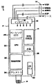
FIG. 3 is a block diagram of electronic circuit elements constituting the
[0032]
Still referring to FIG. 3, the
[0033]
As mentioned above, the
[0034]
With continued reference to FIG. 3, the
[0035]
The various components of the
[0036]
Stimulation pulse output circuit 26, which serves to generate cardiac stimulation under the control of the signals emitted by
[0037]
A
[0038]
Those skilled in the art will appreciate that
[0039]
FIG. 4 is a cross-sectional view of an implanted
[0040]
Still referring to FIG. 4, the feedthrough / electrode assembly 54 is welded to a location on a substantially or substantially flat periphery of the pacemaker casing. In a preferred embodiment, the complete perimeter of a pacemaker can be manufactured having a slightly flat perspective shape including a rounded end to accommodate the installation of a feedthrough / electrode assembly as disclosed in the present invention. These feedthrough / electrode assemblies 54 are welded to the pacemaker casing for integral hermiticity and connected to the electronics 52 by wires 55 through separate feedthroughs 56 to gain access. Is done.
[0041]
FIG. 5 is a cross-sectional view of some of the alternative structures of the first embodiment of the present invention in combination with ECG sensing electrodes. In this embodiment, the complete assembly is quite small and designed to fit the pacemaker casing. Due to the small size of the complete assembly, the sensing electrodes must be designed and manufactured from materials that can detect weak / very slight cardiac depolarization waves, such as P-waves.
[0042]
Further, subcutaneous electrode assemblies, including those disclosed in FIGS. 6-12 below, are hermetically sealed (10 -6 less than ccHe / sec, preferably 10 -9 ccHe / sec), must be biocompatible, coupleable to a pacemaker casing, or be completely integral. Generally, all of the electrodes disclosed herein can be comprised of the following materials: The insulator may consist of glass, ceramic (direct brazing), polymer, or glass ceramic. The ferrule may be made from any suitable alloy or metal, such as titanium, niobium, stainless steel, or a combination of these metals and alloys. The feedthrough conductor may be made of any suitable alloy, such as niobium, tantalum, platinum, or platinum-iridium. The sensing electrode may be comprised of any suitable material, such as platinum, platinum black, titanium, titanium nitride, or ruthenium oxide, or a combination thereof. Large surface areas and low polarization can be obtained using electrode coating deposition methods, including sintering (powder metallurgy), sputtering, plating, CVD, PVD, or other methods. Surfaces can be textured using ion etching, directional solidification, or other processes to increase the surface area of the electrodes and simplify manufacturability.
[0043]
5A and 5B show a simple subcutaneous ECG electrode assembly. FIG. 5A shows a feedthrough conductor 75 attached to a ferrule 73 having an optional welding notch 70 that receives a weld to a ferrule 73 of a pacemaker casing (not shown). The glass insulator 85 is joined to the feed-through conductor 75 and the ferrule 73. Preferably, feedthrough conductor 75 is machined to serve as an ECG sensing electrode. P-8787 "Thin Film Electrodes for Sensing Cardiac Depolarization Signals", Ser. No. 09 / 736,046, filed Dec. 13, 2000 by Guck et al., Disclosed a manufacturing process for converting feedthrough conductors to ECG electrodes. FIG. 5B shows a brazed feedthrough 84 having a conductor 75 supported by an insulator 76 and a ferrule 73. These parts are joined with the brazing solder 77.
[0044]
The embodiment shown in FIGS. 5A and 5B discloses an elegant electrode design and low profile. Embodiments have no prominent protrusions and are therefore suitable for making the implantation procedure easier and increasing patient comfort.
[0045]
FIG. 6 shows four views for a second embodiment of the present invention utilizing an ECG sensing electrode having a large surface area. 6A is a cross-sectional view, FIG. 6B is a plan view, FIG. 6C is a perspective view, and FIG. 6D is a cross-sectional view, all of which show, inter alia, a glass insulator in a modified ferrule casing.
[0046]
Referring to FIG. 6A, a cross-sectional view of a ferrule conductor 75 terminating at an electrode 74 having a substantially flat end is shown. The electrode 74 is placed in a recess in the ferrule 73, and the ferrule is welded to the pacemaker casing with an optional welding notch 70. Thus, the complete assembly has no parts protruding above or outside the pacemaker casing. The feed-through conductor 75 is inserted into an opening of the insulator 76, and the feed-through conductor is joined to the insulator by a solder 77. Insulator 76 maintains electrical isolation of the ECG signal as it circulates from sensing electrode 74 through feedthrough conductor 75 which is electrically connected to the SEA circuitry in
[0047]
In this embodiment, the increased surface area of the ECG sensing electrode 74 is one of the major features of the present invention. The increased geometric surface area improves the detection of cardiac waveforms having smaller amplitudes, such as atrial fibrillation waves. In addition, the increased geometric surface area can attenuate polarization effects at or around the ECG sensing electrode. Both features help ensure proper detection of the ECG waveform. The structure allows for proper detection and transmission of the cardiac depolarization signal. In an alternative embodiment, an electrode coating can be used to obtain a larger surface area and provide a lower polarization. Coating deposition methods may include sintering (powder metallurgy), sputtering, plating, CVD, PVD, or other methods. In addition, the surface can be textured using ion etching, directional solidification, or other processes to increase the surface area of the electrode and simplify manufacturability.
[0048]
The sensing electrode 74 is integral and homogeneous with the feedthrough conductor 75, and can be made by a deposition method such as sintering, sputtering, plating, and the like. Alternatively, sensing electrode 74 may be later attached to the feedthrough conductor by shape memory alloy, welding, brazing, compression interference bonding, or the like.
[0049]
FIG. 6D is a cross-sectional view of an embodiment in which the same feedthrough conductor 75 and sensing electrode 74 are used. However, the following points are excluded. Glass 85 is used for 1) joining the feedthrough conductor / electrode to the ferrule, 2) electrically insulating and maintaining signal integrity, and 3) sealing the assembly. .
[0050]
FIG. 7 shows four views for a third embodiment of the present invention utilizing a short ECG sensing electrode and a filter (ie, a capacitor).
FIG. 7A shows the addition of a multilayer ceramic capacitor 71, which filters out electromagnetic interference and helps to improve the detection signal before transmitting the signal to pacemaker circuitry. The feedthrough conductor and the feedthrough ferrule are electrically coupled to the capacitor. Capacitor 71 can be installed in the assembly and secured using a non-conductive epoxy 79. Capacitor 71 can be coupled to feedthrough conductor 75 using conductive epoxy 78. It should also be noted that in FIG. 7D, the filter capacitor 71 is used with a glass insulator 85.
[0051]
FIG. 8 shows four views for yet another embodiment of the present invention utilizing both an ECG sensing electrode and a capacitor having a large surface area. 8A, the ECG sensing electrode 74 is implemented in the manner disclosed with respect to FIG. 6, ie, in the same manner as in the second embodiment. The reason for using the sensing electrode having a large surface area is the same as the reason given in FIG.
[0052]
FIG. 9 shows three views of how the third and fourth embodiments of the present invention (FIGS. 7 and 8) are assembled with a polyimide disc so that the assembly can be leak tested. This figure focuses on the key factors for testing hermeticity, ie, determining whether an assembly can be tested for leaks. This object is achieved by adding a polyimide disk 72 directly below the capacitor 71. To further illustrate leak testable feedthroughs, P-8990 "Leak Testable Capacitive Filtered Feedthrough for an Implantable Medical Device", 09 / 696,601, filed October 25, 2000, by Fraley et al. Which is hereby incorporated by reference in its entirety). As with the previously disclosed embodiments, the same components would be added to the assembly using glass (not shown) as the insulator.
[0053]
FIG. 10 shows a cross-sectional view of the present invention with a short, large surface area disk electrode 80. Specifically, electrode 80 can be implemented in the embodiments disclosed in FIGS. 6 and 8 to further increase the surface area of the ECG sensing electrode. The electrodes are attached to the feedthrough conductor after welding the feedthrough to the shield. The mounting of the electrodes can be performed by laser welding, resistance spot welding, mechanical interference, or other equivalent methods.
[0054]
FIG. 11 is an illustration of various electrode types that can be used with the assemblies shown in the previously disclosed embodiments. FIG. 11A is a standard, substantially flat-headed feedthrough conductor to which the sensing electrode 86 is attached (as shown in FIG. 6). As shown in FIGS. 11B and 11C, alternative types of electrodes can be used. The feedthrough conductor 75 can be modified to include a platinum powder chamber 67. 11B is coated with Pt powder 68 and sintered. 11C is coated with Pt powder 68 and Pt black 69 and sintered. According to the present invention, any combination of sintered Pt 68 and Pt black 69 can be used. All electrodes may include a steroid plug 82, as shown in FIG. 11D. 11E and 11F show a production stage according to the invention. Specifically, as shown in FIG. 11F, the electrode 75 penetrates the electrode disk 80. As shown in FIG. 11E, the protrusions are preferably laser welded or mechanically shaped to have a compliant profile. The feedthrough conductor extends through the short electrode disk 80. 11F, the feedthrough conductor penetrates through the disk 80 and is welded to attach the electrode 75 to the feedthrough conductor, as shown in FIG. 11E.
[0055]
12A and 12B are examples of assemblies that utilize shape memory alloy 66 to allow easier and lower cost fabrication. FIG. 12A shows an embodiment of a ceramic or glass insulator 83 with an insulator 87 of another material for electrically insulating the sensing electrode 74 from the ferrule 73 and the pacemaker casing (not shown). The electrode of FIG. 12B is an alternative embodiment that uses an insulator 88 to electrically insulate the epoxy backfill 79 and the short sensing electrode 80 from the ferrule 73 and the pacemaker casing.
[0056]
The above specific embodiments illustrate the practice of the present invention. Therefore, it should be understood that other means known to those of skill in the art or disclosed herein can be used without departing from the scope of the invention or the appended claims. Therefore, it should be understood that the invention can be practiced otherwise than as specifically described without departing from the scope of the invention. For every element, that element can be replaced with a myriad of equivalent alternatives, only some of which are disclosed herein.
[Brief description of the drawings]
[0057]
FIG. 1 is a diagram of a body implantable device system according to the present invention, including a sealing device and an external programming unit implanted in a patient.
FIG. 2 is a perspective view of the external programming unit of FIG. 1;
FIG. 3 is a block diagram of the embedded device of FIG. 1;
FIG. 4 is a cross-sectional view of an implanted pacemaker in which the present invention may be implemented as a preferred embodiment.
FIG. 5 is a cross-sectional view of two of several alternative fabrications of the first embodiment of the present invention using a simple ECG sensing electrode.
FIG. 6 is four views of a second embodiment of the present invention utilizing an ECG sensing electrode having a large surface area.
FIG. 7 is four views of a third embodiment of the present invention utilizing an ECG sensing electrode that is short and has a filtering capacitor.
FIG. 8 is four views of a fourth embodiment of the present invention utilizing an ECG sensing electrode having a large surface area and a filtering capacitor.
FIGS. 9A and 9B are four views of a method for assembling the third and fourth embodiments of the present invention (FIGS. 7 and 8) using a polyimide disc and allowing the assembly to be leak tested.
FIG. 10 is a cross-sectional view of the present invention having a short disk electrode.
FIG. 11 is an illustration of various electrode types that can be used in the assembly shown in the previous figures.
FIG. 12 is a cross-sectional view of an electrode attached to a feedthrough conductor using a shape memory alloy.
Claims (38)
該フィードスルーは、
該IMDの周縁部に一致するフェルール内に配設された前記電極と、
前記検知電極と前記フェルールの間の絶縁体手段と、
前記電極と前記回路の間の電気結合手段と、
を備える埋め込み可能医療デバイス。An implant comprising at least one electrode for detecting a physiological signal incorporated in a feedthrough for electrical coupling with a circuit of an implantable medical device (IMD), wherein the electrode is associated with the feedthrough. A possible medical device,
The feedthrough is
Said electrode disposed in a ferrule coinciding with the periphery of said IMD;
An insulator means between the sensing electrode and the ferrule,
Electrical coupling means between the electrode and the circuit;
An implantable medical device comprising:
フィードスルー導体と一体にされた第1端部と、
該第1端部の部分を収容するための開口を有する絶縁体手段と、
前記第1端部を前記絶縁体に、また、前記絶縁体をフェルールに、密閉し、一体に接続するろう付け手段と、
前記フェルールを貫通して延在する、大表面積を形成する第2端部と、
を備え、
前記第1端部は、前記IMD内の回路に電気結合しており、前記第2端部は、前記大表面積を介して取得された生理的信号を処理するための検知を行う検知電極システム。A sensing electrode system, wherein one or more electrodes are disposed about a periphery of an outer periphery of an implantable medical device (IMD),
A first end integral with the feedthrough conductor;
An insulator means having an opening for accommodating said first end portion;
Brazing means for sealing and integrally connecting the first end to the insulator and the insulator to the ferrule;
A second end forming a large surface area extending through the ferrule;
With
The first end is electrically coupled to a circuit in the IMD, and the second end is a sensing electrode system for sensing for processing a physiological signal acquired through the large surface area.
少なくとも1つの検知電極は、前記ハウジング第1側面と前記ハウジング第2側面の間に延在するように取り付けられた電気フィードスルーを備え、該フィードスルーは、フェルールであって、フェルール第1端部とフェルール第2端部の間に延在する内部フェルール面を有する、フェルールと、導電性フィードスルーピンであって、フィードスルーピン第1端部とフィードスルーピン第2端部の間に延在する、導電性フィードスルーピンと、前記フィードスルーピンと前記フェルール内壁の間に延び、前記フィードスルーピンを支持する電気的絶縁体とを備えており、
前記ハウジングを通して前記フィードスルーピンを延在させるように前記フェルール壁第1端部を取り付ける手段であって、それによって、前記フィードスルーピン第1端部を体にさらし、前記ハウジング内に前記フィードスルーピン第2端部を密閉して収容する、取り付ける手段と、
前記フィードスルーピン第2端部を前記検知回路要素と電気結合する手段であって、それによって、前記フィードスルーピン第1端部が、前記検知回路要素と結合した第2検知電極と協働する第1検知電極として機能することが可能になり、体の電気信号の検知が可能になる、電気結合する手段と、
をさらに備える埋め込み可能医療デバイス。A sealed housing having an outer housing wall exposed to the body, and an inner housing wall housing sensing circuitry within the housing for processing body electrical signals detected between at least two sensing electrodes carried by the housing. An implantable medical device (IMD) having
The at least one sensing electrode includes an electrical feedthrough mounted to extend between the housing first side and the housing second side, the feedthrough being a ferrule, and a ferrule first end. A ferrule having an internal ferrule surface extending between the ferrule and a second end of the ferrule, the conductive feedthrough pin extending between the first end of the feedthrough pin and the second end of the feedthrough pin. Comprising a conductive feedthrough pin, and an electrical insulator extending between the feedthrough pin and the inner wall of the ferrule and supporting the feedthrough pin,
Means for attaching the first end of the ferrule wall to extend the feedthrough pin through the housing, thereby exposing the first end of the feedthrough pin to a body and providing the feedthrough pin in the housing. Mounting means for hermetically receiving the pin second end;
Means for electrically coupling the second end of the feedthrough pin to the sensing circuit element, whereby the first end of the feedthrough pin cooperates with a second sensing electrode coupled to the sensing circuit element. Means for electrical coupling, which can function as a first sensing electrode and enable detection of an electrical signal of the body;
An implantable medical device further comprising:
前記フェルール第1端部は、前記ハウジング外壁と面一に搭載され、前記フェルール第2端部は、前記ハウジング内に延在し、
前記絶縁体は、前記ハウジング内で、前記フェルール内壁と前記フィードスルーピンの間に延在するように搭載され、前記フェルール内の凹所に置かれた前記フィードスルーピン第1端部を、前記フェルール第1端部から離して支持する請求項9に記載の埋め込み可能医療デバイス。For each feedthrough,
The ferrule first end is mounted flush with the housing outer wall, the ferrule second end extends into the housing,
The insulator is mounted in the housing so as to extend between the inner wall of the ferrule and the feed-through pin, and the first end of the feed-through pin located in a recess in the ferrule is attached to the insulator. The implantable medical device according to claim 9, supported away from the ferrule first end.
前記フィードスルーピンは、前記絶縁体を貫通して延在するピン直径を有し、
前記フィードスルーピンは、該フィードスルーピン第1端部で拡大した電極直径を有し、拡大した電極表面積を提供する請求項10に記載の埋め込み可能医療デバイス。For each feedthrough,
The feedthrough pin has a pin diameter extending through the insulator;
The implantable medical device of claim 10, wherein the feedthrough pin has an enlarged electrode diameter at the feedthrough pin first end to provide an enlarged electrode surface area.
前記フィードスルーフェルールは、前記フェルール第1端部と前記フェルール第2端部の間で形状が円筒形であり、あるフェルール直径を有し、
前記フィードスルーピンは、前記フィードスルーピン第1端部において、前記フェルール直径未満の拡大した電極直径を有し、拡大した電極表面積を形成する請求項10に記載の埋め込み可能医療デバイス。For each feedthrough,
The feed-through ferrule has a cylindrical shape between the ferrule first end and the ferrule second end, has a certain ferrule diameter,
The implantable medical device of claim 10, wherein the feedthrough pin has an enlarged electrode diameter less than the ferrule diameter at the first end of the feedthrough pin to form an enlarged electrode surface area.
前記フェルール第1端部は、前記ハウジング外壁と面一に搭載され、前記フェルール第2端部は、前記ハウジング内に延在し、
前記絶縁体は、前記ハウジング内で、前記フェルール内壁と前記フィードスルーピンの間に延在するように搭載され、前記フェルール第1端部を過ぎて前記ハウジングの露出した外壁の外に延びる前記フィードスルーピン第1端部を支持する請求項9に記載の埋め込み可能医療デバイス。For each feedthrough,
The ferrule first end is mounted flush with the housing outer wall, the ferrule second end extends into the housing,
The insulator is mounted to extend within the housing between the ferrule inner wall and the feedthrough pin, and wherein the feed extends past the ferrule first end and out of the exposed outer wall of the housing. 10. The implantable medical device according to claim 9, supporting a through pin first end.
前記フィードスルーピンは、前記絶縁体を貫通して延在する直径を有し、
前記フィードスルーピンは、前記フィードスルーピン第1端部で拡大した電極直径を有する拡大した電極を有し、前記ハウジング外壁を超えて外に延びる拡大した電極表面積を提供する請求項17に記載の埋め込み可能医療デバイス。For each feedthrough,
The feedthrough pin has a diameter extending through the insulator;
20. The feedthrough pin of claim 17, wherein the feedthrough pin has an enlarged electrode having an enlarged electrode diameter at the first end of the feedthrough pin to provide an enlarged electrode surface area extending out beyond the housing outer wall. Implantable medical device.
前記フィードスルーフェルールは、前記フェルール第1端部と前記フェルール第2端部の間で形状が円筒形であり、あるフェルール直径を有し、
前記フィードスルーピンは、前記絶縁体を通して延びるピン直径を有し、
前記フィードスルーピンは、前記フィードスルーピン第1端部において、前記フェルール直径を超える電極直径を有する拡大した電極を有し、前記ハウジング外壁を超えて外に延びる拡大した電極表面積を形成する請求項18に記載の埋め込み可能医療デバイス。For each feedthrough,
The feed-through ferrule has a cylindrical shape between the ferrule first end and the ferrule second end, has a certain ferrule diameter,
The feedthrough pin has a pin diameter extending through the insulator;
The feedthrough pin has an enlarged electrode having an electrode diameter greater than the ferrule diameter at the first end of the feedthrough pin to form an enlarged electrode surface area extending beyond the housing outer wall. 19. The implantable medical device according to 18.
前記ハウジングは、外周について周縁部が接合した、一対の対向する主ハウジング壁を備え、前記複数のフィードスルーのそれぞれのフェルールは、前記ハウジングの前記外周にわたる開口に取り付けられる請求項9に記載の埋め込み可能医療デバイス。A plurality of sensing electrodes, each for processing a plurality of electrical signals detected from a selected pair of feedthrough pin first ends, the plurality of sensing electrodes being respectively electrically connected to the sensing circuit elements; Consists of feedthroughs,
The embedding of claim 9, wherein the housing comprises a pair of opposed main housing walls joined peripherally about an outer periphery, and each ferrule of each of the plurality of feedthroughs is mounted in an opening across the outer periphery of the housing. Possible medical device.
前記フィードスルーピンは、前記絶縁体を通して延びるピン直径を有し、
前記フィードスルーピンは、前記フィードスルーピン第1端部において、拡大した電極直径を有し、拡大した電極表面積を形成する請求項9に記載の埋め込み可能医療デバイス。For each feedthrough,
The feedthrough pin has a pin diameter extending through the insulator;
10. The implantable medical device according to claim 9, wherein the feedthrough pin has an enlarged electrode diameter at the first end of the feedthrough pin to form an enlarged electrode surface area.
前記フェルール内面の第2の部分と前記フィードスルーピンの間に搭載された容量性フィルタと、
前記絶縁体の密閉漏れ試験に役立つ、前記容量性フィルタと前記絶縁体の間のポリアミドディスクとを備える請求項9に記載の埋め込み可能医療デバイス。The insulator extends between a first portion of the length of the feedthrough pin and a first portion of the inner surface of the ferrule, wherein the feedthrough further comprises:
A capacitive filter mounted between a second portion of the inner surface of the ferrule and the feedthrough pin;
The implantable medical device according to claim 9, comprising the capacitive filter and a polyamide disc between the insulator to assist in sealing leak testing of the insulator.
Applications Claiming Priority (2)
| Application Number | Priority Date | Filing Date | Title |
|---|---|---|---|
| US09/870,097 US6650942B2 (en) | 2001-05-30 | 2001-05-30 | Implantable medical device with dual cell power source |
| PCT/US2002/008888 WO2002098507A2 (en) | 2001-05-30 | 2002-03-20 | Implantable medical device with dual cell power source |
Publications (2)
| Publication Number | Publication Date |
|---|---|
| JP2004535230A true JP2004535230A (en) | 2004-11-25 |
| JP2004535230A5 JP2004535230A5 (en) | 2008-08-28 |
Family
ID=25354789
Family Applications (1)
| Application Number | Title | Priority Date | Filing Date |
|---|---|---|---|
| JP2003501543A Pending JP2004535230A (en) | 2001-05-30 | 2002-03-20 | Subcutaneous detection feedthrough / electrode assembly |
Country Status (6)
| Country | Link |
|---|---|
| US (1) | US6650942B2 (en) |
| EP (1) | EP1406695B1 (en) |
| JP (1) | JP2004535230A (en) |
| CA (1) | CA2448593A1 (en) |
| DE (1) | DE60214557T2 (en) |
| WO (1) | WO2002098507A2 (en) |
Cited By (2)
| Publication number | Priority date | Publication date | Assignee | Title |
|---|---|---|---|---|
| JP2008161667A (en) * | 2006-09-25 | 2008-07-17 | Ela Medical Sa | Implantable biocompatible component integrating active sensor for measurement of physiological parameter, micro-electromechanical system or integrated circuit |
| JP2008538990A (en) * | 2005-04-28 | 2008-11-13 | メドトロニック・インコーポレーテッド | Electric contact for feedthrough / electrode assembly |
Families Citing this family (58)
| Publication number | Priority date | Publication date | Assignee | Title |
|---|---|---|---|---|
| US7337001B2 (en) * | 2001-05-30 | 2008-02-26 | Medtronic, Inc. | Implantable medical device and method with a dual power source incorporating electrolyte additive 2,2,2-trifluoroacetamide |
| US7191008B2 (en) * | 2001-05-30 | 2007-03-13 | Medtronic, Inc. | Implantable medical device with a dual power source |
| US6577102B1 (en) * | 2001-09-21 | 2003-06-10 | Defibtech Llc | Medical device battery system including a secondary power supply |
| US6955864B1 (en) * | 2001-09-21 | 2005-10-18 | Defibtech, Llc | Medical device battery pack with active status indication |
| US7930023B2 (en) * | 2001-09-21 | 2011-04-19 | Defibtech, Llc | Automatic external defibrillator with active status indicator |
| US6937894B1 (en) * | 2001-11-08 | 2005-08-30 | Pacesetter, Inc. | Method of recharging battery for an implantable medical device |
| US8535396B2 (en) | 2002-08-09 | 2013-09-17 | Infinite Power Solutions, Inc. | Electrochemical apparatus with barrier layer protected substrate |
| US8236443B2 (en) | 2002-08-09 | 2012-08-07 | Infinite Power Solutions, Inc. | Metal film encapsulation |
| US8021778B2 (en) | 2002-08-09 | 2011-09-20 | Infinite Power Solutions, Inc. | Electrochemical apparatus with barrier layer protected substrate |
| US8394522B2 (en) | 2002-08-09 | 2013-03-12 | Infinite Power Solutions, Inc. | Robust metal film encapsulation |
| US8404376B2 (en) | 2002-08-09 | 2013-03-26 | Infinite Power Solutions, Inc. | Metal film encapsulation |
| US20070264564A1 (en) | 2006-03-16 | 2007-11-15 | Infinite Power Solutions, Inc. | Thin film battery on an integrated circuit or circuit board and method thereof |
| US8445130B2 (en) | 2002-08-09 | 2013-05-21 | Infinite Power Solutions, Inc. | Hybrid thin-film battery |
| US8431264B2 (en) | 2002-08-09 | 2013-04-30 | Infinite Power Solutions, Inc. | Hybrid thin-film battery |
| US8027728B2 (en) * | 2003-03-31 | 2011-09-27 | Medtronic, Inc. | High power implantable battery with improved safety and method of manufacture |
| US7209784B2 (en) | 2003-03-31 | 2007-04-24 | Medtronic, Inc. | High power implantable battery with improved safety and method of manufacture |
| US8728285B2 (en) | 2003-05-23 | 2014-05-20 | Demaray, Llc | Transparent conductive oxides |
| US7479346B1 (en) | 2004-08-13 | 2009-01-20 | Quallion Llc | Battery pack |
| US7790317B1 (en) * | 2004-09-01 | 2010-09-07 | Northwestern University | Silver vanadium oxide-fluoride material useful as a battery cathode |
| US8636876B2 (en) | 2004-12-08 | 2014-01-28 | R. Ernest Demaray | Deposition of LiCoO2 |
| US7959769B2 (en) | 2004-12-08 | 2011-06-14 | Infinite Power Solutions, Inc. | Deposition of LiCoO2 |
| WO2006102427A2 (en) | 2005-03-21 | 2006-09-28 | Defibtech, Llc | System and method for presenting defibrillator status information while in standby mode |
| US7912543B2 (en) | 2005-03-21 | 2011-03-22 | Defibtech, Llc | PCB blade connector system and method |
| US7548781B2 (en) | 2005-03-21 | 2009-06-16 | Defibtech, Llc | Environmentally responsive active status indicator system and method |
| US7573233B1 (en) | 2005-11-28 | 2009-08-11 | Quallion Llc | Battery system configured to survive failure of one or more batteries |
| US7573234B1 (en) | 2005-11-28 | 2009-08-11 | Quallion Llc | System having electronics for dropping current of battery pack |
| US8116863B2 (en) | 2006-03-21 | 2012-02-14 | Defibtech, Llc | System and method for effectively indicating element failure or a preventive maintenance condition in an automatic external defibrillator (AED) |
| US7843169B1 (en) | 2006-07-06 | 2010-11-30 | Quallion Llc | Pack assembly having interconnected battery packs configured to be individually disconnected from assembly |
| WO2008003126A1 (en) * | 2006-07-07 | 2008-01-10 | Signostics Pty Ltd | Improved medical interface |
| US7965180B2 (en) | 2006-09-28 | 2011-06-21 | Semiconductor Energy Laboratory Co., Ltd. | Wireless sensor device |
| US8062708B2 (en) | 2006-09-29 | 2011-11-22 | Infinite Power Solutions, Inc. | Masking of and material constraint for depositing battery layers on flexible substrates |
| US8197781B2 (en) | 2006-11-07 | 2012-06-12 | Infinite Power Solutions, Inc. | Sputtering target of Li3PO4 and method for producing same |
| US8076022B1 (en) | 2007-04-09 | 2011-12-13 | Quallion Llc | Battery cover having one or more quenching media |
| JP5113262B2 (en) | 2007-12-13 | 2013-01-09 | カーディアック ペースメイカーズ, インコーポレイテッド | Defibrillation shock output circuit |
| US9334557B2 (en) | 2007-12-21 | 2016-05-10 | Sapurast Research Llc | Method for sputter targets for electrolyte films |
| US8268488B2 (en) | 2007-12-21 | 2012-09-18 | Infinite Power Solutions, Inc. | Thin film electrolyte for thin film batteries |
| JP5705549B2 (en) | 2008-01-11 | 2015-04-22 | インフィニット パワー ソリューションズ, インコーポレイテッド | Thin film encapsulation for thin film batteries and other devices |
| US8227103B2 (en) * | 2008-02-27 | 2012-07-24 | Quallion Llc | Battery pack having batteries in a porous medium |
| CN101983469B (en) | 2008-04-02 | 2014-06-04 | 无穷动力解决方案股份有限公司 | Passive over/under voltage control and protection for energy storage devices associated with energy harvesting |
| EP2319101B1 (en) | 2008-08-11 | 2015-11-04 | Sapurast Research LLC | Energy device with integral collector surface for electromagnetic energy harvesting and method thereof |
| JP5650646B2 (en) | 2008-09-12 | 2015-01-07 | インフィニット パワー ソリューションズ, インコーポレイテッド | Energy device with integral conductive surface for data communication via electromagnetic energy and method for data communication via electromagnetic energy |
| US8508193B2 (en) | 2008-10-08 | 2013-08-13 | Infinite Power Solutions, Inc. | Environmentally-powered wireless sensor module |
| US8433404B2 (en) | 2009-05-19 | 2013-04-30 | Cardiac Pacemakers, Inc. | Integrated high voltage output circuit |
| EP2474056B1 (en) | 2009-09-01 | 2016-05-04 | Sapurast Research LLC | Printed circuit board with integrated thin film battery |
| US20110300432A1 (en) | 2010-06-07 | 2011-12-08 | Snyder Shawn W | Rechargeable, High-Density Electrochemical Device |
| US9694192B2 (en) | 2013-10-04 | 2017-07-04 | Boston Scientific Neuromodulation Corporation | Implantable medical device with a primary and rechargeable battery |
| US9345883B2 (en) | 2014-02-14 | 2016-05-24 | Boston Scientific Neuromodulation Corporation | Rechargeable-battery implantable medical device having a primary battery active during a rechargeable-battery undervoltage condition |
| US9874457B2 (en) * | 2014-05-30 | 2018-01-23 | Microsoft Technology Licensing, Llc | Adaptive lifestyle metric estimation |
| US9643025B2 (en) | 2014-09-08 | 2017-05-09 | Medtronic, Inc. | Multi-primary transformer charging circuits for implantable medical devices |
| US9604071B2 (en) | 2014-09-08 | 2017-03-28 | Medtronic, Inc. | Implantable medical devices having multi-cell power sources |
| US9861828B2 (en) | 2014-09-08 | 2018-01-09 | Medtronic, Inc. | Monitoring multi-cell power source of an implantable medical device |
| US9579517B2 (en) | 2014-09-08 | 2017-02-28 | Medtronic, Inc. | Transformer-based charging circuits for implantable medical devices |
| US9539435B2 (en) | 2014-09-08 | 2017-01-10 | Medtronic, Inc. | Transthoracic protection circuit for implantable medical devices |
| US9861827B2 (en) | 2014-09-08 | 2018-01-09 | Medtronic, Inc. | Implantable medical devices having multi-cell power sources |
| US9724528B2 (en) | 2014-09-08 | 2017-08-08 | Medtronic, Inc. | Multiple transformer charging circuits for implantable medical devices |
| US9985294B2 (en) | 2015-05-29 | 2018-05-29 | Pacesetter, Inc. | High energy density and high rate Li battery |
| US10425751B2 (en) * | 2015-12-18 | 2019-09-24 | Cochlear Limited | Dual power supply |
| US20220305271A1 (en) * | 2021-03-25 | 2022-09-29 | Biotronik Se & Co. Kg | Power source for implantable medical device |
Family Cites Families (32)
| Publication number | Priority date | Publication date | Assignee | Title |
|---|---|---|---|---|
| DE2429953B2 (en) | 1974-06-21 | 1980-03-27 | Siemens Ag, 1000 Berlin Und 8000 Muenchen | Circuit arrangement for processing physiological measurement signals |
| US3981309A (en) | 1974-12-23 | 1976-09-21 | American Optical Corporation | Patient stimulating pacer electrode |
| US3983867A (en) | 1975-09-29 | 1976-10-05 | Robert Case | Method and apparatus for providing hexaxial ecg display |
| US4082086A (en) | 1976-12-13 | 1978-04-04 | M I Systems, Inc. | Ecg monitoring pad |
| US4170227A (en) | 1976-12-27 | 1979-10-09 | Electronics For Medicine, Inc. | Apparatus and method for ECG baseline shift detecting |
| US4121576A (en) | 1977-02-09 | 1978-10-24 | Fred Samuel Greensite | Method and apparatus for processing vectorcardiographic signals for enabling quantitative determination of the percentage of heart muscle tissue affected by an intervention |
| US4375817A (en) | 1979-07-19 | 1983-03-08 | Medtronic, Inc. | Implantable cardioverter |
| US4263919A (en) | 1979-10-12 | 1981-04-28 | Levin Kenneth M | Heartbeat detection and artifact discrimination method and apparatus |
| US4310000A (en) | 1980-01-23 | 1982-01-12 | Medtronic, Inc. | Implantable pulse generator having separate passive sensing reference electrode |
| PL133646B1 (en) | 1981-10-22 | 1985-06-29 | Os Bad Rozwojowy Tech Medyc | Non-invasive method of measuring activation of hearth stimuli conducting system between successive stimulations |
| DE3345990A1 (en) | 1983-12-20 | 1985-06-27 | Siemens AG, 1000 Berlin und 8000 München | METHOD FOR PRODUCING AN IMPLANTABLE ELECTRODE |
| US4964877A (en) | 1986-01-14 | 1990-10-23 | Wilson Greatbatch Ltd. | Non-aqueous lithium battery |
| US5306581A (en) | 1989-06-15 | 1994-04-26 | Medtronic, Inc. | Battery with weldable feedthrough |
| DE4112936A1 (en) | 1990-04-17 | 1991-10-24 | Biotronik Mess & Therapieg | Electrode esp. for heart pacemaker - has non-conductive tip coated with conductive coating |
| US5221453A (en) | 1990-09-27 | 1993-06-22 | Medtronic, Inc. | Silver vanadium oxide cathode material and method of preparation |
| CA2106378A1 (en) | 1991-04-05 | 1992-10-06 | Tom D. Bennett | Subcutaneous multi-electrode sensing system |
| US5147737A (en) | 1991-05-07 | 1992-09-15 | Wilson Greatbatch Ltd. | Electrochemical cell with improved efficiency serpentine electrode |
| US5250373A (en) | 1991-09-10 | 1993-10-05 | Wilson Greatbatch Ltd. | Internal electrode and assembly method for electrochemical cells |
| US5836973A (en) * | 1992-12-18 | 1998-11-17 | Kroll; Mark W. | Staged energy concentration for an implantable biomedical device |
| US5333095A (en) | 1993-05-03 | 1994-07-26 | Maxwell Laboratories, Inc., Sierra Capacitor Filter Division | Feedthrough filter capacitor assembly for human implant |
| US5434017A (en) | 1993-11-19 | 1995-07-18 | Medtronic, Inc. | Isolated connection for an electrochemical cell |
| US5439760A (en) | 1993-11-19 | 1995-08-08 | Medtronic, Inc. | High reliability electrochemical cell and electrode assembly therefor |
| US5549717A (en) | 1994-03-03 | 1996-08-27 | Wilson Greatbatch Ltd. | Method of making prismatic cell |
| US5468569A (en) | 1994-03-15 | 1995-11-21 | Wilson Greatbatch Ltd. | Use of standard uniform electrode components in cells of either high or low surface area design |
| US5458997A (en) | 1994-08-19 | 1995-10-17 | Medtronic, Inc. | Rebalancing of lithium/silver vandium oxide (Li/SVO) cells for improved performance |
| US5735884A (en) | 1994-10-04 | 1998-04-07 | Medtronic, Inc. | Filtered feedthrough assembly for implantable medical device |
| US5614331A (en) | 1995-12-22 | 1997-03-25 | Wilson Greatbatch Ltd. | Medium and high discharge rate combination battery and method |
| US5716729A (en) | 1996-04-26 | 1998-02-10 | Medtronic, Inc. | Electrochemical cell |
| US6038473A (en) * | 1997-04-08 | 2000-03-14 | Survivalink Corporation | Defibrillator battery with dual cell stack configuration |
| US5814075A (en) * | 1997-06-17 | 1998-09-29 | Pacesetter, Inc. | Method and apparatus for optimizing source allocation within an implantable cardioverter-defibrillator |
| US6238813B1 (en) * | 1997-07-25 | 2001-05-29 | Cardiac Pacemakers, Inc. | Battery system for implantable medical device |
| US6631290B1 (en) | 2000-10-25 | 2003-10-07 | Medtronic, Inc. | Multilayer ceramic electrodes for sensing cardiac depolarization signals |
-
2001
- 2001-05-30 US US09/870,097 patent/US6650942B2/en not_active Expired - Lifetime
-
2002
- 2002-03-20 EP EP02728541A patent/EP1406695B1/en not_active Expired - Lifetime
- 2002-03-20 DE DE60214557T patent/DE60214557T2/en not_active Expired - Lifetime
- 2002-03-20 JP JP2003501543A patent/JP2004535230A/en active Pending
- 2002-03-20 CA CA002448593A patent/CA2448593A1/en not_active Abandoned
- 2002-03-20 WO PCT/US2002/008888 patent/WO2002098507A2/en active IP Right Grant
Cited By (2)
| Publication number | Priority date | Publication date | Assignee | Title |
|---|---|---|---|---|
| JP2008538990A (en) * | 2005-04-28 | 2008-11-13 | メドトロニック・インコーポレーテッド | Electric contact for feedthrough / electrode assembly |
| JP2008161667A (en) * | 2006-09-25 | 2008-07-17 | Ela Medical Sa | Implantable biocompatible component integrating active sensor for measurement of physiological parameter, micro-electromechanical system or integrated circuit |
Also Published As
| Publication number | Publication date |
|---|---|
| US20020183801A1 (en) | 2002-12-05 |
| WO2002098507B1 (en) | 2004-07-01 |
| EP1406695A2 (en) | 2004-04-14 |
| DE60214557T2 (en) | 2007-08-30 |
| CA2448593A1 (en) | 2002-12-12 |
| WO2002098507A2 (en) | 2002-12-12 |
| US6650942B2 (en) | 2003-11-18 |
| WO2002098507A9 (en) | 2004-05-21 |
| DE60214557D1 (en) | 2006-10-19 |
| EP1406695B1 (en) | 2006-09-06 |
| WO2002098507A3 (en) | 2003-05-22 |
Similar Documents
| Publication | Publication Date | Title |
|---|---|---|
| US6622046B2 (en) | Subcutaneous sensing feedthrough/electrode assembly | |
| JP2004535230A (en) | Subcutaneous detection feedthrough / electrode assembly | |
| JP2004537347A5 (en) | ||
| US6564106B2 (en) | Thin film electrodes for sensing cardiac depolarization signals | |
| US6512940B1 (en) | Subcutaneous spiral electrode for sensing electrical signals of the heart | |
| EP1330290B1 (en) | Multilayer ceramic electrodes for sensing cardiac depolarization signals | |
| EP1331970B1 (en) | Surround shroud connector and electrode housings for a subcutaneous electrode array and leadless ecgs | |
| US6728576B2 (en) | Non-contact EKG | |
| US20080243200A1 (en) | Methods and apparatus for enhancing specificity of arrhythmia detection using far-field sensing and intracardiac sensing of cardiac activity | |
| CA2427953A1 (en) | System and method for deriving a virtual ecg or egm signal | |
| US20060217777A1 (en) | Apparatus and methods of monitoring cardiac activity utilizing implantable shroud-based electrodes | |
| US20080183225A1 (en) | Orientation-independent implantable electrode arrays | |
| US20060217778A1 (en) | Methods of fabrication of shroud-based electrodes for monitoring cardiac activity | |
| US7493166B2 (en) | Electrical contact for a feedthrough/electrode assembly | |
| US20080234591A1 (en) | Methods and apparatus for patient notification of physiologic events and device function |
Legal Events
| Date | Code | Title | Description |
|---|---|---|---|
| A521 | Request for written amendment filed |
Free format text: JAPANESE INTERMEDIATE CODE: A523 Effective date: 20040930 |
|
| A521 | Request for written amendment filed |
Free format text: JAPANESE INTERMEDIATE CODE: A523 Effective date: 20041015 |
|
| A621 | Written request for application examination |
Free format text: JAPANESE INTERMEDIATE CODE: A621 Effective date: 20050314 |
|
| A131 | Notification of reasons for refusal |
Free format text: JAPANESE INTERMEDIATE CODE: A131 Effective date: 20071025 |
|
| A601 | Written request for extension of time |
Free format text: JAPANESE INTERMEDIATE CODE: A601 Effective date: 20080124 |
|
| A602 | Written permission of extension of time |
Free format text: JAPANESE INTERMEDIATE CODE: A602 Effective date: 20080131 |
|
| A524 | Written submission of copy of amendment under article 19 pct |
Free format text: JAPANESE INTERMEDIATE CODE: A524 Effective date: 20080425 |
|
| A521 | Request for written amendment filed |
Free format text: JAPANESE INTERMEDIATE CODE: A523 Effective date: 20080606 |
|
| A521 | Request for written amendment filed |
Free format text: JAPANESE INTERMEDIATE CODE: A523 Effective date: 20080425 |
|
| A131 | Notification of reasons for refusal |
Free format text: JAPANESE INTERMEDIATE CODE: A131 Effective date: 20081204 |
|
| A02 | Decision of refusal |
Free format text: JAPANESE INTERMEDIATE CODE: A02 Effective date: 20090424 |