JP2004523005A - Procedure and apparatus for turning elements on and off in a FED device - Google Patents
Procedure and apparatus for turning elements on and off in a FED device Download PDFInfo
- Publication number
- JP2004523005A JP2004523005A JP2002572155A JP2002572155A JP2004523005A JP 2004523005 A JP2004523005 A JP 2004523005A JP 2002572155 A JP2002572155 A JP 2002572155A JP 2002572155 A JP2002572155 A JP 2002572155A JP 2004523005 A JP2004523005 A JP 2004523005A
- Authority
- JP
- Japan
- Prior art keywords
- power supply
- voltage power
- display device
- field emission
- control logic
- Prior art date
- Legal status (The legal status is an assumption and is not a legal conclusion. Google has not performed a legal analysis and makes no representation as to the accuracy of the status listed.)
- Withdrawn
Links
- 238000000034 method Methods 0.000 title claims abstract description 56
- 239000000356 contaminant Substances 0.000 claims description 22
- OAICVXFJPJFONN-UHFFFAOYSA-N Phosphorus Chemical compound [P] OAICVXFJPJFONN-UHFFFAOYSA-N 0.000 claims description 16
- 230000004044 response Effects 0.000 claims description 14
- 238000012790 confirmation Methods 0.000 claims description 11
- 235000012773 waffles Nutrition 0.000 claims description 9
- ZOKXTWBITQBERF-UHFFFAOYSA-N Molybdenum Chemical compound [Mo] ZOKXTWBITQBERF-UHFFFAOYSA-N 0.000 claims description 3
- 238000001514 detection method Methods 0.000 claims description 3
- 229910052750 molybdenum Inorganic materials 0.000 claims description 3
- 239000011733 molybdenum Substances 0.000 claims description 3
- 230000015556 catabolic process Effects 0.000 abstract description 15
- 238000006731 degradation reaction Methods 0.000 abstract description 15
- 230000008569 process Effects 0.000 description 16
- 230000003750 conditioning effect Effects 0.000 description 9
- 238000010586 diagram Methods 0.000 description 9
- 230000007423 decrease Effects 0.000 description 7
- 150000002500 ions Chemical class 0.000 description 7
- 125000006850 spacer group Chemical group 0.000 description 7
- 238000010891 electric arc Methods 0.000 description 4
- 238000010894 electron beam technology Methods 0.000 description 4
- 238000002791 soaking Methods 0.000 description 4
- 238000003795 desorption Methods 0.000 description 3
- 230000015572 biosynthetic process Effects 0.000 description 2
- 235000009508 confectionery Nutrition 0.000 description 2
- 230000003247 decreasing effect Effects 0.000 description 2
- 230000006866 deterioration Effects 0.000 description 2
- 238000004519 manufacturing process Methods 0.000 description 2
- 239000002245 particle Substances 0.000 description 2
- 230000009467 reduction Effects 0.000 description 2
- 230000004913 activation Effects 0.000 description 1
- 238000013459 approach Methods 0.000 description 1
- 230000033228 biological regulation Effects 0.000 description 1
- 238000009125 cardiac resynchronization therapy Methods 0.000 description 1
- 239000011248 coating agent Substances 0.000 description 1
- 238000000576 coating method Methods 0.000 description 1
- 230000005684 electric field Effects 0.000 description 1
- 239000011159 matrix material Substances 0.000 description 1
- 229910052751 metal Inorganic materials 0.000 description 1
- 239000002184 metal Substances 0.000 description 1
- 238000012986 modification Methods 0.000 description 1
- 230000004048 modification Effects 0.000 description 1
- 238000012544 monitoring process Methods 0.000 description 1
- 238000010943 off-gassing Methods 0.000 description 1
- 238000013021 overheating Methods 0.000 description 1
- 229920001690 polydopamine Polymers 0.000 description 1
- 230000009528 severe injury Effects 0.000 description 1
- 239000000758 substrate Substances 0.000 description 1
Images


Classifications
-
- G—PHYSICS
- G09—EDUCATION; CRYPTOGRAPHY; DISPLAY; ADVERTISING; SEALS
- G09G—ARRANGEMENTS OR CIRCUITS FOR CONTROL OF INDICATING DEVICES USING STATIC MEANS TO PRESENT VARIABLE INFORMATION
- G09G3/00—Control arrangements or circuits, of interest only in connection with visual indicators other than cathode-ray tubes
- G09G3/20—Control arrangements or circuits, of interest only in connection with visual indicators other than cathode-ray tubes for presentation of an assembly of a number of characters, e.g. a page, by composing the assembly by combination of individual elements arranged in a matrix no fixed position being assigned to or needed to be assigned to the individual characters or partial characters
- G09G3/22—Control arrangements or circuits, of interest only in connection with visual indicators other than cathode-ray tubes for presentation of an assembly of a number of characters, e.g. a page, by composing the assembly by combination of individual elements arranged in a matrix no fixed position being assigned to or needed to be assigned to the individual characters or partial characters using controlled light sources
-
- H—ELECTRICITY
- H01—ELECTRIC ELEMENTS
- H01J—ELECTRIC DISCHARGE TUBES OR DISCHARGE LAMPS
- H01J9/00—Apparatus or processes specially adapted for the manufacture, installation, removal, maintenance of electric discharge tubes, discharge lamps, or parts thereof; Recovery of material from discharge tubes or lamps
- H01J9/44—Factory adjustment of completed discharge tubes or lamps to comply with desired tolerances
-
- G—PHYSICS
- G09—EDUCATION; CRYPTOGRAPHY; DISPLAY; ADVERTISING; SEALS
- G09G—ARRANGEMENTS OR CIRCUITS FOR CONTROL OF INDICATING DEVICES USING STATIC MEANS TO PRESENT VARIABLE INFORMATION
- G09G2310/00—Command of the display device
- G09G2310/06—Details of flat display driving waveforms
- G09G2310/066—Waveforms comprising a gently increasing or decreasing portion, e.g. ramp
-
- H—ELECTRICITY
- H01—ELECTRIC ELEMENTS
- H01J—ELECTRIC DISCHARGE TUBES OR DISCHARGE LAMPS
- H01J2209/00—Apparatus and processes for manufacture of discharge tubes
- H01J2209/02—Manufacture of cathodes
- H01J2209/022—Cold cathodes
- H01J2209/0223—Field emission cathodes
Abstract
エミッタ電極(60)及びゲート電極(50)を劣化から守るように、電界放射ディスプレイ装置の素子をターンオン及びターンオフする回路及び方法。回路(910)は、一実施形態では状態機械を用いて実現され得るシーケンサを有する制御ロジック(916)を含む。電源が入れられると、制御ロジックは、アノード電極(914)に電圧を供給する高電圧電源(912)にイネーブル信号を送る。そのとき、低電圧電源(918)及び駆動回路(920)は、ディスエブルされている。高電圧電源から確認信号を受信すると、制御ロジックは、駆動回路(920)に電圧を供給する低電圧電源をイネーブルする。低電圧電源(918)から確認信号を受信すると、或いは、任意で、所定時間が経過すると、制御ロジック(916)は、FED装置の行及び列を構成するゲート電極(50)及びエミッタ電極(60)を駆動する駆動回路(920)をイネーブルする。パワダウンされると、制御ロジック(916)は、最初に低電圧電源(918)をディスエブルし、次に高電圧電源(912)をディスエブルする。Circuits and methods for turning on and off elements of a field emission display device so as to protect the emitter electrode (60) and the gate electrode (50) from degradation. The circuit (910) includes control logic (916) having a sequencer, which in one embodiment may be implemented using a state machine. When powered on, the control logic sends an enable signal to a high voltage power supply (912) that supplies voltage to the anode electrode (914). At that time, the low voltage power supply (918) and the drive circuit (920) are disabled. Upon receiving an acknowledgment signal from the high voltage power supply, the control logic enables the low voltage power supply that supplies voltage to the drive circuit (920). Upon receipt of an acknowledgment signal from the low voltage power supply (918) or, optionally, after a predetermined period of time, the control logic (916) causes the gate electrode (50) and the emitter electrode (60) comprising the rows and columns of the FED device. ) Is enabled. When powered down, the control logic (916) disables the low voltage power supply (918) first and then the high voltage power supply (912).
Description
【技術分野】
【0001】
本発明はフラット・パネル・ディスプレイ・スクリーンの分野に係り、特に、フラット・パネル電界放射ディスプレイ・スクリーンの分野に関する。
【背景技術】
【0002】
フラット・パネル電界放射ディスプレイ(FED)は、標準的な陰極線管(CRT)ディスプレイのように、蛍光面の画素(ピクセル)上に高エネルギ電子を衝突させることによって光を生成する。次いで、励起蛍光体は、電子エネルギを可視光に変換する。しかし、1つの(場合によっては3つの)電子ビームを用いて蛍光面をラスター・パターンで走査する従来のCRTディスプレイと異なり、FEDは各ピクセルの各カラー素子に対して静止した電子ビームを用いる。これは、従来のCRTの走査電子ビームに必要な電子源〜スクリーン間距離に比べて、非常に短い電子源〜スクリーン間距離しか必要としない。加えて、FEDはCRTより電力消費が大幅に少ない。これらの要因により、FEDは、ラップトップ・コンピュータ、ポケベル、携帯電話、ポケットテレビ、PDA、及び、携帯ゲーム機、などのポータブルなエレクトロニクス製品にとって理想的である。
【0003】
FEDに関する問題の1つは、FED真空管が、電子放出素子、フェースプレート、ゲート電極、フォーカス電極(誘電体層や金属層など)、及び、スペーサ壁の表面に付着し得る微量の汚染物質を含むかもしれないことである。これら汚染物質は、十分なエネルギの電子が衝突してくると、払い落とされ得る。したがって、FEDがオン又はオフに切り替えられたときに、これらの汚染物質がFED真空管内に高圧の小さいゾーンを形成する可能性が高い。
【0004】
加えて、エミッタ電極からゲート電極までの電子放出は、エミッタ及びゲート双方の劣化を引き起こし得る。例えば、ゲートがエミッタに対して正であると、エミッタ電極からゲート電極へ電子が引き寄せられる。加えて、高圧が存在すると、エミッタからゲート電極への電子放出が促進される。これにより、一部の電子はディスプレイ・スクリーンではなく、ゲート電極と衝突し得る。この状況は、ゲート電極の過熱などのゲート電極の劣化を導き得る。また、ゲート電極への放出は、エミッタとゲート電極の間の電圧差に影響を与え得る。また、エミッタ電極からゲート電極への電子放出により、イオン及び他の物質破片がゲートから放出され、エミッタ電極に付着し得る。これは、エミッタの劣化を起こし得る。
【0005】
また、電子がスペーサ壁及びフォーカル電極に当たり、均一でないエミッタ劣化を引き起こすことも注目に値する。電子がアノード以外のあらゆる表面に当たると問題が発生する。なぜなら、それら他の表面は、正常なテレビ作動中に電子ビームによって磨かれないので、汚れやすく、気体が抜けやすいからである。
【0006】
加えて、電子が電子放出素子とゲート電極の間でギャップを飛び越すとき、電流の発光放射も観察できる。また、精巧な電子エミッタへの深刻なダメージももたらし得る。当然、一般に「アーク放電」として一般的に知られているこの現象は、非常に望ましくない。
【0007】
従来、アーク放電問題を回避する1つの方法は、汚染物質を取り除くためにFED真空管を手でこすることであった。しかし、この方法によってすべての汚染物質を取り除くことは難しい。さらに、手でこするプロセスは、時間の浪費であり、労働集約的であり、FEDスクリーンの製造コストを不必要な増加させる。
【発明の開示】
【課題を解決するための手段】
【0008】
したがって、本発明の一実施形態は、FEDスクリーンから汚染粒子を取り除く改善された方法を提供する。また、本発明は、ターンオン及びターンオフ中にゲートからエミッタへ電流が流れるのを防止し、よってゲート及びエミッタ電極が劣化する可能性を低減する電界放射ディスプレイの改善された操作方法及び回路を提供する。
【0009】
ここまでに具体的に述べられなかった本発明の上記及び他の利点は、本発明のここでの説明内で明らかにする。
【0010】
本発明の実施形態は、新たに組み立てられた電界放射ディスプレイにおいて汚染物質を取り除く方法を提供する。本発明の一実施形態によれば、汚染物粒子は、a)電界放射ディスプレイ(FED)のアノードに所定の電圧を印加する工程と、b)アノードが所定の電圧に達した後、ゆっくりとFEDの放出電流を増加させる工程と、及び、c)放出された電子によって打ち落とされたイオン及び汚染物質を捕まえるイオン・トラッピング装置を設ける工程と、を含む調整プロセスによって、取り除かれる。この実施形態において、アノードに所定の電圧を印加することによって、そして、ゆっくりとFEDの放出電流を増加させることによって、汚染物質種はFEDにダメージを与えずに効果的に取り除かれる。
【0011】
また、本発明の実施形態は、ターンオン及びターンオフ中にゲートからエミッタへ電流が流れないようにFEDを操作する方法及び回路も提供する。この実施形態は、FED操作中に、エミッタ及びゲートを劣化から守る。この実施形態において、本方法は、a)アノード・ディスプレイ・スクリーンをイネーブルする工程と、b)アノード・ディスプレイ・スクリーンがイネーブルされてから所定時間経過後に電子エミッタをイネーブルする工程と、を含む。この実施形態において、エミッタがイネーブルされる前にアノード・ディスプレイ・スクリーンに所定の電圧に達する十分な時間を与えることによって、放出された電子はアノードに引き寄せられる。このようにして、FEDがターンオンされるとき、ゲートからエミッタへの電流、ゲートからスペーサへの電流、及び、ゲートからフォーカスへの電流、は効果的に取り除かれる。本実施形態において、アノード・ディスプレイ・スクリーンは、ディスプレイ・スクリーンへ所定の高電圧を印加することによってイネーブルされ、電子エミッタは、FEDのゲート電極及びエミッタ電極を適切な電圧にすることによって、イネーブルされる。
【0012】
本発明の更に別の実施形態において、ゲートからエミッタへの電流を防止する電界放射ディスプレイの操作方法は、a)所定期間、エミッタをディスエブルする工程と、b)電子エミッタがディスエブルされてからアノード・ディスプレイ・スクリーンをディスエブルする工程、とを含む。本実施形態において、アノード・ディスプレイ・スクリーンをディスエブルする前に電子エミッタがディスエブルされる十分な時間を与えることによって、すべての残っている電子がアノードに引き寄せられる。このようにして、ゲートからエミッタへの電流は、FEDのターンオフ・シーケンスの間、取り除かれる。本実施形態において、アノード・ディスプレイ・スクリーンは、アノードから電圧源を取り除き、アノードをグラウンド電位にすることによって、ディスエブルすることができ、電子エミッタは、ゲート電極及びエミッタ電極をグラウンド電圧にすることによってディスエブルされる。
【0013】
更に別の実施形態において、本発明は、エミッタ電極及びゲート電極を劣化から守るように電界放射ディスプレイ(FED)装置の素子をターンオン及びターンオフする回路及び方法を含む。本回路は、一実施形態では状態機械を使って実現され得るシーケンサを有する制御ロジックを含む。電源が入れられると、制御ロジックは、アノード電極に電圧を供給する高電圧電源にイネーブル信号を送る。このとき、低電圧電源及び駆動回路は、ディスエブルされている。高電圧電源から確認信号を受信すると、制御ロジックは、駆動回路に電圧を供給する低電圧電源をイネーブルする。低電圧電源から確認信号を受信すると、或いは、任意で、所定時間が経過すると、制御ロジックは、FED装置の行及び列を構成するゲート電極及びエミッタ電極を駆動する駆動回路をイネーブルする。パワダウンされると、制御ロジックは、最初に低電圧電源をディスエブルし、次に高電圧電源をディスエブルする。以上は、FEDのノーマルなオペレーションの間に、電源オン/オフされる度に、発生する。そうすることによって、本発明の実施形態は、エミッタ電極からゲート電極、フォーカス電極、又はスペーサへの直接電子放出を制限することによって、エミッタ電極及びゲート電極の劣化を低減する。
【0014】
本発明の実施形態は、上記に加え、電界放射ディスプレイに、電子を放出する電子放出素子、該電子放出素子からの電子放出を制御するゲート電極、及び、該電子を収集するディスプレイ・スクリーン、を備える工程と、ディスプレイ・スクリーンをイネーブルして、ディスプレイ・スクリーンと電子放出素子の間の電圧差を確立する工程と、ディスプレイ・スクリーンのイネーブル後、電圧差が確立されて電子がディスプレイ・スクリーンに向かい、電子がゲート電極に当たることをほぼ防ぐまで、電子放出素子からのかなりの電子放出を遅らせることによってゲート電極をイネーブルする工程と、を有する電界放射ディスプレイ操作方法を含む。
【0015】
本発明の実施形態は、更に、ベースプレートと、ベースプレート上の複数の電子放出素子と、電子放出素子からの電子放出を制御するベースプレート上のゲート電極と、ベースプレートから間隔をおいて配置され、電子放出素子から放出された電子を集めてその上に画像を生成するように設定されたディスプレイ・スクリーンと、電子放出素子への電子の流れを制御するように構成され、電界放射ディスプレイ装置のターンオン中にゲートからエミッタへの電流をほぼ防止するために、電子放出素子からのかなりの電子放出の前に、ディスプレイ・スクリーンと電子放出素子の間に電圧差を確立させる制御回路と、を有する電界放射ディスプレイ装置、を含む。
【0016】
また、実施形態は、電界放射ディスプレイ装置であって、各々が駆動回路によって制御される各エミッタ電極及び各ゲート電極を有するピクセルの行及び列と、アノード電極と、を有するディスプレイと;アノード電極に高電圧を供給するために接続され、第一のイネーブル信号を受信するために接続され、更に、その作動電圧に達すると確認信号を生成する高電圧電源と;駆動回路に低電圧を供給するために接続され、第二のイネーブル信号を受信するために接続された低電圧電源と;高/低電圧電源及び駆動回路に接続され、エミッタからゲート電極への電子放出を防止するために、電源オン信号に応答して、最初に第一のイネーブル信号を生成し、次に確認信号に応答して第二のイネーブル信号を生成することによってディスプレイに電源を入れる制御ロジックと、を有する電界放射ディスプレイ装置を含む。
【0017】
実施形態は、上記に加え、駆動回路が第三のイネーブル信号を受信するために接続され、制御ロジックが、低電圧電源をイネーブルした後、第三のイネーブル信号を生成することによって駆動回路をイネーブルする電界放射ディスプレイ装置も含む。実施形態は、上記に加え、制御ロジックが、最初に低電圧電源をディスエブルし、次に高電圧電源をディスエブルすることによって、ディスプレイをパワダウンする電界放射ディスプレイ装置も含む。実施形態は、上記に加え、制御ロジックが状態機械シーケンサによって実現され、ディスプレイ内の汚染物質を捕獲するガス・トラッピング装置を更に有する電界放射ディスプレイ装置を含む。
【0018】
本明細書に組み込まれ、その一部を構成する添付図面は、本発明の実施形態を示し、説明と共に本発明の原理を説明している。
【発明を実施するための最良の形態】
【0019】
ここで、本発明の本実施形態を詳細に参照する。実施形態の例は、添付図面に示されており、FEDスクリーンを正常作動中に電源オン/オフさせてエミッタ及びゲート電極の劣化を低減する方法及び回路を含む。本発明を本実施形態と共に説明するが、それらは本発明をこれらの実施形態に制限することを意図したものでないことは明らかである。むしろ、本発明は、付属の請求項によって定義された本発明の意図及び範囲内に含まれ得る代替物、変形例、及び、等価物をカバーすることが意図されている。さらに、以下の説明においては、説明上、本発明の完全な理解を提供するために多くの具体的詳細を説明する。しかし、本開示を読めば当業者には明らかなように、本発明はこれら具体的詳細が無くても実施され得る。他の例において、良く知られた構造及び装置は、本発明の態様が分かりにくくなるのを避けるために、詳細に説明しない。
【0020】
(電界放射ディスプレイの概要)
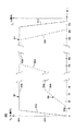
電界放射ディスプレイの概要を提示する。図1は、FEDフラット・パネル・ディスプレイの一部の横断面図であり、多層構造75を示す。多層構造75は、基板構造とも呼ばれる電界放出バックプレート構造45と、電子受信フェースプレート構造70とを含む。画像は、フェースプレート構造70に生成される。バックプレート構造45は、一般的に、電気的絶縁バックプレート65、エミッタ(又は、カソード)電極60、電気的絶縁層55、パターニングされたゲート電極50、及び、絶縁層55を貫く開口部に置かれた円錐形の電子放出素子40、から成る。電子放出素子40の1つのタイプは、Twichellらに1997年3月4日に発行された米国特許第5,608,283号に記載されており、別のタイプは、Spindtetらに1997年3月4日に発行された米国特許第5,607,335号に記載されている。これらは、いずれもここに参考文献として組み込まれる。電子放出素子40の先端は、ゲート電極50の対応する開口部を通って露出している。エミッタ電極60及び電子放出素子40は、一緒に、FEDフラット・パネル・ディスプレイの図示した部分75のカソードを構成している。フェースプレート構造70は、電気的絶縁フェースプレート15、アノード20、及び、蛍光体コーティング25によって構成される。素子40から放出された電子は、蛍光体部分30によって受信される。一実施形態において、電子放出素子40は、円錐形のモリブデン先端を含む。本発明の他の実施形態において、アノード20は蛍光体25上に配置され、エミッタ40はフィラメントなどの他の幾何学的形状を含む。
【0021】
電子放出素子40からの電子の放出は、適切な電圧(VG)をゲート電極50に印加することによって制御される。別の電圧(VE)は、エミッタ電極60によって直接電子放出素子40に印加される。ゲート−エミッタ電圧(例えば、VG−VE又はVGE)が増えると、電子放出が増える。高電圧(VC)をアノード20に印加することによって、電子が蛍光体25へ向けられる。適切なゲート−エミッタ電圧VGEが印加されると、電子は、様々な値のオフノーマル放出角度θ42で電子放出素子40から放出される。放出された電子は、図1のライン35によって示された非線形な(例えば、放物線状の)軌道をたどり、蛍光体25のターゲット部分と衝突する。このように、VG及びVEは、放出電流(IC)の大きさを決定し、アノード電圧Vcは、所定の角度で放出された所定の電子に対して、電子軌道の方向を制御する。
【0022】
図2は、例示的FEDスクリーン100の一部を示す。FEDスクリーン100は、水平に並べられた行(row)及び垂直に並べられた列(column)から成るピクセルの配列(array)に再分割される。各ピクセル125の境界は、破線で示される。3本の別々の行ライン230が図示されている。各行ライン230は、この配列のピクセル行のうちの1つのための行電極である。一実施形態において、各行ライン230は、電極と関連付けられた特定の行の各エミッタのエミッタ・カソードに接続される。図2に示した一ピクセル行の一部は、一対の隣接したスペーサ壁135の間に配置される。他の実施形態において、スペーサ壁135は、各行の間にある必要はない。そして、ディスプレイの中には、スペース壁135は存在しないものもある。ピクセル行は、1つの行ライン230に沿ったすべてのピクセルを含む。2以上のピクセル行(及び、24〜100ほどのピクセル行)は、一般的に、隣接したスペーサ壁135の各ペアの間に配置される。
【0023】
カラー・ディスプレイでは、ピクセルの各列は、3本の列ライン250:(1)赤用のライン;(2)緑用のライン;及び(3)青用のライン、を有する。同様に、各ピクセル列は、各蛍光体ストリップ(赤、緑、青)の1つを含み、トータルで3つのストリップを含む。モノクロ・ディスプレイにおいて、各列は、ストリップを1つだけ含む。本実施形態において、列ライン250の各々は、関連する列の各エミッタ構造のゲート電極に接続される。さらに、本実施形態において、列ライン250は、列駆動回路(図示せず)に接続され、行ライン230は、行駆動回路(図示せず)に接続される。
【0024】
作動中、赤、緑、及び、青の蛍光体ストリップは、エミッタ・カソード60/40の電圧に対して高い正の電圧に維持される。電子放出素子群の1つが対応する行ライン230及び列ライン250の電圧を調整することによって適切に励起されると、その素子群の素子40は、対応した色の蛍光体のターゲット部分30に向けて加速された電子を放出する。すると、励起した蛍光体が光を発する。スクリーン・フレーム・リフレッシュ・サイクル(例えば、約60Hzのレートで実行される)の間、行は一度に1つだけアクティブとなり、列ラインは、その一ピクセル行を定期的に照射するように、電圧が印加される。これは、すべてのピクセル行が照射されてフレームを表示するまで、一行ずつ、時間的に連続して実行される。上記のFED構成は、以下の米国特許により詳細に記載されている;Duboc,Jr.らに1996年7月30日に発行された米国特許第5,541,473号;Spindtらに1996年9月24日に発行された米国特許第5,559,389号;Spindtらに1996年10月15日に発行された米国特許第5,564,959号;及び、Havenらに1996年11月26日に発行された米国特許第5,578,899号。これらは、ここに参考文献として組み込まれる。
【0025】
(本発明の一実施形態に係るFED調整手順)
本発明は、新しく組み立てられたFEDを調整してその中に含まれている汚染物質の種を取り除くプロセスを提供する。この調整プロセスは、FED装置がノーマルなオペレーションに用いられる前に実行されるものであり、通常、製造中に実行される。本発明の調整プロセスの間、FEDの真空管の中に含まれる汚染物質に大量の電子が衝突する。この衝突の結果として、汚染物質は打ち落とされ、ガス・トラッピング装置(例えば、ゲッター)によって収集される。新しく組み立てられたFEDは大量の汚染物質を含んでいるため、本発明に係る調整プロセスにおいてアーク放電が発生しないように用心深い工程が取られなければならない。このため、本発明によれば、調整プロセスは、アノードに所定の高電圧を印加する工程と、その後、放出カソードにより電子がアノードへ引っ張られるようにする工程と、を含む。本発明の一実施形態の増進のために、放出電流は、アノード電圧が所定の高電圧に達した後に、最大値までゆっくりと増加させる。
【0026】
図3は、本実施形態の調整プロセスにおける特定のFEDのアノード電圧レベル及び放出電流レベルの変化を示すプロット300を示す。プロット301は、アノード電圧(VC)の変化を示し、プロット302は、放出電流(IC)の変化を示す。特に、VCは、ドライバ・エレクトロニクスによって供給される最大アノード電圧に対するパーセントとして表している。例えば、高電圧蛍光体に対して、最大アノード電圧は、例えば、3,000ボルトである。この最大アノード電圧は、アノードの正常な作動電圧ではないことに注意。例えば、ディスプレイ・スクリーンの正常な作動電圧は、最大アノード電圧の25%〜75%である。ICは、FEDの駆動回路によって供給される最大放出電流に対するパーセントとして表している。FEDに対して高電圧及び大電流を供給するドライバ・エレクトロニクス及び電子機器は、本分野ではよく知られているため、本発明の態様が分かりにくくなるのを避けるために、ここでは説明しない。
【0027】
本発明によれば、プロット301は、電圧増加区間301a、第一の水平区間301b、及び、電圧減少区間301cを含み、プロット302は、第一の電流増加区間302a、第二の電流増加区間302b、第二の水平区間302c、第三の電流増加区間302d、第三の水平区間302e、及び、電流減少区間302fを含む。図示した特定の実施形態では、電圧増加区間301aにおいて、VCは、約5分掛けて、最大アノード電圧の0%から100%までに増加する。注目に値すべきなのは、電子がゲート電極ではなくディスプレイ・スクリーン(アノード)へ引き寄せられるように、VCの増加中、ICが0%のままであることである。
【0028】
VCが最大アノード電圧の100%に達した後、VCは、約25分間、その電圧レベルに維持される。同時に、ICは、約10分掛けて、最大放出電流の0%から1%までゆっくり増加する(第一の電流増加区間302a)。その後、ICは、約20分掛けて、最大放出電流の50%までゆっくり増加する(第二の電流増加区間302b)。ICは、次いで、約10分間、その50%レベルに維持される(第三の水平区間302c)。本発明によれば、ICは、電子エミッタの脱離によって形成される高イオン圧ゾーンの形成を回避するために、ゆっくりとした速度で増加される。脱離した分子は、アーク放電のリスクを増加させ得る高イオン圧の小さいゾーンを形成し得る。このように、放出電流をゆっくり増加させることによって、アーク放電の発生が大幅に低減される。
【0029】
図3によれば、次いで、ICは、「ソーキング(soaking)」が発生しているため、約10分間、一定のレベルに維持される(第三の水平区間302c)。ソーキングは、ガス・トラッピング装置によって汚染物質種が取り除かれるプロセスを指す。一般的には「ゲッター(getter)」として知られているガス・トラッピング装置は、この調整プロセス段階で、本発明によって用いられ、本分野ではよく知られている。
【0030】
一実施形態において、ソーキング期間後、ICは、次いで、その最大レベルである100%まで増加され(第三の電流増加302d)、その後、約2時間、そのレベルに維持される(第四の水平区間302e)。同時に、VCは、その最大レベルに維持される。その後、VC及びICは、これらの各最大値の0%まで戻る。注目に値すべきなのは、図3の区間302f及び301cに示すように、VCがターンオフされる前に、ICがターンオフされることである。このようにして、すべての放出された電子がディスプレイ・スクリーン(アノード)に引き寄せられ、ゲート−エミッタ電流が防止される。
【0031】
本発明の調整プロセスにおいて、あらゆる打ち落とされた又は他の方法でリリースされた汚染物質は、ガス・トラッピング装置(「ゲッター」としても知られる)によって収集される。ゲッターは、上述のように、本分野では良く知られている。図3に示した特定の実施形態において、調整期間全体は、約6時間である。この調節期間後に、汚染物質のほとんどは、打ち落とされ、ゲッターによって収集されており、新たに組み立てられたFEDスクリーンは、ノーマル・オペレーションの準備が整う。
【0032】
例えばCH(4)などの一部のガス種は、ゲッターによって汲み上げられない。これらの種は、チューブ・オペレーションによって汲み上げられる。電子は、ばらばらに壊れて、ガス分子をイオン化する。イオンは、電界によってカソード及びフェースプレートへ加速される。
【0033】
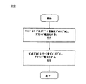
図4は、本発明に係るFED調整プロセスの工程を示すフローチャート400である。本発明の説明を容易にするために、フローチャート400は、図1に示した例示的なFED構造75と共に説明される。ここで図1及び4を参照すると、ステップ410において、FEDのアノード20は、高電圧に駆動される。ステップ410において、放出電流(IC)は最大レベルの0%に維持されており、よってオフである、ことに注意。本発明の一実施形態において、ゲート電極50及びエミッタ−カソード60/40の電圧は、グラウンドに維持される。電子が、一旦放出されると、ゲート電極50ではなくアノード20へ引き寄せられるように、放出電流を0%に維持しながら、アノード電圧は高電圧に駆動される。
【0034】
図4のステップ420において、放出電流ICは、FEDのドライバ・エレクトロニクスによって供給される最大放出電流の1%までゆっくり増加される。本発明の特定の一実施形態において、ステップ420は、完了するまで約5分掛かる。このゆっくりとした増加により、電子エミッタの脱離によって高イオン圧の局所的ゾーンが形成されない。さらに、本実施形態において、ファウラー・ノルドハイム理論によって予測されるように、放出電流ICは、ゲート−エミッタ電圧(VGE)に比例する。このように、本実施形態において、放出電流ICは、ゲート−エミッタ電圧VGEを調整することによって制御できる。
【0035】
図4のステップ430において、放出電流ICは、FEDのドライバ・エレクトロニクスによって供給される最大放出電流の約50%まで増加される。一実施形態において、ステップ430は、完了するまで約10分掛かる。ステップ420と同じように、このゆっくりとした増加により、脱離した分子には拡散するのに十分な時間を与えられるため、高イオン圧の局所的ゾーンは形成されない。
【0036】
図4のステップ440において、放出電流IC及びアノード電圧VCは、大量の電子が放出されるように、それらの各最大値の100%に維持される。放出された電子は、前の組立プロセスによって取り除かれたほとんどの緩んだ汚染物質に衝突して打ち落とす。打ち落とされた汚染物質は、次いで、ゲッターなどのイオン・トラッピング装置によって捕獲される。上述のように、ゲッターは、本分野では良く知られているため、本発明の態様が分かりにくくなるのを避けるために、ここでは説明しない。
【0037】
ステップ450において、放出電流は、最大値の0%に戻される。その後、ステップ460において、アノード電圧は、その最大値の0%まで戻される。重要なことは、すべての放出された電子がアノードに引き寄せられるように、アノード電圧をターンオフする前に、放出電流をターンオフすることである。
【0038】
図5は、本発明の一実施形態に係る調整プロセスを制御する装置を示すブロック図700である。図1のFED75の略図も示す。図5を参照すると、本装置は、FED75と接続するように構成されたコントローラ回路710を含む。特に、コントローラ回路710は、FED75のアノード20にアノード電圧を供給する第一の電圧制御回路710aを含む。コントローラ回路710は、更に、ゲート電極50にゲート電圧を供給する第二の電圧制御回路710bと、エミッタ・カソード60/40にエミッタ電圧を供給する第三の電圧制御回路710cと、を含む。明らかなように、コントローラ回路710は一例であり、コントローラ回路710の多くの異なる実施例も使用され得る。
【0039】
作動中、電圧制御回路710a〜cは、様々な電圧をFED75のアノード20、ゲート電極50、及び、エミッタ電極60/40に供給し、本発明の調整プロセス中に異なる電圧及び放出電流を提供する。本発明の一実施形態において、コントローラ回路710は、非常に高電圧を提供するために本調整プロセスのために特別に作られたスタンドアロンの電子機器である。しかし、明らかなように、コントローラ回路710は、FEDに内蔵され、FEDのターンオン/ターンオフ中にアノード電圧及び放出電流を制御してもよい。
【0040】
(本発明のFEDターンオン/ターンオフ手順)
本発明は、FEDユニットの電源オン/オフ中のアーク放電のリスクを最小限に抑える電界放射ディスプレイの操作方法も提供する。特に、本発明の一実施形態によれば、本FED操作方法は、FEDのアノード・ディスプレイ・スクリーンに電源を入れる工程と、その後、放出カソードに電源を入れる工程と、を含む。本発明の別の実施形態によれば、アーク放電のリスクを最小限に抑えたFED操作方法は、放出カソードの電源を切る工程と、その後、アノード・ディスプレイ・スクリーンの電源を切る工程と、を含む。本発明によれば、以上の工程に従うことによって、アーク放電の発生は大幅に低減される。
【0041】
図6は、本発明の別の実施形態に係るFEDターンオン手順の工程のフローチャート500を示す。本発明の説明を容易にするために、フローチャート500は、図1の例示的FED75と共に説明される。ここで図1及び6を参照すると、ステップ510において、FED75がスイッチオンされると、アノード20がイネーブルされる。本実施形態において、アノードは、所定の閾値電圧(例えば、300V)の印加によって、イネーブルされる。さらに、本発明において、アノードは、アノード20に電力を供給する電源回路(図示せず)をスイッチオンすることによって、イネーブルされてもよい。FED用の電源装置は、本分野では良く知られており、良く知られた電源装置をいくつでも本発明と共に用いることができる。
【0042】
ステップ520において、FED75のアノード20がイネーブルされ、アノードが所定の閾値電圧に達すると、次いで、FED75のエミッタ・カソード60/40及びゲート電極50がイネーブルされる。本発明において、電子をアノード20へ向け、電子がゲート電極50に衝突することを回避するためにアノード20がイネーブルされてから所定期間後、FED75のエミッタ・カソード60/40がイネーブルされる。一実施形態において、エミッタ・カソード60/40及びゲート電極50は、FEDの行及び列駆動回路(図示せず)をスイッチオンすることによってもイネーブルできる。
【0043】
図7は、本発明の別の実施形態に係るFEDターンオフ手順の工程を示すフローチャート600である。以下、フローチャート600は、図1の例示的FED75と共に説明される。ここで図1及び7を参照すると、ステップ610において、FEDがスイッチオフされると、FED75のエミッタ・カソード60/40及びゲート電極50がディスエブルされる。同時に、アノード20は、高電圧のままである。さらに、一実施形態において、エミッタ・カソード60/40及びゲート電極50は、行ドライバ及びと列ドライバ(図示せず)によって供給される行電圧及び列電圧をそれぞれグラウンド電位に設定することによって、ディスエブルされる。
【0044】
ステップ620において、エミッタ・カソード60/40及びゲート電極50がディスエブルされた後、FEDのアノード20がディスエブルされる。本発明によれば、ステップ620が、放出カソードから放出されたすべての電子がアノード・ディスプレイ・スクリーンに引き寄せられるように、ステップ610の後で実行される。一実施形態において、アノード20は、アノード20に電力を供給する電源回路(図示せず)をスイッチオフすることによってディスエブルされる。このようにして、FEDにおけるアーク放電の発生が最小限に抑えられる。
【0045】
(本発明の別の実施形態に係るFED調整プロセス)
図8は、本発明の別の実施形態に係る特定のFED装置を調節する電圧/電流印加手法を示すプロット800である。プロット801は、アノード電圧(VC)の変化を示し、プロット802は、放出電流(IC)の変化を示す。特に、VCは、ドライバ・エレクトロニクスによって供給される最大アノード電圧に対するパーセントで表される。ICは、FEDの駆動回路によって供給される最大放出電流に対するパーセントで表される。
【0046】
本発明によれば、プロット801は、電圧増加区間810a〜d、一定電圧区間820a〜f、電圧減少区間830a〜c、を含み、プロット302は、電流増加区間840a〜e、一定電流区間850a〜e、及び、電流減少区間860a〜c、を含む。図示した特定の実施形態では、電圧増加区間810aにおいて、VCは、約10分掛けて、最大アノード電圧の0%から50%まで増加される。注目に値すべきなのは、電子がゲート電極ではなくディスプレイ・スクリーン(アノード)へ引き寄せられるように、VCの増加中、ICは0%のままであることである。
【0047】
VCが最大アノード電圧の50%に達すると、VCは、約30分間、その電圧レベルに維持される(一定電圧区間820a)。同時に、ICは、約10分掛けて、最大放出電流の0%から1%までゆっくり増加される(電流増加区間840a)。その後、ICは、約10分掛けて、最大放出電流の50%までゆっくり増加される(電流増加区間840b)。次いで、ICは、約10分間、その50%レベルに維持される(一定電流区間850a)。本発明によれば、ICは、電子エミッタの脱離によって形成される高圧ゾーンの形成を回避するためにゆっくりとした速度で増加される。脱離した分子は、アーク放電のリスクを増加させ得る高圧の小さいゾーンを形成し得る。放出電流をゆっくりと増加させることによって、脱離した分子がガス・トラッピング装置(例えば、ゲッター)に拡散し得る十分な時間が与えられる。このようにして、アーク放電の発生は大幅に低減される。
【0048】
図8によれば、VCは、50%から20%レベルに減少され(電圧減少区間830a)、約30分間、その20%レベルに維持される(一定電圧区間820b)。VCが20%レベルに達すると、ICは100%レベルまでゆっくりと増加される(電流増加区間840c)。この20%レベルは、アノード電圧がFEDのアノードが放出された電子を引き寄せるのに最低限必要な閾値レベルに近くなるように選択されることに注意。次いで、ICは、「ソーキング(soaking)」が発生しているため、約20分間、一定レベルに維持される(一定電流区間820b)。
【0049】
本実施形態において、次いで、ICは、その最大レベルの50%まで減少し(電流減少区間860a)、その後、約20分間、そのレベルに留まる(一定電流区間850c)。ICが50%レベルに達すると、VCは、50%レベルまで増加され(電圧増加区間810b)、20分間、そのレベルに維持される(一定電流レベル820c)。その後、ICは、その最大値の0%へターンオフされる(電流減少区間860b)。
【0050】
ICがターンオフされた後、VCは、約2.5時間掛けて、その最大レベルの100%までゆっくり増加され(電圧増加区間810c)、約1時間の間、その最大レベルに維持される(一定電圧区間820d)。その後、VCは、50%レベルまで減少され(電圧減少区間830b)、約20分間、そのレベルに維持される(一定電圧区間820e)。VCが50%レベルのとき、ICは、0%から50%レベルまでゆっくり増加される(電流増加840d)。次いで、VC及びICは、それらの各最大値の100%まで駆動され(電圧増加区間810d及び電流増加区間840e)、約1.5時間の間、それらのレベルに維持される(一定電圧区間820f及び一定電流区間850e)。その後、VC及びICは、0%まで戻される(電圧減少区間830c及び電流減少区間860c)。
【0051】
注目に値すべきなのは、図8の区間810d及び840eに示すように、VCが最大値に駆動されてからICが最大値へ駆動され、VCがターンオフされる前にICがターンオフされることである。このようにして、すべての放出された電子は、ディスプレイ・スクリーン(アノード)に引き寄せられ、ゲート−エミッタ電流が防止される。
【0052】
(本発明の一実施形態の電源オン/オフ回路の操作使用)
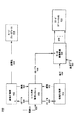
図9は、本発明の一実施形態に係る電源オン/オフ回路910の論理ブロック図を示す。回路910は、FEDスクリーンの正常な作動中に、該スクリーンの電源を入れる/切るのに用いられる。すなわち、回路910は、FEDスクリーンがターンオン及びターンオフされる度に、用いられる。回路910は、FEDスクリーンの電源オン/オフ中のエミッタ電極60(図1)及びゲート電極50(図1)の劣化を低減するための電源オン/オフ手順を実行する。
【0053】
特に、本発明の本実施形態に係る回路910は、エミッタ電極60に電圧が印加される前に、アノード電極20(図1)が高電圧レベルであるようにするために用いられる。この状態において、エミッタ電極60から放出された電子は、アノード電極20に引き寄せられるため、ゲート電極50とのあらゆる接触/衝突が回避される。エミッタからゲート電極への電子放出は、ゲート電極を著しく劣化させる原因となる。また、この電子放出の結果としてゲート電極から除去されたイオンも、エミッタ電極に降り注ぎ、エミッタ電極を同様に劣化させ得る。
【0054】
図9は、回路910の構成要素を示す。シーケンサを含む論理コントローラ916が設けられる。このシーケンサは、内部状態機械によって実現され得る。ライン924からの電源オン信号に応答して、論理コントローラ916は、高電圧電源912に接続されたライン926上に第一のイネーブル信号を生成する。ライン924上の電源オン信号は、オン/オフ・スイッチに対応し得る。確認信号928に応答して、論理コントローラ916は、低電圧電源918に接続されたライン930上に第二のイネーブル信号も生成する。ライン926及び930によってイネーブルされないとき、高/低電圧電源装置は、ディスエブルされる(例えば、それらは電圧レベルを一切出力しない)。高電圧電源は、図9に914として示されたフェースプレートのアノード20(図1)に、電源ライン934を経由して、接続される。低電圧電源918は、電源ライン938を経由して、行/列駆動回路920にそれらの電圧源として接続される。これら行/列駆動回路は、FED装置内でディスプレイ行列(例えば、ピクセルの行及び列)を構成するゲート電極及びエミッタ電極922に接続される。アナログ駆動電圧が、ゲート及びエミッタ電極(合わせて「カソード」と呼ぶ)に接続されたライン940上に印加される。
【0055】
高電圧電源912は、ライン926によってイネーブル/ディスエブルし得る出力934を有する。高電圧電源912は、該電源から出力された高電圧の存在又は不存在を示す論理レベル信号を提供する。これは、ライン928上に生成される確認信号と呼ばれ、この確認信号は、高電圧電源912の作動電圧がその出力上で実現されたときに、生成される。この確認信号ライン928は、制御ロジック916に接続される。一実施形態において、高電圧電源912の電圧レベルは、例えば、5,000〜10,000ボルトである。イネーブル信号926が取り除かれると、高電圧電源912はスタンバイ状態(例えば、ライン934上の出力がゼロで、入力電流が最小のモード)に入る。
【0056】
低電圧電源918は、ライン930によってイネーブル/ディスエブルし得る出力938を有する。低電圧電源918は、任意で、該電源から出力された低電圧の存在又は不存在を示す論理レベル信号を提供してもよい。この任意の確認信号は、ライン932上に生成され、低電圧電源918の作動電圧がその出力上で実現されたときに、生成される。この任意の確認信号ライン932は、制御ロジック916に接続される。一実施形態において、低電圧電源918の電圧レベルは、エミッタ及びゲートに必要な電位を供給するのに十分なものであり、例えば−20〜+15ボルトである。イネーブル信号930が取り除かれると、低電圧電源918はスタンバイ状態(例えば、ライン938上の出力がゼロで、入力電流が最小のモード)に入る。
【0057】
また、図9の制御ロジック916も、行/列駆動回路920をイネーブルする第三のイネーブル信号をライン936上に生成する。駆動回路920は、(ライン942からの)ビデオ画像情報を各エミッタ・グループに特有の電気的電位940に変換する。駆動回路920の出力は、ライン936を経由して、イネーブル/ディスエブルし得る。イネーブル信号936が取り除かれると、駆動回路920はスタンバイ状態(例えば、ライン938上の出力がゼロで、入力電流が最小のモード)に入る。駆動回路920は、低電圧電源918から電圧供給を受けるように接続される。
【0058】
図9に示すように、ゲート及びエミッタ電極をイネーブルするためには、イネーブル信号930及び936の双方が必要とされる。アノード電極をイネーブルするためには、イネーブル信号926が必要とされる。
【0059】
図10は、本発明の一実施形態に係る図9の回路の制御ロジック回路によって実行される制御工程を概説した状態図を示す。このシーケンスは、アノード電位が存在しない限り、FEDが電子を放出しないことを保証している。これにより、エミッタ及びゲートの劣化をもたらし得るアノード電位無しで電子が放出されるという状態が阻止される。
【0060】
より具体的には、図10は、制御ロジック916の例示的な状態機械実施例の状態を示す。初期状態950において、パワはオフで、図9のすべての電源及び駆動回路はディスエブルされている。電源オン信号に応答して、状態952に入る。状態952では、イネーブル・ライン926が起動され、よって高電圧電源912がイネーブルされる。高電圧電源912がその出力においてその作動電圧を確立すると、確認信号が制御ロジック916に供給され、よって状態954に入る。状態954では、制御ロジック916は、ライン930上にイネーブル信号を生成し、ディスエブルされている低電圧電源918をイネーブルする。
【0061】
所定時間(遅延期間)の経過に応答して、或いは、任意のライン932上の確認信号に応答して、状態956に入る。状態956において、制御ロジック916は、ライン936上にイネーブル信号を生成し、駆動回路920をイネーブルする。状態956において、FEDスクリーンは、完全に電力が供給され、使用可能な状態となっている。そこで、ビデオ情報をFEDスクリーン上に提示することができる。明らかなように、アノードだけが完全に電源オンされた後でゲート及びエミッタ電極の電源をオンすることによって、本発明は、エミッタ及びゲート電極の劣化を大幅に低減する回路910を提供する。換言すれば、エミッタからゲート電極への電子放出は、回路910によって大幅に低減される及び/又は取り除かれる。
【0062】
また、図10は、制御ロジック916の電源オフ状態も示す。状態956から、ライン924上の電源オフ信号に応答して(例えば、オン/オフ・スイッチに応答して)、状態958に入る。状態958において、駆動回路920がライン936を通じてディスエブルされ、また低電圧電源918がライン930を通じてディスエブルされる。所定時間(遅延時間)の経過に応答して、或いは、任意のライン932上の確認信号に応答して、状態960に入る。状態960において、高電圧電源912はライン926を通じてディスエブルされる。その際、状態950に入る。
【0063】
(フェースプレート電圧を検出する代替方法)
以下、上記方法及びシステムに加えて、フェースプレート上の電圧の存在を検出する代替方法を説明する。高電圧の検出は、行/列バイアス電圧の連動を制御する。これにより、フェースプレート高電圧が存在せず、電子がカソード及び壁と衝突して、ガス抜け及び不均一な放出が生じ得るときに、カソードからの電子の放出が防止される。以下、高電圧電源によって生成された信号を用いることに加えて、フェースプレート上の高電圧を検出する方法について説明する。
【0064】
一実施形態において、高電圧源の印加は、フォーカス・ワッフル(focus waffle)への電流を監視・検出することによって、検出できる。フォーカス・ワッフルは、本発明の譲受人に譲り受けられ、1996年6月18日に発行された米国特許第5,528,103号により詳細に記載されている。この特許文献は、参考文献としてここに組み込まれる。本実施形態において、本システムは、フォーカス・ワッフルからの電流が安定するまで、一時停止される。最終的な電流値は、壁TCRによる周辺温度に依存する。電流が安定すると、行及び列がイネーブルされ、カソードがイネーブルされる。
【0065】
別の実施形態において、フェースプレートでの電圧上昇は、フェースプレート上のフォーカス・ワッフル又は導体層(帯電防止カバーなど)のいずれかを通じて容量性的に検出される。静電容量がより高いため、フェースプレート上の層からの信号の方がフォーカス・ワッフルからの信号よりも大きくなることは明らかである。電圧が安定するか又は高電圧ポイントに到達したとき、行及び列がイネーブルされ、カソードがイネーブルされる。
【0066】
別の実施形態において、フェースプレートへの静電気力は、フェースプレートの邪魔にならない隅に置かれたマイクロメカニカル(MEMS)力検出器を用いて、検出される。この力が高電圧レベルに対応した所定のレベルに達すると、行及び列がイネーブルされ、カソードがイネーブルされる。
【0067】
別の実施形態において、電力がオン(例えば、高電圧)のときはいつでも(好ましくはパルス・モードで)起動しているトリガ又は「スイート」・スポット(ピクセル)が、カソードの隅に配置される。そして、光出力は、トリガ・スポット上で小さい蛍光体パッチから検出される。このトリガ・スポットからの電子は、フェースプレート高電圧は存在しないとき、一部のカソードにガス抜けを起こさせるが、カソード全体を動かすよりはずっと少ない。トリガ・スポットが照射すると、行及び列がイネーブルされ、カソードがイネーブルされる。この同じ手法を用いて、追加的スイート・スポットをパルシングすることによって生じた交流信号をフェースプレートにおいて検出することもできる。この電流信号は、電子がフェースプレートに当たっており、何らかの高電圧が存在しているにちがいない、ことを示す。次いで、この電流信号は、行及び列がイネーブルされること、及び、カソードがイネーブルされること、をトリガする。本実施形態に関して、アノード・セクションへの電流を別途測定できるように、アノードの残りと電源とを抵抗を通じて接続するアノード・セクションへの別個の接続を用いることもできる。
【0068】
大まかにまとめると、この文書は、エミッタ電極及びゲート電極の劣化から保護する電界放射ディスプレイ(FED)の素子をターンオン/ターンオフする回路及び方法について開示している。本回路は、一実施形態において状態機械を用いて実現可能なシーケンサを備えた制御ロジックを含む。電源がオンされると、この制御ロジックは、アノード電極に電圧を供給する高電圧電源にイネーブル信号を送る。この時点で、低電圧電源及び駆動回路はディスエブルされている。高電圧電源から確認信号を受信すると、制御ロジックは、駆動回路に電圧を供給する低電圧電源をイネーブルする。低電圧電源から確認信号を受信すると、或いは、任意で、所定時間が経過すると、制御ロジックは、FED装置の行及び列を構成するゲート電極及びエミッタ電極を駆動する駆動回路をイネーブルする。パワダウンすると、制御ロジックは、まず、低電圧電源をディスエブルし、次に、高電圧電源をディスエブルする。以上は、FEDのノーマルなオペレーション使用中に、FEDが電源オン/オフされる度に、行われる。こうすることによって、本発明の実施形態は、エミッタ電極からゲート電極への直接的な電子放出を制限することによって、エミッタ電極及びゲート電極の劣化を低減する。
【0069】
このように、本発明、エミッタ及びゲート電極の劣化を低減するためにノーマル・オペレーション中にFEDの電源をオン/オフする方法及び回路、について開示した。明らかなように、本発明を実現する電子回路、特に閾値電圧電位が確立されるまで放出カソードの起動を遅らせる回路、は良く知られている。例えば、本開示を読めば当業者には明らかなように、電子制御信号に反応する制御回路を用いて、アノード電圧を感知し、アノード電圧が閾値に達した後で行及び列ドライバへの電源をターンオンする、こともできる。また、明らかなように、本発明を特定の実施形態において説明してきたが、本発明はそれら実施形態によって限定されると解釈されるべきではなく、下記請求項に従って解釈されるべきである。
【図面の簡単な説明】
【0070】
【図1】行ラインと列ラインの交差に配置されたゲート電界放出器を用いる例示的フラット・パネルFEDスクリーンの一部の断面構造図である。
【図2】本発明の一実施形態に係る例示的FEDスクリーンを示す図である。
【図3】本発明の一実施形態に係るFED装置をターンオンするための電圧及び電流印加手法を示す図である。
【図4】本発明の一実施形態に係るFED調整プロセスの工程のフローチャートである。
【図5】本発明の一実施形態に係るFED調整システムのブロック図である。
【図6】本発明の別の実施形態に係るFEDターンオン手順の工程のフローチャートである。
【図7】本発明の別の実施形態に係るFEDターンオフ手順の工程のフローチャートである。
【図8】本発明の別の実施形態に係るFED装置をターンオンするための電圧及び電流印加手法を示す図である。
【図9】FEDスクリーンのノーマル・オペレーション中の該スクリーンの電源オン/オフに用いられる、本発明の一実施形態に係る回路の論理ブロック図である。
【図10】本発明の一実施形態に係る図9の回路の制御ロジック回路によって実行される制御工程を概説した状態図である。【Technical field】
[0001]
The present invention relates to the field of flat panel display screens, and more particularly, to the field of flat panel field emission display screens.
[Background Art]
[0002]
Flat panel field emission displays (FEDs), like standard cathode ray tube (CRT) displays, generate light by impinging high-energy electrons on phosphor screen pixels. The excited phosphor then converts the electron energy to visible light. However, unlike conventional CRT displays that use one (and possibly three) electron beams to scan the phosphor screen in a raster pattern, FEDs use a stationary electron beam for each color element of each pixel. This requires only a very short electron source-to-screen distance as compared to the electron source-to-screen distance required for a conventional CRT scanning electron beam. In addition, FEDs consume significantly less power than CRTs. These factors make FEDs ideal for portable electronic products such as laptop computers, pagers, mobile phones, pocket televisions, PDAs, and handheld game consoles.
[0003]
One of the problems with FEDs is that the FED tubes contain trace amounts of contaminants that can adhere to the surface of the electron-emitting devices, faceplates, gate electrodes, focus electrodes (such as dielectric and metal layers), and spacer walls. That may be. These contaminants can be swept away when electrons of sufficient energy collide. Thus, when the FED is turned on or off, it is likely that these contaminants will form a small high pressure zone within the FED vacuum tube.
[0004]
In addition, electron emission from the emitter electrode to the gate electrode can cause deterioration of both the emitter and the gate. For example, if the gate is positive with respect to the emitter, electrons are drawn from the emitter electrode to the gate electrode. In addition, the presence of high pressure promotes electron emission from the emitter to the gate electrode. This can cause some electrons to collide with the gate electrode instead of the display screen. This situation can lead to gate electrode degradation, such as overheating of the gate electrode. Also, emission to the gate electrode can affect the voltage difference between the emitter and the gate electrode. Also, due to electron emission from the emitter electrode to the gate electrode, ions and other debris may be emitted from the gate and adhere to the emitter electrode. This can cause emitter degradation.
[0005]
It is also worth noting that electrons hit the spacer walls and the focal electrode, causing non-uniform emitter degradation. Problems arise when electrons hit any surface other than the anode. Because these other surfaces are not polished by the electron beam during normal television operation, they are more likely to get dirty and outgas.
[0006]
In addition, when the electrons jump over the gap between the electron-emitting device and the gate electrode, the luminescent emission of the current can also be observed. It can also cause severe damage to sophisticated electron emitters. Of course, this phenomenon, commonly known as "arcing", is highly undesirable.
[0007]
In the past, one way to avoid the arcing problem has been to rub the FED tube manually to remove contaminants. However, it is difficult to remove all contaminants by this method. In addition, the hand rubbing process is time consuming, labor intensive, and unnecessarily increases the cost of manufacturing FED screens.
DISCLOSURE OF THE INVENTION
[Means for Solving the Problems]
[0008]
Accordingly, one embodiment of the present invention provides an improved method of removing contaminant particles from a FED screen. The present invention also provides an improved method and circuit for operating a field emission display that prevents current flow from the gate to the emitter during turn-on and turn-off, thereby reducing the potential for gate and emitter electrode degradation. .
[0009]
These and other advantages of the invention not specifically set forth above will become apparent within the present description of the invention.
[0010]
Embodiments of the present invention provide a method for removing contaminants in a newly assembled field emission display. According to one embodiment of the present invention, the contaminant particles are a) applying a predetermined voltage to the anode of the field emission display (FED), and b) slowly moving the FED after the anode reaches the predetermined voltage. And c) providing an ion trapping device to capture ions and contaminants struck by the emitted electrons. In this embodiment, contaminant species are effectively removed without damaging the FED by applying a predetermined voltage to the anode and slowly increasing the emission current of the FED.
[0011]
Embodiments of the present invention also provide methods and circuits for operating the FED such that current does not flow from the gate to the emitter during turn-on and turn-off. This embodiment protects the emitter and gate from degradation during FED operation. In this embodiment, the method includes the steps of: a) enabling the anode display screen; and b) enabling the electron emitter a predetermined time after the anode display screen has been enabled. In this embodiment, emitted electrons are attracted to the anode by allowing the anode display screen sufficient time to reach a predetermined voltage before the emitter is enabled. In this way, when the FED is turned on, the current from the gate to the emitter, the current from the gate to the spacer, and the current from the gate to the focus are effectively removed. In this embodiment, the anode display screen is enabled by applying a predetermined high voltage to the display screen, and the electron emitter is enabled by bringing the gate and emitter electrodes of the FED to the appropriate voltages. You.
[0012]
In yet another embodiment of the present invention, a method of operating a field emission display to prevent current flow from the gate to the emitter includes the steps of: a) disabling the emitter for a predetermined period of time; Disabling the display screen. In this embodiment, any remaining electrons are attracted to the anode by allowing sufficient time for the electron emitter to be disabled before disabling the anode display screen. In this way, current from the gate to the emitter is removed during the turn-off sequence of the FED. In this embodiment, the anode display screen can be disabled by removing the voltage source from the anode and bringing the anode to ground potential, and the electron emitter can be disabled by bringing the gate and emitter electrodes to ground. Disabled.
[0013]
In yet another embodiment, the present invention includes circuits and methods for turning on and off elements of a field emission display (FED) device to protect the emitter and gate electrodes from degradation. The circuit includes control logic having a sequencer, which in one embodiment may be implemented using a state machine. When powered on, the control logic sends an enable signal to a high voltage power supply that supplies voltage to the anode electrode. At this time, the low-voltage power supply and the driving circuit are disabled. Upon receiving an acknowledgment signal from the high voltage power supply, the control logic enables the low voltage power supply to supply voltage to the drive circuit. Upon receipt of an acknowledgment signal from the low voltage power supply or, optionally, after a predetermined period of time, the control logic enables a drive circuit that drives the gate and emitter electrodes that comprise the rows and columns of the FED device. When powered down, the control logic first disables the low voltage power supply and then disables the high voltage power supply. The above occurs each time the power is turned on / off during normal operation of the FED. By doing so, embodiments of the present invention reduce emitter and gate electrode degradation by limiting direct electron emission from the emitter electrode to the gate electrode, focus electrode, or spacer.
[0014]
In addition to the above, an embodiment of the present invention further includes, in a field emission display, an electron-emitting device for emitting electrons, a gate electrode for controlling electron emission from the electron-emitting device, and a display screen for collecting the electrons. Providing, enabling the display screen to establish a voltage difference between the display screen and the electron-emitting device, and, after enabling the display screen, establishing a voltage difference to direct electrons to the display screen. Enabling the gate electrode by delaying significant electron emission from the electron-emitting device until substantially preventing electrons from hitting the gate electrode.
[0015]
Embodiments of the present invention further include a base plate, a plurality of electron-emitting devices on the base plate, a gate electrode on the base plate for controlling electron emission from the electron-emitting devices, and an electron emitting device spaced from the base plate. A display screen configured to collect electrons emitted from the element and generate an image thereon, and configured to control the flow of electrons to the electron-emitting element, during turn-on of the field emission display device. A control circuit for establishing a voltage difference between the display screen and the electron-emitting device prior to significant electron emission from the electron-emitting device to substantially prevent current from the gate to the emitter. Device.
[0016]
Also, an embodiment is a field emission display device, comprising: a display having a row and a column of pixels, each having an emitter electrode and a gate electrode, each controlled by a drive circuit, and an anode electrode; A high voltage power supply connected to supply a high voltage, connected to receive a first enable signal, and further generating a confirmation signal when its operating voltage is reached; for supplying a low voltage to the drive circuit; A low voltage power supply connected to receive a second enable signal; and a power on connected to a high / low voltage power supply and a driving circuit to prevent electron emission from the emitter to the gate electrode. The first enable signal is generated in response to the signal, and the second enable signal is then generated in response to the acknowledge signal to the display. Comprising a control logic to put a source, a field emission display device having a.
[0017]
Embodiments, in addition to the above, wherein the drive circuit is connected to receive a third enable signal, and the control logic enables the drive circuit by generating a third enable signal after enabling the low voltage power supply. Field emission display device. Embodiments, in addition to the above, also include a field emission display device in which the control logic powers down the display by first disabling the low voltage power supply and then disabling the high voltage power supply. Embodiments, in addition to the above, include a field emission display device wherein the control logic is implemented by a state machine sequencer and further comprising a gas trapping device to capture contaminants in the display.
[0018]
The accompanying drawings, which are incorporated in and constitute a part of this specification, illustrate embodiments of the invention and, together with the description, explain the principles of the invention.
BEST MODE FOR CARRYING OUT THE INVENTION
[0019]
Reference will now be made in detail to this embodiment of the invention. Examples of embodiments are shown in the accompanying drawings and include a method and circuit for powering the FED screen on and off during normal operation to reduce emitter and gate electrode degradation. While the invention will be described in conjunction with the embodiments, it will be apparent that they are not intended to limit the invention to these embodiments. Rather, the invention is intended to cover alternatives, modifications, and equivalents, which may be included within the spirit and scope of the invention as defined by the appended claims. Furthermore, in the following description, for purposes of explanation, numerous specific details are set forth in order to provide a thorough understanding of the present invention. However, it will be apparent to one skilled in the art from reading the present disclosure that the present invention may be practiced without these specific details. In other instances, well-known structures and devices have not been described in detail to avoid obscuring aspects of the present invention.
[0020]
(Overview of field emission display)
An overview of the field emission display is presented. FIG. 1 is a cross-sectional view of a portion of a FED flat panel display, showing a multilayer structure 75. The multilayer structure 75 includes a field emission backplate structure 45, also called a substrate structure, and an electron receiving faceplate structure 70. The image is generated on the faceplate structure 70. The backplate structure 45 is typically located in an electrically insulating backplate 65, an emitter (or cathode) electrode 60, an electrically insulating layer 55, a
[0021]
The emission of the electrons from the electron-emitting
[0022]
FIG. 2 shows a portion of an
[0023]
In a color display, each column of pixels has three column lines 250: (1) a line for red; (2) a line for green; and (3) a line for blue. Similarly, each pixel column includes one of each phosphor strip (red, green, blue), for a total of three strips. In a monochrome display, each row contains only one strip. In this embodiment, each of the column lines 250 is connected to a gate electrode of each emitter structure in the associated column. Further, in the present embodiment, the column lines 250 are connected to a column driving circuit (not shown), and the
[0024]
In operation, the red, green, and blue phosphor strips are maintained at a high positive voltage relative to the voltage at the emitter / cathode 60/40. When one of the electron-emitting devices is properly excited by adjusting the voltage on the
[0025]
(FED adjustment procedure according to one embodiment of the present invention)
The present invention provides a process for conditioning a newly assembled FED to remove contaminant species contained therein. This adjustment process is performed before the FED device is used for normal operation and is typically performed during manufacturing. During the conditioning process of the present invention, large numbers of electrons bombard the contaminants contained within the vacuum tube of the FED. As a result of this collision, contaminants are shot down and collected by a gas trapping device (eg, a getter). Because newly assembled FEDs contain large amounts of contaminants, caution must be taken during the conditioning process according to the present invention to avoid arcing. Thus, according to the present invention, the conditioning process includes applying a predetermined high voltage to the anode, and then causing electrons to be pulled to the anode by the emitting cathode. For enhancement of one embodiment of the present invention, the emission current is slowly increased to a maximum value after the anode voltage reaches a predetermined high voltage.
[0026]
FIG. 3 shows a
[0027]
According to the present invention,
[0028]
V C Reaches 100% of the maximum anode voltage, C Is maintained at that voltage level for about 25 minutes. At the same time, I C Slowly increases from 0% to 1% of the maximum emission current over about 10 minutes (first
[0029]
According to FIG. 3, then I C Is maintained at a constant level for about 10 minutes because "soaking" has occurred (third
[0030]
In one embodiment, after a soaking period, I C Is then increased to its maximum level of 100% (third
[0031]
In the conditioning process of the present invention, any shot down or otherwise released contaminants are collected by a gas trapping device (also known as a "getter"). Getters are well known in the art, as described above. In the particular embodiment shown in FIG. 3, the entire adjustment period is about 6 hours. After this conditioning period, most of the contaminants have been shot down and collected by the getter, and the newly assembled FED screen is ready for normal operation.
[0032]
Some gas species, for example CH (4), are not pumped by the getter. These seeds are pumped by a tube operation. The electrons break apart and ionize gas molecules. The ions are accelerated by the electric field to the cathode and faceplate.
[0033]
FIG. 4 is a
[0034]
In
[0035]
In
[0036]
In
[0037]
In
[0038]
FIG. 5 is a block diagram 700 illustrating an apparatus for controlling an adjustment process according to an embodiment of the present invention. A schematic diagram of the FED 75 of FIG. 1 is also shown. Referring to FIG. 5, the device includes a controller circuit 710 configured to interface with the FED 75. In particular, the controller circuit 710 includes a first voltage control circuit 710a that supplies an anode voltage to the
[0039]
In operation, voltage control circuits 710a-c provide various voltages to
[0040]
(FED turn-on / turn-off procedure of the present invention)
The present invention also provides a method of operating a field emission display that minimizes the risk of arcing during power on / off of the FED unit. In particular, according to one embodiment of the present invention, the present method of operating a FED includes turning on the anode display screen of the FED, and then turning on the emission cathode. According to another embodiment of the present invention, a method of operating an FED that minimizes the risk of arcing comprises turning off the emitting cathode and then turning off the anode display screen. Including. According to the present invention, the occurrence of arc discharge is greatly reduced by following the above steps.
[0041]
FIG. 6 shows a
[0042]
In
[0043]
FIG. 7 is a
[0044]
In
[0045]
(FED adjustment process according to another embodiment of the present invention)
FIG. 8 is a
[0046]
According to the present invention,
[0047]
V C Reaches 50% of the maximum anode voltage, V C Is maintained at that voltage level for about 30 minutes (
[0048]
According to FIG. C Is reduced from the 50% level to the 20% level (
[0049]
In the present embodiment, then, I C Decreases to 50% of its maximum level (current decrease section 860a), and then remains at that level for about 20 minutes (constant
[0050]
I C Is turned off, then V C Is slowly increased to 100% of its maximum level over approximately 2.5 hours (voltage increase interval 810c) and maintained at its maximum level for approximately 1 hour (
[0051]
It should be noted that as shown in
[0052]
(Operation and Use of Power On / Off Circuit of One Embodiment of the Present Invention)
FIG. 9 shows a logical block diagram of the power on / off
[0053]
In particular, the
[0054]
FIG. 9 shows the components of the
[0055]
High
[0056]
Low
[0057]
The
[0058]
As shown in FIG. 9, both enable
[0059]
FIG. 10 is a state diagram outlining the control steps performed by the control logic circuit of the circuit of FIG. 9 according to one embodiment of the present invention. This sequence ensures that the FED does not emit electrons unless the anode potential is present. This prevents a situation in which electrons are emitted without an anode potential that can cause emitter and gate degradation.
[0060]
More specifically, FIG. 10 shows the states of an exemplary state machine embodiment of
[0061]
[0062]
FIG. 10 also shows the power off state of the
[0063]
(Alternative method of detecting faceplate voltage)
In the following, in addition to the above methods and systems, alternative methods for detecting the presence of a voltage on the faceplate will be described. High voltage detection controls the interlocking of the row / column bias voltage. This prevents the emission of electrons from the cathode when there is no faceplate high voltage and electrons can collide with the cathode and the wall, resulting in outgassing and uneven emission. Hereinafter, a method of detecting a high voltage on the face plate in addition to using a signal generated by the high voltage power supply will be described.
[0064]
In one embodiment, the application of a high voltage source can be detected by monitoring and detecting the current to a focus waffle. Focus Waffle is described in more detail in US Pat. No. 5,528,103, issued Jun. 18, 1996, assigned to the assignee of the present invention. This patent document is incorporated herein by reference. In this embodiment, the system is suspended until the current from the focus waffle stabilizes. The final current value depends on the ambient temperature due to the wall TCR. When the current stabilizes, the rows and columns are enabled and the cathode is enabled.
[0065]
In another embodiment, the voltage rise at the faceplate is detected capacitively through either a focus waffle or a conductive layer (such as an antistatic cover) on the faceplate. Obviously, due to the higher capacitance, the signal from the layer on the faceplate will be larger than the signal from the focus waffle. When the voltage stabilizes or reaches the high voltage point, the rows and columns are enabled and the cathode is enabled.
[0066]
In another embodiment, electrostatic forces on the faceplate are detected using a micro-mechanical (MEMS) force detector located in an unobtrusive corner of the faceplate. When this force reaches a predetermined level corresponding to the high voltage level, the rows and columns are enabled and the cathode is enabled.
[0067]
In another embodiment, a trigger or "sweet" spot (pixel) that fires (preferably in pulse mode) whenever power is on (eg, high voltage) is located at the corner of the cathode. . Light output is then detected from the small phosphor patch on the trigger spot. Electrons from this trigger spot, when no faceplate high voltage is present, cause some cathodes to outgas, but much less than moving the entire cathode. When the trigger spot illuminates, the rows and columns are enabled and the cathode is enabled. Using this same approach, the AC signal generated by pulsing the additional sweet spot can also be detected at the faceplate. This current signal indicates that the electrons are hitting the faceplate and some high voltage must be present. This current signal then triggers the row and column to be enabled and the cathode to be enabled. For this embodiment, a separate connection to the anode section may be used that connects the rest of the anode and the power supply through a resistor so that the current to the anode section can be measured separately.
[0068]
Broadly summarized, this document discloses a circuit and method for turning on / off elements of a field emission display (FED) that protects the emitter and gate electrodes from degradation. The circuit includes control logic with a sequencer that can be implemented using a state machine in one embodiment. When the power is turned on, the control logic sends an enable signal to a high voltage power supply that supplies a voltage to the anode electrode. At this point, the low voltage power supply and drive circuit are disabled. Upon receiving an acknowledgment signal from the high voltage power supply, the control logic enables the low voltage power supply to supply voltage to the drive circuit. Upon receipt of an acknowledgment signal from the low voltage power supply or, optionally, after a predetermined period of time, the control logic enables a drive circuit that drives the gate and emitter electrodes that comprise the rows and columns of the FED device. When powered down, the control logic first disables the low voltage power supply, and then disables the high voltage power supply. The above is performed each time the power of the FED is turned on / off during the normal operation of the FED. By doing so, embodiments of the present invention reduce degradation of the emitter and gate electrodes by limiting direct electron emission from the emitter electrode to the gate electrode.
[0069]
Thus, the present invention has disclosed a method and circuit for turning on / off the power of a FED during normal operation to reduce degradation of the emitter and gate electrodes. As will be apparent, electronic circuits embodying the present invention, particularly those that delay the activation of the emission cathode until a threshold voltage potential is established, are well known. For example, it will be apparent to one skilled in the art, after reading this disclosure, that a control circuit responsive to an electronic control signal is used to sense the anode voltage and supply power to the row and column drivers after the anode voltage reaches a threshold. Can be turned on. Also, as will be apparent, while the invention has been described in particular embodiments, the invention should not be construed as limited by those embodiments, but rather according to the following claims.
[Brief description of the drawings]
[0070]
FIG. 1 is a cross-sectional structural view of a portion of an exemplary flat panel FED screen using gated field emitters located at the intersection of row and column lines.
FIG. 2 illustrates an exemplary FED screen according to one embodiment of the present invention.
FIG. 3 is a diagram illustrating a voltage and current application method for turning on the FED device according to an embodiment of the present invention.
FIG. 4 is a flowchart of steps of an FED adjustment process according to an embodiment of the present invention.
FIG. 5 is a block diagram of an FED adjustment system according to an embodiment of the present invention.
FIG. 6 is a flowchart of the steps of an FED turn-on procedure according to another embodiment of the present invention.
FIG. 7 is a flowchart of steps of an FED turn-off procedure according to another embodiment of the present invention.
FIG. 8 is a diagram illustrating a voltage and current application method for turning on an FED device according to another embodiment of the present invention.
FIG. 9 is a logic block diagram of a circuit according to one embodiment of the present invention used to power on / off the FED screen during normal operation of the screen.
FIG. 10 is a state diagram outlining the control steps performed by the control logic circuit of the circuit of FIG. 9 according to one embodiment of the present invention.
Claims (30)
各々が駆動回路によって制御される各エミッタ電極及び各ゲート電極を有するピクセルの行及び列と、アノード電極と、を有するディスプレイと、
前記アノード電極に高電圧を供給するために接続された高電圧電源と、
前記駆動回路に低電圧を供給するために接続された低電圧電源と、
前記高/低電圧電源及び前記駆動回路に接続され、前記エミッタから前記ゲート電極への電子放出を防止するために、最初に前記高電圧電源をイネーブルし、次に前記低電圧電源をイネーブルすることによって前記ディスプレイに電源を入れる制御ロジックと、を有することを特徴とする電界放射ディスプレイ装置。A field emission display device,
A display having rows and columns of pixels each having an emitter electrode and each gate electrode each controlled by a drive circuit, and an anode electrode;
A high voltage power supply connected to supply a high voltage to the anode electrode;
A low-voltage power supply connected to supply a low voltage to the drive circuit;
First enabling the high voltage power supply and then enabling the low voltage power supply to prevent electron emission from the emitter to the gate electrode connected to the high / low voltage power supply and the drive circuit; Control logic for turning on the display by means of a display device.
前記制御ロジックは、前記低電圧電源をイネーブルした後に前記駆動回路をイネーブルする、ことを特徴とする電界放射ディスプレイ装置。The field emission display device according to claim 1,
The field emission display device according to claim 1, wherein the control logic enables the driving circuit after enabling the low voltage power supply.
前記高電圧電源は、その作動電圧に達すると確認信号を生成し、
前記制御ロジックは、前記高電圧電源へのイネーブル信号を生成することによって前記高電圧電源をイネーブルし、
前記制御ロジックは、前記高電圧電源から前記確認信号を受信したことに応答して前記低電圧電源へのイネーブル信号を生成することによって、前記低電圧電源をイネーブルする、ことを特徴とする電界放射ディスプレイ装置。The field emission display device according to claim 1,
The high-voltage power supply generates an acknowledgment signal when it reaches its operating voltage;
The control logic enables the high voltage power supply by generating an enable signal to the high voltage power supply;
The control logic enables the low voltage power supply by generating an enable signal to the low voltage power supply in response to receiving the confirmation signal from the high voltage power supply. Display device.
前記エミッタ電極は、円錐形の電子エミッタを有し、
前記円錐形の電子エミッタの各々は、モリブデン先端を有する、ことを特徴とする電界放射ディスプレイ装置。The field emission display device according to claim 1,
The emitter electrode has a conical electron emitter,
A field emission display device, wherein each of said conical electron emitters has a molybdenum tip.
前記ディスプレイ内の汚染物質を捕獲するガス・トラッピング装置を更に有する、ことを特徴とする電界放射ディスプレイ装置。The field emission display device according to claim 1,
A field emission display device, further comprising a gas trapping device for trapping contaminants in the display.
各々が駆動回路によって制御される各エミッタ電極及び各ゲート電極を有するピクセルの行及び列と、アノード電極と、を有するディスプレイと、
前記アノード電極に高電圧を供給するために接続され、第一のイネーブル信号を受信するために接続され、更に、その作動電圧に達すると確認信号を生成する高電圧電源と、
前記駆動回路に低電圧を供給するために接続され、第二のイネーブル信号を受信するために接続された低電圧電源と、
前記高/低電圧電源及び前記駆動回路に接続され、前記エミッタから前記ゲート電極への電子放出を防止するために、最初に前記第一のイネーブル信号を生成し、次に前記確認信号に応答して前記第二のイネーブル信号を生成することによって前記ディスプレイに電源を入れる制御ロジックと、を有することを特徴とする電界放射ディスプレイ装置。A field emission display device,
A display having rows and columns of pixels each having an emitter electrode and each gate electrode each controlled by a drive circuit, and an anode electrode;
A high voltage power supply connected to supply a high voltage to the anode electrode, connected to receive a first enable signal, and further generating a confirmation signal when the operating voltage is reached;
A low voltage power supply connected to supply a low voltage to the drive circuit and connected to receive a second enable signal;
Connected to the high / low voltage power supply and the drive circuit to generate the first enable signal first and to respond to the confirmation signal to prevent electron emission from the emitter to the gate electrode; Control logic for turning on the display by generating the second enable signal.
前記駆動回路は、第三のイネーブル信号を受信するために接続され、
前記制御ロジックは、前記低電圧電源をイネーブルした後、前記第三のイネーブル信号を生成することによって前記駆動回路をイネーブルする、ことを特徴とする電界放射ディスプレイ装置。The field emission display device according to claim 6, wherein
The drive circuit is connected to receive a third enable signal;
The field emission display device according to claim 1, wherein the control logic enables the driving circuit by generating the third enable signal after enabling the low voltage power supply.
前記第三のイネーブル信号は、前記低電圧電源がイネーブルされてから所定時間後に生成される、ことを特徴とする電界放射ディスプレイ装置。The field emission display device according to claim 7, wherein
The field emission display device according to claim 1, wherein the third enable signal is generated a predetermined time after the low-voltage power supply is enabled.
前記低電圧電源は、その作動電圧に達すると確認信号を生成し、
前記第三のイネーブル信号は、前記制御ロジックが前記低電圧電源から前記確認信号を受信した後に生成される、ことを特徴とする電界放射ディスプレイ装置。The field emission display device according to claim 7, wherein
The low voltage power supply generates an acknowledgment signal upon reaching its operating voltage;
The field emission display device according to claim 1, wherein the third enable signal is generated after the control logic receives the confirmation signal from the low voltage power supply.
前記制御ロジックが状態機械シーケンサによって実現される、ことを特徴とする電界放射ディスプレイ装置。The field emission display device according to claim 1 or 7,
A field emission display device wherein the control logic is implemented by a state machine sequencer.
前記制御ロジックは、最初に前記低電圧電源をディスエブルして、次に前記高電圧電源をディスエブルすることによって、前記ディスプレイをパワダウンする、ことを特徴とする電界放射ディスプレイ装置。The field emission display device according to claim 1 or 7,
A field emission display device, wherein the control logic powers down the display by first disabling the low voltage power supply and then disabling the high voltage power supply.
前記高電圧は、5,000〜10,000ボルトの範囲内である、ことを特徴とする電界放射ディスプレイ装置。The field emission display device according to claim 1 or 7,
The field emission display device, wherein the high voltage is in the range of 5,000 to 10,000 volts.
前記エミッタ電極は、円錐形の電子エミッタを有する、ことを特徴とする電界放射ディスプレイ装置。The field emission display device according to claim 1 or 7,
The field emission display device, wherein the emitter electrode has a conical electron emitter.
前記円錐形の電子エミッタのそれぞれは、モリブデン先端を有する、ことを特徴とする電界放射ディスプレイ装置。The field emission display device according to claim 13,
A field emission display device, wherein each of said conical electron emitters has a molybdenum tip.
前記ディスプレイ内の汚染物質を捕獲するガス・トラッピング装置を更に有する、ことを特徴とする電界放射ディスプレイ装置。The field emission display device according to claim 7, wherein
A field emission display device, further comprising a gas trapping device for trapping contaminants in the display.
各々が駆動回路によって制御される各エミッタ電極及び各ゲート電極を有するピクセルの行及び列と、アノード電極と、を有するディスプレイと、
前記アノード電極に高電圧を供給するために接続された高電圧電源と、
前記駆動回路に低電圧を供給するために接続された低電圧電源と、
前記アノード電極において高電圧を検出する検出手段と、
前記高/低電圧電源及び前記駆動回路に接続され、前記検出手段によって前記アノードにおいて高電圧が検出された後で前記低電圧電源をイネーブルすることによって前記ディスプレイに電源を入れる制御ロジックと、を有することを特徴とする電界放射ディスプレイ装置。A field emission display device,
A display having rows and columns of pixels each having an emitter electrode and each gate electrode each controlled by a drive circuit, and an anode electrode;
A high voltage power supply connected to supply a high voltage to the anode electrode;
A low-voltage power supply connected to supply a low voltage to the drive circuit;
Detecting means for detecting a high voltage at the anode electrode;
Control logic connected to the high / low voltage power supply and the drive circuit, the control logic turning on the display by enabling the low voltage power supply after a high voltage is detected at the anode by the detection means. A field emission display device characterized by the above-mentioned.
前記制御ロジックは、電源が入れられると、前記高電圧電源へのイネーブル信号を生成することによって前記高電圧電源をイネーブルし、
前記制御ロジックは、前記検出手段から信号を受信したことに応答して前記低電圧電源へのイネーブル信号を生成することによって、前記低電圧電源をイネーブルする、ことを特徴とするディスプレイ。The display according to claim 16,
The control logic, when powered on, enables the high voltage power supply by generating an enable signal to the high voltage power supply;
The display, wherein the control logic enables the low voltage power supply by generating an enable signal to the low voltage power supply in response to receiving a signal from the detection means.
前記ディスプレイは、フォーカス・ワッフルを更に有し、
前記検出手段は、前記フォーカス・ワッフルへの電流を検出する回路を有する、ことを特徴とするディスプレイ。18. The display of claim 17, wherein:
The display further comprises a focus waffle;
2. The display according to claim 1, wherein said detecting means has a circuit for detecting a current to said focus waffle.
前記ディスプレイは、フォーカス・ワッフルを更に有し、
前記検出手段は、前記フォーカス・ワッフルを通じて前記アノードにおける電圧上昇を容量性的に検出する回路を有する、ことを特徴とするディスプレイ。18. The display of claim 17, wherein:
The display further comprises a focus waffle;
2. The display according to claim 1, wherein said detecting means includes a circuit for capacitively detecting a voltage rise at said anode through said focus waffle.
前記ディスプレイは、前記アノード上に導電層を更に有し、
前記検出手段は、前記導電層を通じて前記アノードにおける電圧上昇を容量性的に検出する回路を有する、ことを特徴とするディスプレイ。18. The display of claim 17, wherein:
The display further comprises a conductive layer on the anode,
The display according to claim 1, wherein said detecting means includes a circuit for capacitively detecting a voltage rise at said anode through said conductive layer.
前記検出手段は、前記アノードへの静電気力を検出しているマイクロメカニカル力検出器を有する、ことを特徴とするディスプレイ。18. The display of claim 17, wherein:
The display according to claim 1, wherein said detecting means includes a micro mechanical force detector for detecting an electrostatic force on said anode.
前記カソードの近くに配置され、電源が入れられたときにパルシングによって起動されるサブピクセルと、
前記サブピクセル上に置かれた蛍光体パッチと、を更に有し、
前記検出手段は、前記サブピクセルから発せられた光を検出する、ことを特徴とするディスプレイ。18. The display of claim 17, wherein:
A sub-pixel located near the cathode and activated by pulsing when powered on;
A phosphor patch disposed on the sub-pixel; and
The display, wherein the detecting means detects light emitted from the sub-pixel.
前記カソードの近くに配置され、電源が入れられたときにパルシングによって起動されるサブピクセルと、
前記サブピクセル上に置かれた独立接続アノード・セクションと、を更に有し、
前記検出手段は、前記サブピクセルに対応する前期アノードからの電流信号を検出する、ことを特徴とするディスプレイ。18. The display of claim 17, wherein:
A sub-pixel located near the cathode and activated by pulsing when powered on;
An independently connected anode section located on the sub-pixel; and
The display, wherein the detecting means detects a current signal from the anode corresponding to the sub-pixel.
前記独立接続アノード・セクションは蛍光体パッチである、ことを特徴とするディスプレイ。24. The display of claim 23,
The display, wherein the independently connected anode section is a phosphor patch.
前記ピクセルの各々が、駆動回路によって制御される各エミッタ電極及び各ゲート電極を有する、電界放射ディスプレイ装置において、該ディスプレイ装置に電源を入れる方法であって、
a)制御ロジックが前記アノード電極に高電圧を供給する高電圧電源への第一のイネーブル信号を生成する工程と、
b)前記高電圧電源がその作動電圧に達すると確認信号を生成する工程と、
c)前記制御ロジックが、前記確認信号に応答して、前記駆動回路に低電圧を供給する低電圧電源への第二のイネーブル信号を生成する工程と、を有することを特徴とする方法。A display having rows and columns of pixels and an anode electrode;
A method of powering on a display device in a field emission display device, wherein each of the pixels has a respective emitter electrode and a respective gate electrode controlled by a driver circuit,
a) the control logic generates a first enable signal to a high voltage power supply that supplies a high voltage to the anode electrode;
b) generating an acknowledgment signal when the high voltage power supply reaches its operating voltage;
c) generating, in response to the confirmation signal, a second enable signal to a low voltage power supply that supplies a low voltage to the drive circuit.
d)前記制御ロジックが前記低電圧電源をイネーブルした後に前記駆動回路をイネーブルする工程、を更に有することを特徴とする方法。26. The method of claim 25, wherein
d) enabling the drive circuit after the control logic has enabled the low voltage power supply.
d)前記制御ロジックが、最初に前記低電圧電源をディスエブルし、次に前記高電圧電源をディスエブルすることによって、前記ディスプレイをパワダウンする工程、を更に有することを特徴とする方法。26. The method of claim 25, wherein
d) the control logic further comprising the step of powering down the display by first disabling the low voltage power supply and then disabling the high voltage power supply.
前記制御ロジックは状態機械シーケンサによって実現される、ことを特徴とする方法。26. The method of claim 25, wherein
The method wherein the control logic is implemented by a state machine sequencer.
前記高電圧は、5,000〜10,000ボルトの範囲内である、ことを特徴とする方法。26. The method of claim 25, wherein
The method, wherein the high voltage is in the range of 5,000-10,000 volts.
前記エミッタ電極は円錐形の電子エミッタを有する、ことを特徴とする方法。26. The method of claim 25, wherein
The method of claim 1, wherein the emitter electrode comprises a conical electron emitter.
Applications Claiming Priority (2)
| Application Number | Priority Date | Filing Date | Title |
|---|---|---|---|
| US09/796,868 US6462484B2 (en) | 1998-08-31 | 2001-02-28 | Procedures and apparatus for turning-on and turning-off elements within a field emission display device |
| PCT/US2002/006067 WO2002073582A2 (en) | 2001-02-28 | 2002-02-26 | Procedures and apparatus for turning-on and turning-off elements within a fed device |
Publications (2)
| Publication Number | Publication Date |
|---|---|
| JP2004523005A true JP2004523005A (en) | 2004-07-29 |
| JP2004523005A5 JP2004523005A5 (en) | 2005-12-22 |
Family
ID=25169266
Family Applications (1)
| Application Number | Title | Priority Date | Filing Date |
|---|---|---|---|
| JP2002572155A Withdrawn JP2004523005A (en) | 2001-02-28 | 2002-02-26 | Procedure and apparatus for turning elements on and off in a FED device |
Country Status (5)
| Country | Link |
|---|---|
| US (1) | US6462484B2 (en) |
| EP (1) | EP1364361A4 (en) |
| JP (1) | JP2004523005A (en) |
| KR (1) | KR20030093217A (en) |
| WO (1) | WO2002073582A2 (en) |
Cited By (1)
| Publication number | Priority date | Publication date | Assignee | Title |
|---|---|---|---|---|
| JP2006018214A (en) * | 2004-06-30 | 2006-01-19 | Samsung Sdi Co Ltd | Driving method for electron emission display device and electron emission display device |
Families Citing this family (8)
| Publication number | Priority date | Publication date | Assignee | Title |
|---|---|---|---|---|
| US6879162B2 (en) * | 2000-11-07 | 2005-04-12 | Sri International | System and method of micro-fluidic handling and dispensing using micro-nozzle structures |
| US6822628B2 (en) * | 2001-06-28 | 2004-11-23 | Candescent Intellectual Property Services, Inc. | Methods and systems for compensating row-to-row brightness variations of a field emission display |
| JP3720017B2 (en) * | 2002-11-14 | 2005-11-24 | 株式会社東芝 | Method and driving system for driving flat display device |
| US7338692B2 (en) | 2003-09-12 | 2008-03-04 | 3M Innovative Properties Company | Microporous PVDF films |
| CA2865783C (en) | 2006-12-11 | 2017-06-27 | Vermeer Manufacturing Company | Apparatus for converting a wheeled vehicle to a tracked vehicle |
| WO2008073990A2 (en) | 2006-12-12 | 2008-06-19 | Loegering Mfg. Inc. | Conversion system for a wheeled vehicle |
| WO2008131088A1 (en) * | 2007-04-17 | 2008-10-30 | The University Of Utah Research Foundation | Mems devices and systems actuated by an energy field |
| US8245800B2 (en) | 2008-12-09 | 2012-08-21 | Vermeer Manufacturing Company | Apparatus for converting a wheeled vehicle to a tracked vehicle |
Family Cites Families (6)
| Publication number | Priority date | Publication date | Assignee | Title |
|---|---|---|---|---|
| US5721560A (en) * | 1995-07-28 | 1998-02-24 | Micron Display Technology, Inc. | Field emission control including different RC time constants for display screen and grid |
| JP3080142B2 (en) * | 1996-05-10 | 2000-08-21 | 日本電気株式会社 | Method of manufacturing field emission cold cathode |
| US5721650A (en) * | 1996-08-26 | 1998-02-24 | Seagate Technology, Inc. | Self-loading disc head slider having blunt cross rail |
| US6104139A (en) * | 1998-08-31 | 2000-08-15 | Candescent Technologies Corporation | Procedures and apparatus for turning-on and turning-off elements within a field emission display device |
| US6060840A (en) * | 1999-02-19 | 2000-05-09 | Motorola, Inc. | Method and control circuit for controlling an emission current in a field emission display |
| US6380914B1 (en) * | 1999-08-02 | 2002-04-30 | Motorola, Inc. | Method for improving life of a field emission display |
-
2001
- 2001-02-28 US US09/796,868 patent/US6462484B2/en not_active Expired - Lifetime
-
2002
- 2002-02-26 JP JP2002572155A patent/JP2004523005A/en not_active Withdrawn
- 2002-02-26 KR KR10-2003-7011270A patent/KR20030093217A/en not_active Application Discontinuation
- 2002-02-26 EP EP02725025A patent/EP1364361A4/en not_active Withdrawn
- 2002-02-26 WO PCT/US2002/006067 patent/WO2002073582A2/en not_active Application Discontinuation
Cited By (1)
| Publication number | Priority date | Publication date | Assignee | Title |
|---|---|---|---|---|
| JP2006018214A (en) * | 2004-06-30 | 2006-01-19 | Samsung Sdi Co Ltd | Driving method for electron emission display device and electron emission display device |
Also Published As
| Publication number | Publication date |
|---|---|
| US20020101170A1 (en) | 2002-08-01 |
| EP1364361A2 (en) | 2003-11-26 |
| EP1364361A4 (en) | 2005-07-06 |
| WO2002073582A2 (en) | 2002-09-19 |
| US6462484B2 (en) | 2002-10-08 |
| WO2002073582A3 (en) | 2002-11-14 |
| KR20030093217A (en) | 2003-12-06 |
Similar Documents
| Publication | Publication Date | Title |
|---|---|---|
| JP4401572B2 (en) | Method for manufacturing field emission display | |
| JP2004523005A (en) | Procedure and apparatus for turning elements on and off in a FED device | |
| US6512335B1 (en) | Cathode burn-in procedures for a field emission display that avoid display non-uniformities | |
| US6624592B1 (en) | Procedures and apparatus for turning-on and turning-off elements within a field emission display device | |
| US7492335B2 (en) | Discharge of a field emission display based on charge accumulation | |
| US6246177B1 (en) | Partial discharge method for operating a field emission display | |
| KR100517960B1 (en) | Spacer discharging apparatus for field emission display and method thereof | |
| US7369105B2 (en) | Spacer discharging apparatus and method of field emission display | |
| US20070188088A1 (en) | Image display apparatus | |
| US20070173164A1 (en) | Adaptive, content-based discharge of a field emission display | |
| JP2000251738A (en) | Image display device, and its manufacture | |
| KR101049866B1 (en) | A plasma display device having drive means suitable for performing a fast charge equalization operation | |
| KR100698196B1 (en) | Getter in Field Emission Display and Method of Driving the same | |
| US7005807B1 (en) | Negative voltage driving of a carbon nanotube field emissive display |
Legal Events
| Date | Code | Title | Description |
|---|---|---|---|
| A521 | Request for written amendment filed |
Free format text: JAPANESE INTERMEDIATE CODE: A523 Effective date: 20050222 |
|
| A621 | Written request for application examination |
Free format text: JAPANESE INTERMEDIATE CODE: A621 Effective date: 20050222 |
|
| A711 | Notification of change in applicant |
Free format text: JAPANESE INTERMEDIATE CODE: A711 Effective date: 20051202 |
|
| RD02 | Notification of acceptance of power of attorney |
Free format text: JAPANESE INTERMEDIATE CODE: A7422 Effective date: 20060110 |
|
| A761 | Written withdrawal of application |
Free format text: JAPANESE INTERMEDIATE CODE: A761 Effective date: 20070524 |