JP2004515149A - Improvements in or related to filters - Google Patents
Improvements in or related to filters Download PDFInfo
- Publication number
- JP2004515149A JP2004515149A JP2002546291A JP2002546291A JP2004515149A JP 2004515149 A JP2004515149 A JP 2004515149A JP 2002546291 A JP2002546291 A JP 2002546291A JP 2002546291 A JP2002546291 A JP 2002546291A JP 2004515149 A JP2004515149 A JP 2004515149A
- Authority
- JP
- Japan
- Prior art keywords
- fbars
- filter
- fbar
- series
- parallel
- Prior art date
- Legal status (The legal status is an assumption and is not a legal conclusion. Google has not performed a legal analysis and makes no representation as to the accuracy of the status listed.)
- Withdrawn
Links
- 230000005540 biological transmission Effects 0.000 claims abstract description 21
- 239000010409 thin film Substances 0.000 claims abstract description 14
- 239000000758 substrate Substances 0.000 claims abstract description 9
- XLOMVQKBTHCTTD-UHFFFAOYSA-N Zinc monoxide Chemical compound [Zn]=O XLOMVQKBTHCTTD-UHFFFAOYSA-N 0.000 claims description 15
- 239000000463 material Substances 0.000 claims description 11
- 229910052751 metal Inorganic materials 0.000 claims description 7
- 239000002184 metal Substances 0.000 claims description 7
- 239000011787 zinc oxide Substances 0.000 claims description 7
- 229910052451 lead zirconate titanate Inorganic materials 0.000 claims description 5
- HFGPZNIAWCZYJU-UHFFFAOYSA-N lead zirconate titanate Chemical compound [O-2].[O-2].[O-2].[O-2].[O-2].[Ti+4].[Zr+4].[Pb+2] HFGPZNIAWCZYJU-UHFFFAOYSA-N 0.000 claims description 3
- FSAJRXGMUISOIW-UHFFFAOYSA-N bismuth sodium Chemical compound [Na].[Bi] FSAJRXGMUISOIW-UHFFFAOYSA-N 0.000 claims description 2
- 229910002115 bismuth titanate Inorganic materials 0.000 claims description 2
- PMHQVHHXPFUNSP-UHFFFAOYSA-M copper(1+);methylsulfanylmethane;bromide Chemical compound Br[Cu].CSC PMHQVHHXPFUNSP-UHFFFAOYSA-M 0.000 claims description 2
- 229910052706 scandium Inorganic materials 0.000 claims description 2
- SIXSYDAISGFNSX-UHFFFAOYSA-N scandium atom Chemical compound [Sc] SIXSYDAISGFNSX-UHFFFAOYSA-N 0.000 claims description 2
- 238000004519 manufacturing process Methods 0.000 abstract description 12
- 238000000034 method Methods 0.000 description 8
- 238000005530 etching Methods 0.000 description 7
- 238000005516 engineering process Methods 0.000 description 4
- 239000000523 sample Substances 0.000 description 4
- 238000000151 deposition Methods 0.000 description 3
- 238000010586 diagram Methods 0.000 description 3
- 238000005259 measurement Methods 0.000 description 3
- 230000010287 polarization Effects 0.000 description 3
- 230000003071 parasitic effect Effects 0.000 description 2
- 238000012545 processing Methods 0.000 description 2
- PIGFYZPCRLYGLF-UHFFFAOYSA-N Aluminum nitride Chemical compound [Al]#N PIGFYZPCRLYGLF-UHFFFAOYSA-N 0.000 description 1
- XUIMIQQOPSSXEZ-UHFFFAOYSA-N Silicon Chemical compound [Si] XUIMIQQOPSSXEZ-UHFFFAOYSA-N 0.000 description 1
- 238000004458 analytical method Methods 0.000 description 1
- 238000004891 communication Methods 0.000 description 1
- 239000004020 conductor Substances 0.000 description 1
- 230000008021 deposition Effects 0.000 description 1
- 238000013461 design Methods 0.000 description 1
- 238000007667 floating Methods 0.000 description 1
- 238000003780 insertion Methods 0.000 description 1
- 230000037431 insertion Effects 0.000 description 1
- 239000012528 membrane Substances 0.000 description 1
- 238000001465 metallisation Methods 0.000 description 1
- 238000000059 patterning Methods 0.000 description 1
- 239000004065 semiconductor Substances 0.000 description 1
- 229910052710 silicon Inorganic materials 0.000 description 1
- 239000010703 silicon Substances 0.000 description 1
- 238000004088 simulation Methods 0.000 description 1
Images


Classifications
-
- H—ELECTRICITY
- H03—ELECTRONIC CIRCUITRY
- H03H—IMPEDANCE NETWORKS, e.g. RESONANT CIRCUITS; RESONATORS
- H03H3/00—Apparatus or processes specially adapted for the manufacture of impedance networks, resonating circuits, resonators
- H03H3/007—Apparatus or processes specially adapted for the manufacture of impedance networks, resonating circuits, resonators for the manufacture of electromechanical resonators or networks
- H03H3/02—Apparatus or processes specially adapted for the manufacture of impedance networks, resonating circuits, resonators for the manufacture of electromechanical resonators or networks for the manufacture of piezoelectric or electrostrictive resonators or networks
- H03H3/04—Apparatus or processes specially adapted for the manufacture of impedance networks, resonating circuits, resonators for the manufacture of electromechanical resonators or networks for the manufacture of piezoelectric or electrostrictive resonators or networks for obtaining desired frequency or temperature coefficient
-
- H—ELECTRICITY
- H03—ELECTRONIC CIRCUITRY
- H03H—IMPEDANCE NETWORKS, e.g. RESONANT CIRCUITS; RESONATORS
- H03H9/00—Networks comprising electromechanical or electro-acoustic devices; Electromechanical resonators
- H03H9/15—Constructional features of resonators consisting of piezoelectric or electrostrictive material
- H03H9/17—Constructional features of resonators consisting of piezoelectric or electrostrictive material having a single resonator
- H03H9/171—Constructional features of resonators consisting of piezoelectric or electrostrictive material having a single resonator implemented with thin-film techniques, i.e. of the film bulk acoustic resonator [FBAR] type
- H03H9/172—Means for mounting on a substrate, i.e. means constituting the material interface confining the waves to a volume
- H03H9/174—Membranes
-
- H—ELECTRICITY
- H03—ELECTRONIC CIRCUITRY
- H03H—IMPEDANCE NETWORKS, e.g. RESONANT CIRCUITS; RESONATORS
- H03H9/00—Networks comprising electromechanical or electro-acoustic devices; Electromechanical resonators
- H03H9/46—Filters
- H03H9/54—Filters comprising resonators of piezo-electric or electrostrictive material
- H03H9/56—Monolithic crystal filters
- H03H9/566—Electric coupling means therefor
- H03H9/568—Electric coupling means therefor consisting of a ladder configuration
Landscapes
- Physics & Mathematics (AREA)
- Acoustics & Sound (AREA)
- Engineering & Computer Science (AREA)
- Manufacturing & Machinery (AREA)
- Chemical & Material Sciences (AREA)
- Crystallography & Structural Chemistry (AREA)
- Piezo-Electric Or Mechanical Vibrators, Or Delay Or Filter Circuits (AREA)
Abstract
コプレーナ導波路構造内において直列(10)及び並列(11)に構成された多重薄膜バルク波共振子(10、11)により、コンパクトなはしご型フィルタを提供する。共振子(10、11)は基板(20)中の開口部(28)上方に形成され、基板(20)上に形成された1以上の伝送線路により関連回路に接続されている。コプレーナ線路構造の接地線路と信号線路との間に共振子(10、11)を配置することにより、フィルタ面積を最小化する手段が提供される。コプレーナ伝送線路構造内にはしご型フィルタを埋設することにより、ワイヤボンドが不要になり、よって製造を簡略化できる。2×2およびより高次のフィルタの実施形態を記載している。
【選択図】図4AThe multiple thin film bulk wave resonators (10, 11) configured in series (10) and parallel (11) within the coplanar waveguide structure provide a compact ladder filter. The resonators (10, 11) are formed above the openings (28) in the substrate (20) and are connected to related circuits by one or more transmission lines formed on the substrate (20). Arranging the resonators (10, 11) between the ground line and the signal line of the coplanar line structure provides a means for minimizing the filter area. By embedding a ladder filter in the coplanar transmission line structure, wire bonding is not required, thus simplifying manufacturing. Embodiments of 2x2 and higher order filters are described.
[Selection] FIG. 4A
Description
【0001】
本発明は、フィルタの、もしくはフィルタに関連する改善に関し、特に薄膜バルク波共振子(FBAR)フィルタであって、その中でも特に薄膜技術を用いて簡単に製造できる、マイクロ波周波数で動作するFBARフィルタの構成に関連する改善に関する。
【0002】
MHzやGHz域の高い周波数でフィルタを用意することは重要である。というのは、今日、これらの周波数域が無線通信に頻繁に使用されているからである。かかる用途のためには、フィルタのサイズは可能な限り小さいことが重要である。したがって、基板表面上のフィルタのサイズを極力小さくできるフィルタ構成が望まれている。
【0003】
FBARは、高い周波数、特にMHzおよびGHz域において共振ピークを示すため、魅力的なデバイスである。さらに、FBARは小型デバイスにすることも可能である(〜100ミクロンサイズ)。したがって、FBARは携帯電話などの小型かつ軽量で薄い電気製品に実装するのにも有用であると考えられる。
【0004】
FBARは、典型的には酸化亜鉛(ZnO)、窒化アルミニウム(AlN)またはチタン酸ジルコン酸鉛(PZT)といった薄膜圧電層を、半導体基板上に形成された薄膜や四分の一波長音響スタックの上に堆積することにより作製される。この組合せは、特定の周波数において共振する音響構造を形成する。
【0005】
従来のFBARデバイスは、接触パッドおよびワイヤボンドによって関連回路に連結されている。この方法では、金属導線の寄生インダクタンスのせいで接地接続が不充分になる。また、この手法ではシミュレーションおよび結果の分析が困難になる。
【0006】
コプレーナ導波路(CPW)構造内にFBARを組み込むという代替方法では、接地−信号−接地接続部において、圧電層の上部と下部に接触する信号接続部が必要になる。公知の配置では、電極は伝送線路構造から分離されている。そのため面積が大きくなって、製造できるデバイスのサイズが制限されることになる。
【0007】
本発明は、既存のFBARの不都合を克服もしくは緩和するとともに、複数のFBARを備えつつ、よりコンパクトなフィルタ構成を可能にすることを追求している。
【0008】
本発明の好適な目的は、複数のFBARを備えたフィルタ、特に、ウェハ表面上のフィルタ領域のうちのプレーナー領域を最小にするために薄膜技術を用いて製造される圧電フィルタを提供することである。
【0009】
本発明のさらに他の好適な目的は、小型であり低位の帯域端減衰極(クローズインリジェクション)および低位の帯域外減衰(アウトオブバンドリジェクション)を示す、複数のFBARからなるフィルタを提供することである。
【0010】
本発明のこれらおよびその他の目的は、電極がコプレーナ伝送線路内に組み込まれたコプレーナ導波路構造内にFBARデバイスを配列することによって幅広く達成される。
【0011】
したがって、本発明の一側面によれば、2つの金属層に挟まれた圧電材料の薄層からなる複数のFBARを備えた電気フィルタであって、直列FBARの電極がコプレーナ導波路の伝送線路における信号線路の一部をなし、並列FBARの電極が接地コプレーナ伝送線路の片側あるいは両側に連結するように、前記FBARが直列および並列接続の配列にて連結されている電気フィルタが提供される。
【0012】
フィルタをCPW構造として構成することにより、浮遊寄生効果に影響されない小型フィルタが得られる。さらに、コプレーナ伝送線路構造内にフィルタを組み込むことにより、ワイヤボンドが不要となって、その結果製造が簡単になる。
【0013】
フィルタは、直列FBARが一つのグループを形成し、並列FBARが他のグループを形成しているはしご型フィルタが好ましい。はしご型フィルタ構成の利点は、余分な面積を占める追加の受動キャパシタンスやインダクタを必要としないことである。一般的に、バンドパスフィルタの場合、フィルタ内で使用するFBARが多いほど、信号通過域と比較した減衰レベルが改善する。
【0014】
典型的には、直列FBARと並列FBARとでは面積と厚みの両方が異なっていてもよいが、直列FBARは同一の面積と厚みを有し、並列FBARも同様に同一の面積と厚みを有する。同一の直列FBARを“A”型FBARと称し、同一の並列FBARを“B”型FBARと称する。
【0015】
直列FBARと並列FBARは、ABABという順序で、もしくはABBAという順序で配列し得る。CPW構造内においてABAB構成はABBA構成に比べてより大きな領域を占めるため、ABBA構成を採用すれば、デバイス領域を充分に利用することが可能になる。
【0016】
また、CPW内のABBA構成は、薄膜技術を用いた小型フィルタの製造を簡素化するのにも適しており、圧電層をパターニングせずにより高次のフィルタを容易に製造することをも可能にする。
【0017】
FBARは、圧電層の縁端部上にエアブリッジや金属線路を形成せずに配置してもよい。
【0018】
圧電材料は、酸化亜鉛、窒化アルミニウム、チタン酸ジルコン酸鉛、スカンジウムタンタル酸鉛およびチタン酸ビスマスナトリウムから選択するのが好都合である。
【0019】
強誘電性FBARフィルタを分極処理するための電極への接続路が提供されるのが好ましい。
【0020】
本発明の他の側面によれば、各直列FBARの上部電極がコプレーナ導波路構造の信号線路の一部をなし、各並列FBARの上部電極がコプレーナ導波路構造の接地線路の一部をなすように、コプレーナ導波路構造内に直列および並列に配列されたFBARを備えたはしご型フィルタが提供される。
【0021】
信号線路は、2つの接地線路の間に配置されるのが好ましい。
【0022】
本発明の両側面に係るフィルタのFBARは、共通の下部電極を有しているのが好都合である。
【0023】
本発明のさらなる側面によれば、コプレーナ導波路構造内に直列および並列に構成された複数のFBARを備えたはしご型フィルタであって、前記FBARがコプレーナ導波路構造の伝送線路の一部として形成された電極を有しているはしご型フィルタが提供される。
【0024】
本発明のまたさらなる側面によれば、コプレーナ導波路構造内に直列および並列に構成された複数のFBARを備えたはしご型フィルタであって、基板上に形成された前記FBARが、前記基板上に形成された1以上の伝送線路によって関連回路に接続されているはしご型フィルタが提供される。
【0025】
本発明のさらに他の側面によれば、コプレーナ導波路の伝送線路構造内に含まれた、直列および並列構成の複数のFBARを備えたはしご型フィルタが提供される。
【0026】
これより添付の図面を参照しながら、専ら一例として、本発明の実施の形態をより詳細に説明する。
【0027】
まず図1(A)および(B)を参照すると、標準的なFBARの上面図および断面図が示されている。FBARはコプレーナ伝送線路における接地−信号−接地線路の信号線路上に配置されている。
【0028】
このデバイスは2ポート測定用に構成されており、接地プローブは接地電極27のいずれかの端部に配置でき、一方の信号プローブはコンタクトホール26を通して下部電極25上に配置でき、もう一方の信号プローブは上部電極24の端部に配置できるようになっている。
【0029】
コプレーナ伝送線路の寸法は、このシステムに50オームの環境を与えるように設計されるが、FBARおよびFBARフィルタの全体のサイズを最小化しつつ、様々な面積のFBARを収容するため、接地線路と信号線路との間の距離の変更が許されるよう、設計上充分な柔軟性を有している。
【0030】
FBARは、絶縁層22上に堆積された連続的な圧電層23からなっている。FBARの下部電極25を形成する入力電極は、絶縁層22上に形成されており、コプレーナ伝送線路の信号線路の一部として構成されている。
【0031】
絶縁層22上に規定される信号線路と圧電層23の上部に規定される信号線路部分との重複領域が、基板20における開口部28の上方に位置している。この開口部28は、背面パターン21を用いてエッチングにより作製される。
【0032】
出力伝送線路は、測定点もしくははしご型構成内に配列されたその他のFBARまで延在する。連続した圧電薄膜を用いているので、この圧電薄膜の堆積の前後において入力電極と出力電極を規定しなければならない。上部電極24を作製する際には、上部電極24が特性インピーダンスを約50オームに設定されたコプレーナ導波路構造を有するよう、2つの接地電極27を同時に作製する。
【0033】
測定のためのFBARの下部電極25への接続は、コンタクトホール26をエッチングすることにより達成される。上部電極24と下部電極25の中央部分に相当する作用領域の大きさは、通常、ZnOの場合は50〜200ミクロン角、PZTの場合は20〜45ミクロン角である。
【0034】
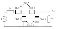
図2および3は、はしご型フィルタを形成する直列および並列FBARの配列を2種類示した概略図である。各フィルタは、直列に配列された2つのFBARと、並列に配列された2つのFBARを備えている。このようなフィルタは2×2はしご型フィルタという共通の名称で称され、ここで最初の数字は直列共振子の数を指し、二番目の数字は並列共振子の数を指す。ここでは便宜上、直列共振子をAで表し、並列共振子をBで表すこととする。直列共振子Aは、並列共振子Bとは面積と厚みが異なることも大いにありうる。直列共振子Aは全て同一であり、並列共振子Bも全て同一である。
【0035】
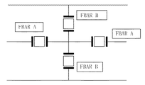
図2および3におけるFBARの配列は、接地順序において異なる。ここで、図2の配列をABABと称し、図3の配列をABBAと称する。これらの用語は直列共振子と並列共振子の順序を表すものである。
【0036】
図3に示されるABBAコプレーナ構成の2×2フィルタの実現例を、圧電層23がZnOからなる場合に適した寸法で図4A〜Dに示し、図2に示されるABABコプレーナ構成の2×2フィルタの実現例を図5A〜Dに示す。
【0037】
直列FBAR10および並列FBAR11は単一の膜構造上に配置されている。本発明によれば、工程が非常に簡素化され、ZnOからなる圧電層23をエッチングによりパターニングする必要がなくなる。コプレーナ伝送線路内においてABBA構成の場合もABAB構成の場合も、その2×2フィルタを構成する4つ全部のFBARに対し、一つの層によって下部電極25が形成される。
【0038】
CPW内でABBA構成のフィルタを用いると、例えばABBABBA(3/4)やABBABBAA(4/4)といったように、並列FBARの数が直列FBARの数以上となる、ある次数のはしご型フィルタをCPW内に形成することがより容易になる。
【0039】
単純なCPW内におけるABAB構成のフィルタの場合には、エッチングにより圧電メサを形成しないことには、ABABAB(3/3)のように直列FBARと並列FBARが同数のフィルタを作製することは困難である。一つのFBARにおいて、次のFBARの下部電極を形成できるように上部電極の金属パターンを圧電材料側にまで伸ばすには、メサが必要である。圧電材料をエッチングせずに作製できるのは、ABAAB(3/2)のように並列FBARの数が直列FBARよりも少ないフィルタだけである。
【0040】
ABBA構造は、他の導波路構成、例えばマイクロストリップなどにおいても使用できるが、ABAB構成で使用するよりもフィルタの占める面積が大きくなる。マイクロストリップ内のABBAフィルタの場合、圧電材料上の上部電極を次のFBARの下部電極に接続できるようにする電極の伝送構成のためには、圧電メサをエッチングしたり、エアブリッジ技術を用いたりすることが必要になる。
【0041】
図4に示されるABBA構成に配列された4つのFBARを包含するフィルタにおける上部表面の作製順序を説明する。まず、下部電極25のメタライズパターンを従来の作製技術によって規定する。そして圧電層23を全面に堆積させる。
【0042】
そして、従来技術にしたがい、直列FBARと並列FBARにそれぞれ異なる金属の厚み、およびそれによって異なる周波数を要求するかどうかに応じて、上部電極24の1つあるいは2つのメタライズパターンを堆積することにより、フィルタを完成する。
【0043】
作製の最終工程は、当業者に周知のバルクシリコンエッチングあるいは深い反応性エッチングといった技術により、絶縁層22の下に開口部28を形成することである。
【0044】
図5に示されるABABフィルタの作製工程は、層の作製順序が異なるがABBA構成の場合と同様である。
【0045】
ABAB構成およびABBA構成の、ZnOを用いた2×2FBARフィルタの透過係数(S21)を図6A,6Bで比較している。これらフィルタは挿入損失が同じで、帯域外減衰にほとんど差異はない。ABAB構成のほうが、ABBA構成よりも帯域端減衰極が深く、ロールオフが急峻で、帯域幅がわずかに広い。ABBA構造は、通過帯域がより平坦になりうる。
【0046】
強誘電性でもあり、従って分極処理が必要な圧電層23を用いた、本発明の2×2はしご型フィルタの更なる実施形態を図7A〜Dに示す。その作製手順は、共通の下部電極25にコンタクトホール26を形成することを除き、上述したZnOによるFBARフィルタの作製手順と同じである。このコンタクトホール26を使えば、ABBA構成において分極処理を行う際、共通の下部電極25への接続が可能になり、一つのフィルタ上で多数の下部電極を接続することが不要になる。ABAB構成の場合は、分極処理のための追加のコンタクトホールが必要となる。
【図面の簡単な説明】
【図1】
図1(A)は、FBARの上面図である。
図1(B)は、図1(A)に示したFBARの断面図である。
【図2】
図2は、ABABはしご型フィルタの概要図である。
【図3】
図3は、ABBAはしご型フィルタの概要図である。
【図4A】
図4Aは、図3に示したABBA構成を有する本発明の第1の実施形態に係るはしご型フィルタの上面図である。
【図4B】
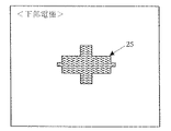
図4Bは、図4Aに示したABBAはしご型フィルタの下部電極を示している。
【図4C】
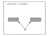
図4Cは、図4Aに示したABBAはしご型フィルタにおける並列FBARの上部電極を示している。
【図4D】
図4Dは、図4Aに示したABBAはしご型フィルタにおける直列FBARの上部電極を示している。
【図5A】
図5Aは、図2に示したABAB構成を有する本発明の第2の実施形態に係るはしご型フィルタの上面図である。
【図5B】
図5Bは、図5Aに示したABABはしご型フィルタの下部電極を示している。
【図5C】
図5Cは、図5Aに示したABABはしご型フィルタにおける並列FBARの上部電極を示している。
【図5D】
図5Dは、図5Aに示したABABはしご型フィルタにおける直列FBARの上部電極を示している。
【図6A】
図6Aは、図4および図5に示したABABおよびABBAはしご型フィルタのSパラメータの比較モデルを示している。
【図6B】
図6Bは、図4および図5に示したABABおよびABBAはしご型フィルタのSパラメータの比較モデルを示している。
【図7A】
図7Aは、本発明の第3の実施形態に係る、強誘電層を備えた図4と類似のABBAはしご型フィルタの上面図である。
【図7B】
図7Bは、図7Aに示したABBAはしご型フィルタの下部電極を示している。
【図7C】
図7Cは、図7Aに示したABBAはしご型フィルタにおける並列FBARの上部電極を示している。
【図7D】
図7Dは、図7Aに示したABBAはしご型フィルタにおける直列FBARの上部電極を示している。[0001]
The present invention relates to a filter or an improvement related to the filter, and more particularly to a thin film bulk acoustic wave resonator (FBAR) filter, and more particularly to an FBAR filter operating at microwave frequencies that can be easily manufactured using thin film technology. The improvements related to the configuration of
[0002]
It is important to prepare a filter at a high frequency in the MHz or GHz range. This is because today these frequency ranges are frequently used for wireless communication. For such applications, it is important that the size of the filter be as small as possible. Therefore, a filter configuration that can minimize the size of the filter on the substrate surface is desired.
[0003]
FBARs are attractive devices because they exhibit resonance peaks at high frequencies, especially in the MHz and GHz ranges. In addition, FBARs can be small devices (100100 micron size). Therefore, it is considered that the FBAR is also useful for mounting on a small, lightweight, thin electric appliance such as a mobile phone.
[0004]
FBARs typically combine a thin film piezoelectric layer, such as zinc oxide (ZnO), aluminum nitride (AlN) or lead zirconate titanate (PZT), with a thin film formed on a semiconductor substrate or a quarter wave acoustic stack. It is made by depositing on top. This combination forms an acoustic structure that resonates at a particular frequency.
[0005]
Conventional FBAR devices are connected to associated circuitry by contact pads and wire bonds. In this method, the ground connection is insufficient due to the parasitic inductance of the metal conductor. Also, this technique makes simulation and analysis of results difficult.
[0006]
An alternative method of incorporating the FBAR in a coplanar waveguide (CPW) structure requires a signal connection at the ground-signal-ground connection that contacts the top and bottom of the piezoelectric layer. In a known arrangement, the electrodes are separated from the transmission line structure. This increases the area and limits the size of devices that can be manufactured.
[0007]
The present invention seeks to overcome or mitigate the disadvantages of existing FBARs and to enable more compact filter configurations while having multiple FBARs.
[0008]
A preferred object of the present invention is to provide a filter with a plurality of FBARs, and in particular, a piezoelectric filter manufactured using thin film technology to minimize the planar area of the filter area on the wafer surface. is there.
[0009]
Yet another preferred object of the present invention is to provide a filter comprising a plurality of FBARs which is compact and exhibits a lower band edge attenuation pole (close-in rejection) and a lower out-of-band attenuation (out-of-band rejection). It is to be.
[0010]
These and other objects of the present invention are broadly achieved by arranging FBAR devices in a coplanar waveguide structure in which electrodes are incorporated within a coplanar transmission line.
[0011]
Thus, according to one aspect of the invention, there is provided an electrical filter comprising a plurality of FBARs comprising a thin layer of piezoelectric material sandwiched between two metal layers, wherein the electrodes of the series FBARs are in a transmission line of a coplanar waveguide. An electrical filter is provided wherein the FBARs are connected in a series and parallel connection arrangement such that the FBARs are part of a signal line and the electrodes of a parallel FBAR are connected to one or both sides of a grounded coplanar transmission line.
[0012]
By configuring the filter as a CPW structure, a small filter that is not affected by the floating parasitic effect can be obtained. Further, by incorporating the filter within the coplanar transmission line structure, wire bonding is not required, thereby simplifying manufacturing.
[0013]
The filter is preferably a ladder filter in which the series FBARs form one group and the parallel FBARs form another group. An advantage of the ladder filter configuration is that it does not require additional passive capacitance or inductor occupying extra area. In general, for a bandpass filter, the more FBARs used in the filter, the better the attenuation level compared to the signal passband.
[0014]
Typically, both the area and the thickness of the series FBAR and the parallel FBAR may be different, but the series FBAR has the same area and thickness, and the parallel FBAR also has the same area and thickness. The same series FBAR is referred to as an “A” type FBAR, and the same parallel FBAR is referred to as a “B” type FBAR.
[0015]
The serial and parallel FBARs may be arranged in the order ABAB or ABBA. Since the ABAB configuration occupies a larger area in the CPW structure than the ABBA configuration, the adoption of the ABBA configuration makes it possible to sufficiently utilize the device area.
[0016]
The ABBA configuration in the CPW is also suitable for simplifying the manufacture of small filters using thin-film technology, making it possible to easily manufacture higher-order filters without patterning the piezoelectric layer. I do.
[0017]
The FBAR may be disposed on the edge of the piezoelectric layer without forming an air bridge or a metal line.
[0018]
The piezoelectric material is advantageously chosen from zinc oxide, aluminum nitride, lead zirconate titanate, lead scandium tantalate and sodium bismuth titanate.
[0019]
Preferably, a connection to an electrode for polarizing the ferroelectric FBAR filter is provided.
[0020]
According to another aspect of the invention, the upper electrode of each series FBAR forms a part of the signal line of the coplanar waveguide structure, and the upper electrode of each parallel FBAR forms a part of the ground line of the coplanar waveguide structure. A ladder filter with FBARs arranged in series and parallel in a coplanar waveguide structure is provided.
[0021]
Preferably, the signal line is located between two ground lines.
[0022]
The FBARs of the filters according to the two sides of the invention advantageously have a common lower electrode.
[0023]
According to a further aspect of the invention, there is provided a ladder filter comprising a plurality of FBARs arranged in series and in parallel in a coplanar waveguide structure, wherein the FBAR is formed as part of a transmission line of the coplanar waveguide structure. There is provided a ladder filter having an electrode provided.
[0024]
According to yet a further aspect of the present invention, there is provided a ladder filter comprising a plurality of FBARs arranged in series and in parallel in a coplanar waveguide structure, wherein the FBAR formed on a substrate has the FBAR formed on the substrate. A ladder filter is provided that is connected to associated circuitry by one or more formed transmission lines.
[0025]
In accordance with yet another aspect of the present invention, there is provided a ladder filter comprising a plurality of FBARs in a series and parallel configuration included in a transmission line structure of a coplanar waveguide.
[0026]
Embodiments of the present invention will now be described in more detail, by way of example only, with reference to the accompanying drawings.
[0027]
Referring first to FIGS. 1A and 1B, a top view and a cross-sectional view of a standard FBAR are shown. The FBAR is arranged on the ground-signal-ground line signal line in the coplanar transmission line.
[0028]
The device is configured for two-port measurement, where a ground probe can be placed on either end of the
[0029]
The dimensions of the coplanar transmission line are designed to provide an environment of 50 ohms to this system, but minimize the overall size of the FBARs and FBAR filters while accommodating different areas of the FBARs and ground lines and signal lines. The design has sufficient flexibility so that the distance from the track can be changed.
[0030]
The FBAR consists of a continuous
[0031]
An overlapping region of the signal line defined on the insulating layer 22 and the signal line portion defined above the
[0032]
The output transmission line extends to the measurement point or other FBAR arranged in a ladder configuration. Since a continuous piezoelectric thin film is used, an input electrode and an output electrode must be defined before and after the deposition of the piezoelectric thin film. When manufacturing the
[0033]
The connection of the FBAR to the
[0034]
FIGS. 2 and 3 are schematic diagrams showing two types of arrangements of series and parallel FBARs forming a ladder filter. Each filter has two FBARs arranged in series and two FBARs arranged in parallel. Such filters are referred to by the
[0035]
The arrangement of the FBARs in FIGS. 2 and 3 differs in grounding order. Here, the array of FIG. 2 is called ABAB, and the array of FIG. 3 is called ABBA. These terms describe the order of the series resonator and the parallel resonator.
[0036]
FIGS. 4A to 4D show implementation examples of the 2 × 2 filter having the ABBA coplanar configuration shown in FIG. 3 with dimensions suitable for the case where the
[0037]
The
[0038]
When a filter having an ABBA configuration is used in the CPW, a ladder filter of a certain order in which the number of parallel FBARs is equal to or larger than the number of serial FBARs, such as ABBABBA (3/4) or ABBABBAA (4/4), is used as a CPW. It is easier to form in it.
[0039]
In the case of a filter having an ABAB configuration in a simple CPW, it is difficult to form a filter having the same number of series FBARs and parallel FBARs as ABABAB (3/3) without forming a piezoelectric mesa by etching. is there. In one FBAR, a mesa is required to extend the metal pattern of the upper electrode to the piezoelectric material side so that the lower electrode of the next FBAR can be formed. Only a filter such as ABAAB (3/2), which has a smaller number of parallel FBARs than a series FBAR, can be manufactured without etching the piezoelectric material.
[0040]
The ABBA structure can be used in other waveguide configurations, such as microstrips, but the filter occupies a larger area than is used in the ABAB configuration. In the case of an ABBA filter in a microstrip, the piezo mesas may be etched or air bridge technology may be used to transmit the electrodes so that the upper electrode on the piezoelectric material can be connected to the lower electrode of the next FBAR. Need to be done.
[0041]
The fabrication sequence of the top surface in a filter including four FBARs arranged in an ABBA configuration shown in FIG. 4 will be described. First, a metallized pattern of the
[0042]
Then, according to the prior art, depending on whether the series FBAR and the parallel FBAR require different metal thicknesses and thus different frequencies, by depositing one or two metallization patterns of the
[0043]
The final step in the fabrication is to form an
[0044]
The manufacturing process of the ABAB filter shown in FIG. 5 is the same as the case of the ABBA configuration, although the manufacturing order of the layers is different.
[0045]
6A and 6B compare the transmission coefficient (S 21 ) of the 2 × 2 FBAR filter using ZnO in the ABAB configuration and the ABBA configuration. These filters have the same insertion loss and little difference in out-of-band attenuation. The ABAB configuration has a deeper band edge attenuation pole, a steeper roll-off, and a slightly wider bandwidth than the ABBA configuration. The ABBA structure can have a flatter passband.
[0046]
A further embodiment of the 2 × 2 ladder filter of the present invention using a
[Brief description of the drawings]
FIG.
FIG. 1A is a top view of the FBAR.
FIG. 1B is a cross-sectional view of the FBAR shown in FIG.
FIG. 2
FIG. 2 is a schematic diagram of an ABAB ladder filter.
FIG. 3
FIG. 3 is a schematic diagram of an ABBA ladder filter.
FIG. 4A
FIG. 4A is a top view of the ladder filter according to the first embodiment of the present invention having the ABBA configuration shown in FIG.
FIG. 4B
FIG. 4B shows the lower electrode of the ABBA ladder filter shown in FIG. 4A.
FIG. 4C
FIG. 4C shows the upper electrode of the parallel FBAR in the ABBA ladder filter shown in FIG. 4A.
FIG. 4D
FIG. 4D shows the upper electrode of the series FBAR in the ABBA ladder filter shown in FIG. 4A.
FIG. 5A
FIG. 5A is a top view of a ladder filter according to the second embodiment of the present invention having the ABAB configuration shown in FIG.
FIG. 5B
FIG. 5B shows the lower electrode of the ABAB ladder filter shown in FIG. 5A.
FIG. 5C
FIG. 5C shows the upper electrode of the parallel FBAR in the ABAB ladder filter shown in FIG. 5A.
FIG. 5D
FIG. 5D shows the upper electrode of the series FBAR in the ABAB ladder filter shown in FIG. 5A.
FIG. 6A
FIG. 6A shows a comparison model of the S-parameters of the ABAB and ABBA ladder filters shown in FIGS. 4 and 5.
FIG. 6B
FIG. 6B shows a comparison model of the S-parameters of the ABAB and ABBA ladder filters shown in FIGS. 4 and 5.
FIG. 7A
FIG. 7A is a top view of an ABBA ladder filter similar to FIG. 4 with a ferroelectric layer according to a third embodiment of the present invention.
FIG. 7B
FIG. 7B shows the lower electrode of the ABBA ladder filter shown in FIG. 7A.
FIG. 7C
FIG. 7C shows the upper electrode of the parallel FBAR in the ABBA ladder filter shown in FIG. 7A.
FIG. 7D
FIG. 7D shows the upper electrode of the series FBAR in the ABBA ladder filter shown in FIG. 7A.
Claims (16)
Applications Claiming Priority (2)
| Application Number | Priority Date | Filing Date | Title |
|---|---|---|---|
| GBGB0029090.8A GB0029090D0 (en) | 2000-11-29 | 2000-11-29 | Improvements in or relating to filters |
| PCT/GB2001/003141 WO2002045265A1 (en) | 2000-11-29 | 2001-07-11 | Improvements in or relating to filters |
Related Child Applications (1)
| Application Number | Title | Priority Date | Filing Date |
|---|---|---|---|
| JP2003316522A Division JP2004007847A (en) | 2000-11-29 | 2003-09-09 | Thin film bulk wave resonator filter |
Publications (1)
| Publication Number | Publication Date |
|---|---|
| JP2004515149A true JP2004515149A (en) | 2004-05-20 |
Family
ID=9904094
Family Applications (2)
| Application Number | Title | Priority Date | Filing Date |
|---|---|---|---|
| JP2002546291A Withdrawn JP2004515149A (en) | 2000-11-29 | 2001-07-11 | Improvements in or related to filters |
| JP2003316522A Withdrawn JP2004007847A (en) | 2000-11-29 | 2003-09-09 | Thin film bulk wave resonator filter |
Family Applications After (1)
| Application Number | Title | Priority Date | Filing Date |
|---|---|---|---|
| JP2003316522A Withdrawn JP2004007847A (en) | 2000-11-29 | 2003-09-09 | Thin film bulk wave resonator filter |
Country Status (7)
| Country | Link |
|---|---|
| US (2) | US7187254B2 (en) |
| EP (1) | EP1340315B1 (en) |
| JP (2) | JP2004515149A (en) |
| AU (1) | AU2001269334A1 (en) |
| DE (1) | DE60131888T2 (en) |
| GB (1) | GB0029090D0 (en) |
| WO (1) | WO2002045265A1 (en) |
Families Citing this family (66)
| Publication number | Priority date | Publication date | Assignee | Title |
|---|---|---|---|---|
| GB0029090D0 (en) * | 2000-11-29 | 2001-01-10 | Univ Cranfield | Improvements in or relating to filters |
| US20040027030A1 (en) * | 2002-08-08 | 2004-02-12 | Li-Peng Wang | Manufacturing film bulk acoustic resonator filters |
| JP4128836B2 (en) * | 2002-09-27 | 2008-07-30 | Tdk株式会社 | Thin film piezoelectric resonator, filter and duplexer using the same |
| US7275292B2 (en) | 2003-03-07 | 2007-10-02 | Avago Technologies Wireless Ip (Singapore) Pte. Ltd. | Method for fabricating an acoustical resonator on a substrate |
| JP4024741B2 (en) * | 2003-10-20 | 2007-12-19 | 富士通メディアデバイス株式会社 | Piezoelectric thin film resonator and filter |
| US7332985B2 (en) * | 2003-10-30 | 2008-02-19 | Avago Technologies Wireless Ip (Singapore) Pte Ltd. | Cavity-less film bulk acoustic resonator (FBAR) devices |
| US6946928B2 (en) * | 2003-10-30 | 2005-09-20 | Agilent Technologies, Inc. | Thin-film acoustically-coupled transformer |
| US7019605B2 (en) * | 2003-10-30 | 2006-03-28 | Larson Iii John D | Stacked bulk acoustic resonator band-pass filter with controllable pass bandwidth |
| US7391285B2 (en) * | 2003-10-30 | 2008-06-24 | Avago Technologies Wireless Ip Pte Ltd | Film acoustically-coupled transformer |
| JP4223428B2 (en) * | 2004-03-31 | 2009-02-12 | 富士通メディアデバイス株式会社 | Filter and manufacturing method thereof |
| US7388454B2 (en) * | 2004-10-01 | 2008-06-17 | Avago Technologies Wireless Ip Pte Ltd | Acoustic resonator performance enhancement using alternating frame structure |
| US8981876B2 (en) * | 2004-11-15 | 2015-03-17 | Avago Technologies General Ip (Singapore) Pte. Ltd. | Piezoelectric resonator structures and electrical filters having frame elements |
| US7202560B2 (en) | 2004-12-15 | 2007-04-10 | Avago Technologies Wireless Ip (Singapore) Pte. Ltd. | Wafer bonding of micro-electro mechanical systems to active circuitry |
| US7791434B2 (en) * | 2004-12-22 | 2010-09-07 | Avago Technologies Wireless Ip (Singapore) Pte. Ltd. | Acoustic resonator performance enhancement using selective metal etch and having a trench in the piezoelectric |
| US7427819B2 (en) * | 2005-03-04 | 2008-09-23 | Avago Wireless Ip Pte Ltd | Film-bulk acoustic wave resonator with motion plate and method |
| US7369013B2 (en) * | 2005-04-06 | 2008-05-06 | Avago Technologies Wireless Ip Pte Ltd | Acoustic resonator performance enhancement using filled recessed region |
| US7436269B2 (en) * | 2005-04-18 | 2008-10-14 | Avago Technologies Wireless Ip (Singapore) Pte. Ltd. | Acoustically coupled resonators and method of making the same |
| US7934884B2 (en) * | 2005-04-27 | 2011-05-03 | Lockhart Industries, Inc. | Ring binder cover |
| KR100622393B1 (en) * | 2005-07-05 | 2006-09-12 | 삼성전자주식회사 | Bulk acoustic resonator comprising a resonance part with dimple and fabrication method therefor |
| US7868522B2 (en) | 2005-09-09 | 2011-01-11 | Avago Technologies Wireless Ip (Singapore) Pte. Ltd. | Adjusted frequency temperature coefficient resonator |
| US7391286B2 (en) * | 2005-10-06 | 2008-06-24 | Avago Wireless Ip Pte Ltd | Impedance matching and parasitic capacitor resonance of FBAR resonators and coupled filters |
| US7425787B2 (en) * | 2005-10-18 | 2008-09-16 | Avago Technologies Wireless Ip (Singapore) Pte. Ltd. | Acoustic galvanic isolator incorporating single insulated decoupled stacked bulk acoustic resonator with acoustically-resonant electrical insulator |
| US7525398B2 (en) * | 2005-10-18 | 2009-04-28 | Avago Technologies General Ip (Singapore) Pte. Ltd. | Acoustically communicating data signals across an electrical isolation barrier |
| US7675390B2 (en) * | 2005-10-18 | 2010-03-09 | Avago Technologies Wireless Ip (Singapore) Pte. Ltd. | Acoustic galvanic isolator incorporating single decoupled stacked bulk acoustic resonator |
| US7737807B2 (en) | 2005-10-18 | 2010-06-15 | Avago Technologies Wireless Ip (Singapore) Pte. Ltd. | Acoustic galvanic isolator incorporating series-connected decoupled stacked bulk acoustic resonators |
| US7423503B2 (en) * | 2005-10-18 | 2008-09-09 | Avago Technologies Wireless Ip (Singapore) Pte. Ltd. | Acoustic galvanic isolator incorporating film acoustically-coupled transformer |
| US7463499B2 (en) * | 2005-10-31 | 2008-12-09 | Avago Technologies General Ip (Singapore) Pte Ltd. | AC-DC power converter |
| US7561009B2 (en) * | 2005-11-30 | 2009-07-14 | Avago Technologies General Ip (Singapore) Pte. Ltd. | Film bulk acoustic resonator (FBAR) devices with temperature compensation |
| US7612636B2 (en) * | 2006-01-30 | 2009-11-03 | Avago Technologies Wireless Ip (Singapore) Pte. Ltd. | Impedance transforming bulk acoustic wave baluns |
| US20070210724A1 (en) * | 2006-03-09 | 2007-09-13 | Mark Unkrich | Power adapter and DC-DC converter having acoustic transformer |
| US7746677B2 (en) * | 2006-03-09 | 2010-06-29 | Avago Technologies Wireless Ip (Singapore) Pte. Ltd. | AC-DC converter circuit and power supply |
| US7479685B2 (en) * | 2006-03-10 | 2009-01-20 | Avago Technologies General Ip (Singapore) Pte. Ltd. | Electronic device on substrate with cavity and mitigated parasitic leakage path |
| US7851709B2 (en) * | 2006-03-22 | 2010-12-14 | Advanced Semiconductor Engineering, Inc. | Multi-layer circuit board having ground shielding walls |
| US7508286B2 (en) * | 2006-09-28 | 2009-03-24 | Avago Technologies Wireless Ip (Singapore) Pte. Ltd. | HBAR oscillator and method of manufacture |
| US20080202239A1 (en) * | 2007-02-28 | 2008-08-28 | Fazzio R Shane | Piezoelectric acceleration sensor |
| US20090079514A1 (en) * | 2007-09-24 | 2009-03-26 | Tiberiu Jamneala | Hybrid acoustic resonator-based filters |
| US7791435B2 (en) * | 2007-09-28 | 2010-09-07 | Avago Technologies Wireless Ip (Singapore) Pte. Ltd. | Single stack coupled resonators having differential output |
| US7732977B2 (en) * | 2008-04-30 | 2010-06-08 | Avago Technologies Wireless Ip (Singapore) | Transceiver circuit for film bulk acoustic resonator (FBAR) transducers |
| US7855618B2 (en) * | 2008-04-30 | 2010-12-21 | Avago Technologies Wireless Ip (Singapore) Pte. Ltd. | Bulk acoustic resonator electrical impedance transformers |
| US7888843B2 (en) * | 2008-09-10 | 2011-02-15 | Georgia Tech Research Corporation | Thin-film piezoelectric-on-insulator resonators having perforated resonator bodies therein |
| US7834524B2 (en) * | 2009-01-30 | 2010-11-16 | Integrated Device Technology, Inc. | Micro-electromechanical devices having variable capacitors therein that compensate for temperature-induced frequency drift in acoustic resonators |
| US7939990B2 (en) * | 2009-01-30 | 2011-05-10 | Integrated Device Technology, Inc. | Thin-film bulk acoustic resonators having perforated bodies that provide reduced susceptibility to process-induced lateral dimension variations |
| US8291559B2 (en) * | 2009-02-24 | 2012-10-23 | Epcos Ag | Process for adapting resonance frequency of a BAW resonator |
| EP2443745A1 (en) * | 2009-06-19 | 2012-04-25 | Georgia Tech Research Corporation | Methods of forming micromechanical resonators having high density trench arrays therein that provide passive temperature compensation |
| US8902023B2 (en) * | 2009-06-24 | 2014-12-02 | Avago Technologies General Ip (Singapore) Pte. Ltd. | Acoustic resonator structure having an electrode with a cantilevered portion |
| US8248185B2 (en) * | 2009-06-24 | 2012-08-21 | Avago Technologies Wireless Ip (Singapore) Pte. Ltd. | Acoustic resonator structure comprising a bridge |
| US8106724B1 (en) | 2009-07-23 | 2012-01-31 | Integrated Device Technologies, Inc. | Thin-film bulk acoustic resonators having perforated resonator body supports that enhance quality factor |
| US8193877B2 (en) * | 2009-11-30 | 2012-06-05 | Avago Technologies Wireless Ip (Singapore) Pte. Ltd. | Duplexer with negative phase shifting circuit |
| US8796904B2 (en) | 2011-10-31 | 2014-08-05 | Avago Technologies General Ip (Singapore) Pte. Ltd. | Bulk acoustic resonator comprising piezoelectric layer and inverse piezoelectric layer |
| US9243316B2 (en) | 2010-01-22 | 2016-01-26 | Avago Technologies General Ip (Singapore) Pte. Ltd. | Method of fabricating piezoelectric material with selected c-axis orientation |
| US8962443B2 (en) | 2011-01-31 | 2015-02-24 | Avago Technologies General Ip (Singapore) Pte. Ltd. | Semiconductor device having an airbridge and method of fabricating the same |
| US8501515B1 (en) | 2011-02-25 | 2013-08-06 | Integrated Device Technology Inc. | Methods of forming micro-electromechanical resonators using passive compensation techniques |
| US9148117B2 (en) | 2011-02-28 | 2015-09-29 | Avago Technologies General Ip (Singapore) Pte. Ltd. | Coupled resonator filter comprising a bridge and frame elements |
| US9136818B2 (en) | 2011-02-28 | 2015-09-15 | Avago Technologies General Ip (Singapore) Pte. Ltd. | Stacked acoustic resonator comprising a bridge |
| US9203374B2 (en) | 2011-02-28 | 2015-12-01 | Avago Technologies General Ip (Singapore) Pte. Ltd. | Film bulk acoustic resonator comprising a bridge |
| US9083302B2 (en) | 2011-02-28 | 2015-07-14 | Avago Technologies General Ip (Singapore) Pte. Ltd. | Stacked bulk acoustic resonator comprising a bridge and an acoustic reflector along a perimeter of the resonator |
| US9154112B2 (en) | 2011-02-28 | 2015-10-06 | Avago Technologies General Ip (Singapore) Pte. Ltd. | Coupled resonator filter comprising a bridge |
| US9425764B2 (en) | 2012-10-25 | 2016-08-23 | Avago Technologies General Ip (Singapore) Pte. Ltd. | Accoustic resonator having composite electrodes with integrated lateral features |
| US9048812B2 (en) | 2011-02-28 | 2015-06-02 | Avago Technologies General Ip (Singapore) Pte. Ltd. | Bulk acoustic wave resonator comprising bridge formed within piezoelectric layer |
| US8575820B2 (en) | 2011-03-29 | 2013-11-05 | Avago Technologies General Ip (Singapore) Pte. Ltd. | Stacked bulk acoustic resonator |
| US9444426B2 (en) | 2012-10-25 | 2016-09-13 | Avago Technologies General Ip (Singapore) Pte. Ltd. | Accoustic resonator having integrated lateral feature and temperature compensation feature |
| US8350445B1 (en) | 2011-06-16 | 2013-01-08 | Avago Technologies Wireless Ip (Singapore) Pte. Ltd. | Bulk acoustic resonator comprising non-piezoelectric layer and bridge |
| US8922302B2 (en) | 2011-08-24 | 2014-12-30 | Avago Technologies General Ip (Singapore) Pte. Ltd. | Acoustic resonator formed on a pedestal |
| US8610336B1 (en) | 2011-09-30 | 2013-12-17 | Integrated Device Technology Inc | Microelectromechanical resonators having resistive heating elements therein configured to provide frequency tuning through convective heating of resonator bodies |
| EP3229359A1 (en) * | 2016-04-06 | 2017-10-11 | Neumüller Elektronik GmbH | Resonant converter and power device with such a converter |
| DE112019004743T5 (en) * | 2018-09-21 | 2021-06-02 | Murata Manufacturing Co., Ltd. | Piezoelectric component |
Family Cites Families (18)
| Publication number | Priority date | Publication date | Assignee | Title |
|---|---|---|---|---|
| US5185589A (en) * | 1991-05-17 | 1993-02-09 | Westinghouse Electric Corp. | Microwave film bulk acoustic resonator and manifolded filter bank |
| US5382930A (en) * | 1992-12-21 | 1995-01-17 | Trw Inc. | Monolithic multipole filters made of thin film stacked crystal filters |
| JP3181475B2 (en) * | 1994-08-12 | 2001-07-03 | ティーディーケイ株式会社 | Surface acoustic wave device |
| US6051907A (en) * | 1996-10-10 | 2000-04-18 | Nokia Mobile Phones Limited | Method for performing on-wafer tuning of thin film bulk acoustic wave resonators (FBARS) |
| US5872493A (en) | 1997-03-13 | 1999-02-16 | Nokia Mobile Phones, Ltd. | Bulk acoustic wave (BAW) filter having a top portion that includes a protective acoustic mirror |
| US5910756A (en) | 1997-05-21 | 1999-06-08 | Nokia Mobile Phones Limited | Filters and duplexers utilizing thin film stacked crystal filter structures and thin film bulk acoustic wave resonators |
| US5932953A (en) * | 1997-06-30 | 1999-08-03 | Iowa State University Research Foundation, Inc. | Method and system for detecting material using piezoelectric resonators |
| US5854579A (en) * | 1997-08-25 | 1998-12-29 | Motorola Inc. | Saw filter using low-pass configuration and method of providing the same |
| US6081171A (en) | 1998-04-08 | 2000-06-27 | Nokia Mobile Phones Limited | Monolithic filters utilizing thin film bulk acoustic wave devices and minimum passive components for controlling the shape and width of a passband response |
| US5942958A (en) * | 1998-07-27 | 1999-08-24 | Tfr Technologies, Inc. | Symmetrical piezoelectric resonator filter |
| US6262637B1 (en) * | 1999-06-02 | 2001-07-17 | Agilent Technologies, Inc. | Duplexer incorporating thin-film bulk acoustic resonators (FBARs) |
| US6720842B2 (en) * | 2000-02-14 | 2004-04-13 | Murata Manufacturing Co., Ltd. | Surface acoustic wave filter device having first through third surface acoustic wave filter elements |
| GB0012437D0 (en) * | 2000-05-24 | 2000-07-12 | Univ Cranfield | Improvements to filters |
| GB0012439D0 (en) * | 2000-05-24 | 2000-07-12 | Univ Cranfield | Improvements to filters |
| GB0029090D0 (en) * | 2000-11-29 | 2001-01-10 | Univ Cranfield | Improvements in or relating to filters |
| JP3949990B2 (en) * | 2002-03-29 | 2007-07-25 | 株式会社東芝 | Voltage controlled oscillator |
| TW540173B (en) * | 2002-05-03 | 2003-07-01 | Asia Pacific Microsystems Inc | Bulk acoustic device having integrated fine-tuning and trimming devices |
| JP4128836B2 (en) * | 2002-09-27 | 2008-07-30 | Tdk株式会社 | Thin film piezoelectric resonator, filter and duplexer using the same |
-
2000
- 2000-11-29 GB GBGB0029090.8A patent/GB0029090D0/en not_active Ceased
-
2001
- 2001-07-11 WO PCT/GB2001/003141 patent/WO2002045265A1/en active IP Right Grant
- 2001-07-11 EP EP01947689A patent/EP1340315B1/en not_active Expired - Lifetime
- 2001-07-11 AU AU2001269334A patent/AU2001269334A1/en not_active Abandoned
- 2001-07-11 JP JP2002546291A patent/JP2004515149A/en not_active Withdrawn
- 2001-07-11 DE DE60131888T patent/DE60131888T2/en not_active Expired - Lifetime
- 2001-07-11 US US10/380,985 patent/US7187254B2/en not_active Expired - Lifetime
-
2003
- 2003-09-09 JP JP2003316522A patent/JP2004007847A/en not_active Withdrawn
- 2003-11-24 US US10/718,799 patent/US7199504B2/en not_active Expired - Lifetime
Also Published As
| Publication number | Publication date |
|---|---|
| US7187254B2 (en) | 2007-03-06 |
| US7199504B2 (en) | 2007-04-03 |
| EP1340315A1 (en) | 2003-09-03 |
| DE60131888D1 (en) | 2008-01-24 |
| AU2001269334A1 (en) | 2002-06-11 |
| DE60131888T2 (en) | 2008-12-04 |
| US20040150295A1 (en) | 2004-08-05 |
| WO2002045265A1 (en) | 2002-06-06 |
| US20040061416A1 (en) | 2004-04-01 |
| EP1340315B1 (en) | 2007-12-12 |
| GB0029090D0 (en) | 2001-01-10 |
| JP2004007847A (en) | 2004-01-08 |
Similar Documents
| Publication | Publication Date | Title |
|---|---|---|
| JP2004515149A (en) | Improvements in or related to filters | |
| JP3996379B2 (en) | Filter structure and configuration including a piezoelectric resonator | |
| US6977563B2 (en) | Thin-film piezoelectric resonator and method for fabricating the same | |
| US5185589A (en) | Microwave film bulk acoustic resonator and manifolded filter bank | |
| US7128941B2 (en) | Method for fabricating film bulk acoustic resonator (FBAR) device | |
| JP4171214B2 (en) | Monolithic FBAR duplexer and method of making the same | |
| JP5296282B2 (en) | Bulk acoustic wave device | |
| US9450563B2 (en) | Acoustic wave bandpass filter comprising integrated acoustic guiding | |
| KR100771345B1 (en) | Piezoelectric thin-film resonator and filter | |
| KR20030035784A (en) | Piezoelectric thin film resonator, filter and manufacturing method of the piezoelectric thin film resonator | |
| JP2005057332A (en) | Filter apparatus and branching apparatus employing the same | |
| KR20190034838A (en) | Air-gap type fbar and method for fabricating by the same | |
| KR20050021309A (en) | Film bulk acoustic resonator and method of producing the same | |
| JP4791181B2 (en) | Thin film bulk acoustic wave resonator, filter and communication device including the same, and method for manufacturing thin film bulk acoustic wave resonator | |
| US7138888B2 (en) | Filter using piezoelectric resonator | |
| JP2005184851A (en) | Duplexer manufactured with integrated fbar and isolation part, and method of manufacturing the same | |
| JP3839492B2 (en) | Thin film piezoelectric element | |
| JP2018006919A (en) | Acoustic wave device | |
| US7078984B2 (en) | Duplexer and method of manufacturing same | |
| KR100393774B1 (en) | Manufacturing method for bandpass filter using thin film bulk acoustic resonator | |
| KR100429972B1 (en) | Manufacturing method for duplexer using thin film bulk acoustic resonator | |
| CN115242214A (en) | Manufacturing method of high-performance high-frequency thin-film mechanical wave resonator | |
| CN117439562A (en) | Radio frequency device, electronic equipment and manufacturing method | |
| KR20200073968A (en) | bulk-acoustic resonator and bulk-acoustic filter device |
Legal Events
| Date | Code | Title | Description |
|---|---|---|---|
| A621 | Written request for application examination |
Free format text: JAPANESE INTERMEDIATE CODE: A621 Effective date: 20080415 |
|
| A761 | Written withdrawal of application |
Free format text: JAPANESE INTERMEDIATE CODE: A761 Effective date: 20090309 |