JP2004363447A - Semiconductor device and method of manufacturing the same - Google Patents
Semiconductor device and method of manufacturing the same Download PDFInfo
- Publication number
- JP2004363447A JP2004363447A JP2003162042A JP2003162042A JP2004363447A JP 2004363447 A JP2004363447 A JP 2004363447A JP 2003162042 A JP2003162042 A JP 2003162042A JP 2003162042 A JP2003162042 A JP 2003162042A JP 2004363447 A JP2004363447 A JP 2004363447A
- Authority
- JP
- Japan
- Prior art keywords
- film
- semiconductor device
- wiring
- interlayer insulating
- gas
- Prior art date
- Legal status (The legal status is an assumption and is not a legal conclusion. Google has not performed a legal analysis and makes no representation as to the accuracy of the status listed.)
- Withdrawn
Links
Images


Abstract
Description
【0001】
【発明の属する技術分野】
本発明は半導体装置の製造方法に関し、より詳しくは、低誘電率絶縁膜を用いたダマシン法による半導体装置の製造方法に関する。
【0002】
【従来の技術】
近年、半導体デバイスの高速化は著しく、多層配線部における配線抵抗と配線間や配線層間の寄生容量に起因する信号伝搬速度の低下による伝送遅延が問題となってきている。こうした問題は、半導体デバイスの高集積化に伴う配線幅および配線間隔の微細化につれて配線抵抗が上昇し且つ寄生容量が増大するので、益々顕著となる傾向にある。
【0003】
配線抵抗および寄生容量の増大に基づく信号遅延を防止するために、従来より、アルミニウム配線に代わる銅配線の導入が行われるとともに、層間絶縁膜として低誘電率の絶縁膜(以下、Low−k膜という。)を用いることが試みられてきた。
【0004】
Low−k膜を用いた銅配線の形成方法としては、ダマシン法によるものがある。これは、銅がアルミニウムに比較してエッチングレートの制御が困難であることに鑑み、銅をエッチングせずに配線を形成する技術として知られている。
【0005】
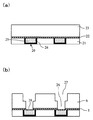
図6および図7を用いて、ダマシン法による従来の銅配線形成工程について説明する。
【0006】
まず、銅配線層20が形成されたシリコン基板21の上に、ストッパー膜22、Low−k膜23をこの順に形成して、図6(a)に示す構造とする。ここで、銅配線層20はバリアメタル膜24と銅層25とを有している。次に、Low−k膜23およびストッパー膜22をエッチングし、図6(b)に示すビアホール26および配線溝27を形成する。
【0007】
【発明が解決しようとする課題】
ビアホール26の形成によって露出した銅配線層20の表面には、酸化銅などの高抵抗層28が形成されている。従来は、アルゴンプラズマを用いた物理的エッチングによって高抵抗層28を除去していた。しかしながら、この方法では、高抵抗層28だけでなくビアホール26や配線溝27の内壁もエッチングされるために、開口面積が広がって、これらの断面形状がテーパ状になるという問題があった(図7(a))。特に、Low−k膜23として多孔質化膜を用いた場合、このような現象が顕著に見られるようになる。
【0008】
高抵抗層28を除去した後は、ビアホール26および配線溝27の内面にバリアメタル膜29を形成し、ビアホール26および配線溝27に銅層30を埋め込んで、ビアプラグ31および銅配線層32を形成する。以上の工程によって、シリコン基板21に形成された銅配線層20と上層の銅配線層32とがビアプラグ31を介して電気的に接続された銅配線が形成される(図7(b))。ここで、従来法によれば、ビアホール26および配線溝27の開口面積が大きくなるために、隣接する配線間の距離Rが短くなって短絡が生じるという問題があった。
【0009】
また、プラズマエッチングされた銅が、ビアホール26の側壁に付着するという問題もあった。付着した銅は、後工程での加熱によってLow−k膜23中を拡散し、配線間でのリーク電流を増大させることになる。
【0010】
さらには、アルゴンプラズマによってLow−k膜23がダメージを受ける結果、配線間での容量が増加したり、Low−k膜23が収縮して信頼性が低下したりするなどの問題もあった。
【0011】
本発明はこのような問題点に鑑みてなされたものである。即ち、本発明の目的は、ビアホールおよび配線溝の形状を変えることなしに高抵抗層を除去することのできる半導体装置の製造方法を提供することにある。
【0012】
また、本発明の目的は、高抵抗層を除去する際のビアホールや配線溝の内壁への銅の付着を防いで、リーク電流を低減させることのできる半導体装置の製造方法を提供することにある。
【0013】
さらに、本発明の目的は、プラズマダメージを受けにくいLow−k膜を使用することによって、電気的特性および信頼性に優れた半導体装置を提供することにある。
【0014】
本発明の他の目的および利点は、以下の記載から明らかとなるであろう。
【0015】
【課題を解決するための手段】
本発明は、金属配線を有する半導体装置であって、この金属配線上の層間絶縁膜は、ヤング率が7GPa以上で比誘電率が3未満であることを特徴とする。本発明において、金属配線は銅配線とすることができる。また、層間絶縁膜は、多孔質SiO2膜、SiOC膜、ポリアリルエーテル誘導体膜、フッ素化アリレン膜、PSG膜、BPSG膜、USG膜、FSG膜、PE−TEOS膜およびSOG膜よりなる群から選ばれるいずれか1の膜とすることができる。
【0016】
また、本発明は、金属配線を有する半導体装置の製造方法であって、この金属配線の上にストッパー膜を形成する工程と、このストッパー膜の上にヤング率が7GPa以上で比誘電率が3未満である層間絶縁膜を形成する工程と、この層間絶縁膜をエッチングしてストッパー膜に達する開口部を形成する工程と、この開口部に露出しているストッパー膜をエッチングすることによりビアホールを形成して金属配線を露出させる工程と、層間絶縁膜をエッチングして配線溝を形成する工程と、露出した金属配線の表面を還元性ガスでプラズマ処理する工程とを有することを特徴とする。
【0017】
本発明の半導体装置の製造方法において、還元性ガスは、水素、アンモニアおよびヒドラジンよりなる群から選ばれる少なくとも1のガスを含むことができる。
【0018】
また、本発明の半導体装置の製造方法において、還元性ガスは、5atom%以下の濃度の水素ガスを含むことができる。また、還元性ガスは、0.5atom%〜2atom%の濃度の水素ガスを含むことが好ましい。
【0019】
また、本発明の半導体装置の製造方法において、還元性ガスは、上記のガスに加えて、窒素、ヘリウム、ネオン、アルゴン、クリプトンおよびキセノンよりなる群から選ばれる少なくとも1のガスをさらに含むことができる。
【0020】
【発明の実施の形態】
以下、本発明の実施の形態を図面を参照しながら詳細に説明する。
【0021】
図1〜図3は、本実施の形態における半導体装置の製造方法を示す断面図である。
【0022】
まず、金属配線層としての銅配線層1が形成された半導体基板2を準備する。ここで、銅配線層1は、バリアメタル膜4および銅層5を有している。半導体基板2としては、例えばシリコン基板などを用いることができる。
【0023】
次に、半導体基板2の上にストッパー膜3を形成して、図1(a)に示す構造とする。ストッパー膜3は、上に形成される層間絶縁膜とのエッチング選択比が大きい材料を用いることが好ましい。具体的には、層間絶縁膜の種類に応じて適宜決定されるが、例えば、SiC膜、SixNy(例えば、Si3N4、Si2N3、SiNなど。)膜、SiCN膜またはSiOC膜などを用いることができる。これらの膜は、CVD(Chemical Vapor Deposition)法またはスパッタ法などによって成膜することができる。
【0024】
次に、ストッパー膜3の上に層間絶縁膜6を形成する(図1(b))。
【0025】
本発明において、層間絶縁膜6は、低誘電率の絶縁膜(以下、Low−k膜という。)であることが好ましく、比誘電率が3未満のLow−k膜であることがより好ましく、ヤング率が7GPa以上で比誘電率が3未満のLow−k膜であることが特に好ましい。層間絶縁膜の比誘電率を小さくすることによって、配線間容量を小さくして配線遅延時間の低減を図ることができる。また、ヤング率が7GPa以上の材料を用いることによって、耐プラズマ性に十分な機械的強度を有する層間絶縁膜とすることができる。
【0026】
比誘電率が3未満のLow−k膜としては、例えば、多孔質SiO2膜、SiOC膜、ポリアリルエーテル誘導体膜、フッ素化アリレン膜、PSG(リン含有ケイ酸塩ガラス)膜、BPSG(ホウ素リン含有ケイ酸塩ガラス)膜、USG(アンドープケイ酸塩ガラス)膜、FSG(フッ素ドープケイ酸塩ガラス)膜、PE−TEOS(Plasma Enhanced−tetra Ethyl Ortho Silicate)膜またはSOG(Spin on Glass)膜などを挙げることができる。さらに、SOG膜の材料としては、例えば、水素シルセスキオキサン(HSQ)またはメチルシルセスキオキサン(MSQ)などを挙げることができる。これらの膜は、CVD法、PVD(Physical Vapor Deposition)法またはSOD(Spin on Dielectric Coating)法などによって成膜することができる。
【0027】
また、Low−k膜のヤング率は、例えば、層間絶縁膜を構成する樹脂の骨格を変えたり、多孔質化材の大きさや量などを変えたりすることによって制御することができる。ヤング率が大きいほど膜の硬度は上昇することから、プラズマに対する耐性を向上させるためには、Low−k膜のヤング率は大きい方が好ましい。本発明者は、鋭意研究した結果、ヤング率が7GPa以上の値を有していれば、配線間容量の増加や膜収縮のレベルが実用上問題のない範囲に収まることを見出した。
【0028】
層間絶縁膜6を形成した後は、この上にハードマスク7を形成する(図1(b))。
【0029】
ハードマスク7は、後述するレジスト膜の形成の際に層間絶縁膜6がエッチングされるのを防ぐ役割を有する。ハードマスク7としては、例えば、CVD法またはスパッタ法などによって成膜された、SiO2膜またはSixNy(例えば、Si3N4、Si2N3、SiNなど。)膜などを用いることができる。
【0030】
ハードマスク7を形成した後は、この上に所定のパターンを有するレジスト膜8を形成して、図1(c)に示す構造とする。具体的には、ハードマスク7の上にフォトレジストを塗布した後、これを露光・現像することによってレジスト膜8を形成することができる。
【0031】
次に、レジスト膜8をマスクとして、ハードマスク7および層間絶縁膜6を異方性エッチングして開口部9を形成する。このエッチングは、ストッパー膜3に達した時点で自動的に停止する。そして、図2(a)に示すように、開口部9の底部にストッパー膜3の一部3aが露出する。
【0032】
エッチング装置としては、例えば、上部電極と下部電極にそれぞれ所定の高周波を印加することのできる2周波励起平行平板型リアクティブイオンエッチャーを用いることができる。また、エッチングガスとして、テトラフルオロメタン(CF4)、ヘキサフルオロブチン(C4F6)、オクタフルオロブテン(C4F8)、オクタフルオロペンチン(C5F8)、トリフルオロメタン(CHF3)およびジフルオロメタン(CH2F2)よりなる群から選ばれる少なくとも1種のガスと、エッチングガス以外の希釈ガスとして、ヘリウム(He)、アルゴン(Ar)、窒素(N2)、一酸化炭素(CO)および酸素(O2)よりなる群から選ばれる少なくとも1種のガスとを含む混合ガスを用いることができる。例えば、オクタフルオロブテン(C4F8)、窒素(N2)およびアルゴン(Ar)からなる混合ガスをエッチングガスとして装置内に導き、エッチングチャンバ内を所定の圧力に維持した状態で、上部電極と下部電極にそれぞれ所定の電力を印加してプラズマを発生させる。
【0033】
ハードマスク7および層間絶縁膜6のエッチングが終了した後は、不要となったレジスト膜8をアッシングにより除去する。例えば、酸素(O2)ガス、アンモニア(NH3)ガス、または窒素(N2)と水素(H2)との混合ガスなどを用いてアッシングを行うことができる。
【0034】
次に、開口部9に露出したストッパー膜3aのエッチングを行い、ビアホール10を形成する(図2(b))。例えば、上記の2周波励起平行平板型リアクティブイオンエッチャー内に、テトラフルオロメタン(CF4)と窒素(N2)との混合ガスを導き、エッチングチャンバ内を所定の圧力に維持した状態で、上部電極と下部電極にそれぞれ所定の電力を印加する。これにより発生したプラズマによって、ストッパー膜3aのエッチングを行うことができる。
【0035】
次に、フォトリソグラフィー法によってビアホール10の上に配線溝11を形成し、図2(c)に示す構造とする。
【0036】
図2(c)において、ビアホール10の底面には、下層の銅配線層1の表面が露出している。そして、この露出した銅配線層1の表面には、銅が雰囲気中の酸素と反応して生成した酸化銅を主成分とする高抵抗層12が形成される(図3(a))。高抵抗層12が存在したままで上層の銅配線層を形成すると、接触抵抗が増加して半導体装置の電気的特性を低下させることになる。そこで、ビアホール10および配線溝11を形成した後、図3(a)に示すようにして高抵抗層12の除去を行ってから、上層の銅配線層形成工程へと進む。
【0037】
本発明は、還元性のガスを用いた銅配線層1表面のプラズマ処理によって高抵抗層12を除去することを特徴としている。還元性のガスとしては、例えば、水素、アンモニアおよびヒドラジンよりなる群から選ばれる少なくとも1種のガスを用いることができる。また、還元性のガスと、これに不活性なガスとの混合ガスを用いてプラズマ処理を行ってもよい。還元性のガスに不活性なガスとしては、例えば、窒素(N2)、ヘリウム(He)、ネオン(Ne)、アルゴン(Ar)、クリプトン(Kr)およびキセノン(Xe)よりなる群から選ばれる少なくとも1種のガスを挙げることができる。酸素などの酸化性ガスがエッチングガス中に含まれると、還元性ガスと反応して還元作用が低下することから好ましくない。
【0038】
還元性ガスを用いてプラズマ処理を行うと、プラズマ中に発生した活性水素が銅配線層1の表面に吸着して酸化銅を銅に還元する。また、活性水素は、銅配線層1の表面に衝突して物理的エッチングも行う。エッチングガス中に不活性ガスが含まれている場合には、不活性ガスから生じた活性種による物理的エッチングも行われる。
【0039】
従来法による高抵抗層の除去では、アルゴンプラズマによる物理的エッチングのみが行われていた。これに対して、本発明では、高抵抗層の主成分である酸化銅を銅に還元する化学的エッチングと、活性種の衝突による物理的エッチングの両方を併用することを特徴としている。これにより、高抵抗層を効率的に除去することが可能となるので、配線溝およびビアホールの内壁へのエッチングを抑制するとともに、層間絶縁膜へ与えるダメージを低減させることが可能となる。また、銅への還元反応によって酸化銅を除去するので、物理的エッチングのみによって酸化銅を除去する場合に比べて、ビアホールおよび配線溝の内壁への銅の付着を低減させることができる。
【0040】
本発明においては、ビアホールおよび配線溝の内壁がエッチングされることによる配線間容量の増大が実用上問題ないレベルに収まるようにして、エッチングガス中に含まれる還元性ガスの濃度を決定することが望ましい。例えば、還元性ガスとして水素(H2)を含むガスを用いる場合、水素濃度が多くなりすぎると、配線溝およびビアホールの内壁のエッチング、並びにプラズマダメージによる層間絶縁膜の膜質変化がおこり、配線間容量が増大するようになる。したがって、実用上は、水素濃度が5atom%以下であることが好ましく、2atom%以下であることがより好ましい。一方、エッチングガス中に水素が存在することによって還元作用が認められるようになるが、水素濃度が低くなりすぎると、還元に時間を要してスループットが低下する。したがって、水素濃度の下限値は、0.5atom%以上であることが好ましい。
【0041】
高抵抗層12を除去した後は、ビアホール10および配線溝11の内面にバリアメタル膜13を形成し、バリアメタル膜13を介してこれらの内部に銅層14の埋込みを行うことによって、ビアプラグ15および銅配線層16を形成する(図3(b))。高抵抗層12の除去からバリアメタル膜13の形成までの工程は、連続して行うことが好ましい。具体的には、次のようにして行うことができる。
【0042】
高抵抗層12を除去した後、同一のチャンバ内において真空を維持した状態で、CVD法またはスパッタ法などによって、TiN膜またはTaN膜などのバリアメタル膜を成膜する。続いて、この上にさらに銅層を成膜する。その後、化学機械研磨(Chemical Mechanical Polishing,以下、CMPという。)法によって、銅層およびバリアメタル膜の研磨を行う。これにより、ビアホールおよび配線溝の内部にのみ、銅層およびバリアメタル膜が残るようにすることができる。
【0043】
銅層の埋め込みは、他の方法によって行ってもよい。例えば、バリアメタル膜を形成した後、バリアメタル膜の上に電界めっき用シード層を形成する。その後、硫酸銅(CuSO4)をベースとした電解液を用いるめっき法によって、ビアホールおよび配線溝の内部に銅を埋め込んでもよい。
【0044】
以上の工程によって、銅配線層1を有する半導体基板2の上に、ビアプラグ15および銅配線層16を形成することができる(図3(b))。ここで、銅配線層16は、ビアプラグ15を介して銅配線層1と電気的に接続している。
【0045】
1つの例として、銅配線層が形成されたシリコン基板の上に、ストッパー膜を介して、比誘電率が2.2の多孔質MSQ膜をPVD法によって形成した。次いで、この多孔質MSQ膜にビアホールおよび配線溝を形成した後、ビアホールの底面に露出した銅配線層に対して、高抵抗層除去のためのプラズマ処理を行った。
【0046】
具体的には、まず、配線溝の形成までが行われたシリコン基板をエッチングチャンバ内に入れ、チャンバ内を所定の真空度にした。次に、ヘリウムガス中に水素ガスを混合したエッチングガスをチャンバ内に導入した後、上部電極および下部電極に所定の高周波を印加してプラズマ処理を10秒間行った。
【0047】
続いて、真空を維持した状態でバリアメタル膜を形成した。具体的には、PVD法によって、TaN膜(膜厚10nm程度)およびTa膜(膜厚15nm程度)を順に成膜し、これらをバリアメタル膜とした。
【0048】
バリアメタル膜を形成した後は、引き続き真空を維持した状態で、バリアメタル膜の上に電界めっき用シード層の形成を行った。具体的には、PVD法によって銅膜(膜厚100nm)を成膜し、これを電界めっき用シード層とした。その後、電界めっき法によって、電界めっき用シード層の上に銅層を形成した後、CMP法によって銅層、電界めっき用シード層およびバリアメタル膜を研磨した。
【0049】
上記の例において、高抵抗層除去のためのプラズマ処理工程の前後で、ビアホールおよび配線溝の形状について詳細な観察を行った。ヘリウムガス中に混合した水素の濃度が2atom%を超えると、ビアホールおよび配線溝の開口面積の増大とともに、層間絶縁膜の膜質変化による配線間容量の増大が見られるようになった。尚、比較例1として、ヘリウムガスのみを用いてプラズマ処理を行った場合には、高抵抗層を除去することはできなかった。
【0050】
他の例として、銅配線層が形成されたシリコン基板の上に、ストッパー膜を介して、ヤング率が9.8GPaで比誘電率が2.3である多孔質MSQ膜をPVD法によって形成した。次いで、この多孔質MSQ膜にビアホールおよび配線溝を形成した後、ビアホールの底面に露出した銅配線層に対して、高抵抗層除去のためのプラズマ処理を行った。
【0051】
具体的には、まず、配線溝の形成までが行われたシリコン基板をエッチングチャンバ内に入れ、チャンバ内を所定の真空度にした。次に、ヘリウムガス中に水素ガスを1atom%の濃度で混合したエッチングガスをチャンバ内に導入した後、上部電極および下部電極に所定の高周波を印加してプラズマ処理を10秒間行った。
【0052】
続いて、真空を維持した状態でバリアメタル膜を形成した。具体的には、PVD法によって、TaN膜(膜厚10nm程度)およびTa膜(膜厚15nm程度)を順に成膜し、これらをバリアメタル膜とした。
【0053】
バリアメタル膜を形成した後は、引き続き真空を維持した状態で、バリアメタル膜の上に電界めっき用シード層の形成を行った。具体的には、PVD法によって銅膜(膜厚100nm)を成膜し、これを電界めっき用シード層とした。その後、電界めっき法によって、電界めっき用シード層の上に銅層を形成した後、CMP法によって銅層、電界めっき用シード層およびバリアメタル膜を研磨した。
【0054】
その後、SiCカバー膜、SiO2層間絶縁膜を順に積層し、コンタクトを開口した後、さらに、Ti膜、TiN膜、Al膜を順に積層して100μm□のAlパッドを形成した。
【0055】
上記の例において、Alパッドの電気的特性の評価を行った。図4は、ワイヤリングキャパシタンスに対する累積分布関数の変化を示したものである。図の例において、測定箇所の配線幅および配線間隔はともに0.16μmである。また、高抵抗層除去のためのプラズマ処理を行わずに作製したAlパッドを比較例2とし、これについても同様の評価を行った。尚、比較例2は、配線溝を形成した後にプラズマ処理を行わずにバリアメタル膜を成膜したことを除いては、上記と同様の工程で製造した。
【0056】
図4から分かるように、プラズマ処理の有無にかかわらず、配線間容量の増加は殆ど認められなかった。このことは、プラズマ処理を行ってもビアホールおよび配線溝の形状が殆ど変化しないことを示している。
【0057】
さらに、比較例3として、ヤング率が3.7GPaで比誘電率が2.2である多孔質MSQ膜をPVD法によって形成したサンプルを作製し、図4と同様の評価を行った。図3の例とはMSQ膜を構成する樹脂の骨格を変えることによって、ヤング率を低くした。また、比較例3と同じ多孔質MSQ膜を用い、高抵抗層除去のためのプラズマ処理を行わずに作製したAlパッドを比較例4として、同様の評価を行った。尚、比較例3および比較例4は、上記以外は図4の例と同様の工程で製造した。
【0058】
図5は、比較例3および比較例4について、ワイヤリングキャパシタンスに対する累積分布関数の変化を示したものである。図5から分かるように、高抵抗層除去のためのプラズマ処理を行うことによって、配線間容量は最大で14%程度まで変化した。
【0059】
また、これらのAlパッドについて断面の形状を詳細に観察した。ヤング率が9.8GPaの多孔質MSQ膜では、高抵抗層除去のためのプラズマ処理を行っても断面形状に殆ど変化は見られなかった。一方、ヤング率が3.7GPaの多孔質MSQ膜では、プラズマ処理によるMSQ膜の収縮が見られた。収縮率は、配線間隔の5%程度であった。
【0060】
尚、本実施の形態においては銅配線層を形成する例について述べたが、本発明はこれに限られるものではない。例えば、銅以外の他の金属の配線層が半導体基板に形成されていてもよい。さらに、酸化されて形成された高抵抗層をプラズマ処理によって除去する目的であれば、本発明を適用することが可能である。
【0061】
また、本実施の形態では、レジストパターンをハードマスクへ転写した後、このハードマスクを用いて層間絶縁膜をエッチングする例について示したが、本発明はこれに限られるものではない。例えば、ハードマスクを設けずに、層間絶縁膜にレジストパターンを直接転写してもよい。
【0062】
【発明の効果】
本発明によれば、還元性のガスを用いて高抵抗層の除去を行うことにより、ビアホールおよび配線溝の内壁がエッチングされるのを防いで、配線間容量の増加を抑制することができる。また、ビアホールや配線溝の内壁への金属の付着を防いでリーク電流を低減させることができる。
【0063】
また、本発明によれば、ヤング率が7GPa以上の値を有する層間絶縁膜を用いることによって、プラズマ処理によるダメージを低減させることができる。
【図面の簡単な説明】
【図1】(a)〜(c)は、本実施の形態における半導体装置の製造工程を示す断面図である。
【図2】(a)〜(c)は、本実施の形態における半導体装置の製造工程を示す断面図である。
【図3】(a)〜(b)は、本実施の形態における半導体装置の製造工程を示す断面図である。
【図4】ヤング率9.8GPaの場合のワイヤリングキャパシタンスに対する累積分布関数の変化を示す図である。
【図5】ヤング率3.7GPaの場合のワイヤリングキャパシタンスに対する累積分布関数の変化を示す図である。
【図6】(a)〜(b)は、従来の半導体装置の製造工程を示す断面図である。
【図7】(a)〜(b)は、従来の半導体装置の製造工程を示す断面図である。
【符号の説明】
1,20 銅配線層、 2 半導体基板、 3,22 ストッパー膜、 4,13,24,29 バリアメタル膜、 5,14,25,30 銅層、 6,23 層間絶縁膜、 7 ハードマスク、 8 レジスト膜、 9 開口部、 10,26 ビアホール、 11,27 配線溝, 15,31 ビアプラグ、 21 シリコン基板。[0001]
TECHNICAL FIELD OF THE INVENTION
The present invention relates to a method for manufacturing a semiconductor device, and more particularly, to a method for manufacturing a semiconductor device by a damascene method using a low dielectric constant insulating film.
[0002]
[Prior art]
In recent years, the speed of a semiconductor device has been remarkably increased, and a transmission delay due to a reduction in signal propagation speed due to wiring resistance and a parasitic capacitance between wirings or between wiring layers in a multilayer wiring portion has become a problem. Such a problem tends to be more remarkable because the wiring resistance and the parasitic capacitance increase as the wiring width and the wiring interval become finer due to the higher integration of semiconductor devices.
[0003]
In order to prevent signal delay due to an increase in wiring resistance and parasitic capacitance, a copper wiring instead of an aluminum wiring has been conventionally introduced, and an insulating film having a low dielectric constant (hereinafter, a Low-k film) is used as an interlayer insulating film. Has been attempted.
[0004]
As a method of forming a copper wiring using a low-k film, there is a method by a damascene method. This is known as a technique for forming a wiring without etching copper in view of the fact that copper is more difficult to control the etching rate than aluminum.
[0005]
A conventional copper wiring forming process by the damascene method will be described with reference to FIGS.
[0006]
First, a
[0007]
[Problems to be solved by the invention]
A
[0008]
After removing the high-
[0009]
There is also a problem that the plasma-etched copper adheres to the side wall of the
[0010]
Further, as a result of the low-
[0011]
The present invention has been made in view of such a problem. That is, an object of the present invention is to provide a method of manufacturing a semiconductor device capable of removing a high resistance layer without changing the shapes of via holes and wiring grooves.
[0012]
Another object of the present invention is to provide a method for manufacturing a semiconductor device capable of preventing adhesion of copper to an inner wall of a via hole or a wiring groove when removing a high-resistance layer and reducing a leakage current. .
[0013]
A further object of the present invention is to provide a semiconductor device having excellent electrical characteristics and reliability by using a low-k film that is not easily damaged by plasma.
[0014]
Other objects and advantages of the present invention will become apparent from the following description.
[0015]
[Means for Solving the Problems]
The present invention is a semiconductor device having a metal wiring, wherein an interlayer insulating film on the metal wiring has a Young's modulus of 7 GPa or more and a relative dielectric constant of less than 3. In the present invention, the metal wiring can be a copper wiring. Further, the interlayer insulating film is selected from the group consisting of a porous SiO 2 film, a SiOC film, a polyallyl ether derivative film, a fluorinated allylene film, a PSG film, a BPSG film, a USG film, a FSG film, a PE-TEOS film, and a SOG film. Any one selected film can be used.
[0016]
The present invention also relates to a method of manufacturing a semiconductor device having a metal wiring, comprising: forming a stopper film on the metal wiring; and forming a stopper film having a Young's modulus of 7 GPa or more and a relative dielectric constant of 3 on the stopper film. Forming an interlayer insulating film that is less than, a step of etching the interlayer insulating film to form an opening reaching the stopper film, and forming a via hole by etching the stopper film exposed at the opening. A step of exposing the metal wiring by etching, a step of forming a wiring groove by etching the interlayer insulating film, and a step of plasma-treating the exposed surface of the metal wiring with a reducing gas.
[0017]
In the method for manufacturing a semiconductor device according to the present invention, the reducing gas may include at least one gas selected from the group consisting of hydrogen, ammonia, and hydrazine.
[0018]
In the method of manufacturing a semiconductor device according to the present invention, the reducing gas may include a hydrogen gas having a concentration of 5 atom% or less. Further, the reducing gas preferably contains a hydrogen gas having a concentration of 0.5 atom% to 2 atom%.
[0019]
In the method for manufacturing a semiconductor device of the present invention, the reducing gas may further include at least one gas selected from the group consisting of nitrogen, helium, neon, argon, krypton, and xenon, in addition to the above-mentioned gases. it can.
[0020]
BEST MODE FOR CARRYING OUT THE INVENTION
Hereinafter, embodiments of the present invention will be described in detail with reference to the drawings.
[0021]
1 to 3 are cross-sectional views illustrating a method for manufacturing a semiconductor device according to the present embodiment.
[0022]
First, a semiconductor substrate 2 on which a
[0023]
Next, a
[0024]
Next, an
[0025]
In the present invention, the
[0026]
Examples of the Low-k film having a relative dielectric constant of less than 3 include a porous SiO 2 film, a SiOC film, a polyallyl ether derivative film, a fluorinated allylene film, a PSG (phosphorus-containing silicate glass) film, and a BPSG (boron) film. Phosphorus-containing silicate glass) film, USG (undoped silicate glass) film, FSG (fluorine-doped silicate glass) film, PE-TEOS (Plasma Enhanced-tetra Ethyl Ortho Silicate) film or SOG (Spin on Glass) film And the like. Further, as a material of the SOG film, for example, hydrogen silsesquioxane (HSQ) or methyl silsesquioxane (MSQ) can be given. These films can be formed by a CVD method, a PVD (Physical Vapor Deposition) method, a SOD (Spin on Dielectric Coating) method, or the like.
[0027]
Further, the Young's modulus of the Low-k film can be controlled by, for example, changing the skeleton of the resin constituting the interlayer insulating film, or changing the size and amount of the porous material. Since the hardness of the film increases as the Young's modulus increases, the Young's modulus of the Low-k film is preferably higher in order to improve the resistance to plasma. As a result of intensive studies, the present inventor has found that if the Young's modulus has a value of 7 GPa or more, the level of increase in the capacitance between wirings and the level of film shrinkage fall within a range where there is no practical problem.
[0028]
After the formation of the
[0029]
The
[0030]
After the
[0031]
Next, the opening 9 is formed by anisotropically etching the
[0032]
As the etching apparatus, for example, a dual-frequency excitation parallel plate type reactive ion etcher that can apply a predetermined high frequency to each of the upper electrode and the lower electrode can be used. Further, as an etching gas, tetrafluoromethane (CF 4 ), hexafluorobutine (C 4 F 6 ), octafluorobutene (C 4 F 8 ), octafluoropentine (C 5 F 8 ), trifluoromethane (CHF 3) ) And difluoromethane (CH 2 F 2 ) and at least one gas selected from the group consisting of helium (He), argon (Ar), nitrogen (N 2 ), and carbon monoxide as a diluent gas other than the etching gas. A mixed gas containing at least one gas selected from the group consisting of (CO) and oxygen (O 2 ) can be used. For example, a mixed gas of octafluorobutene (C 4 F 8 ), nitrogen (N 2 ), and argon (Ar) is introduced into the apparatus as an etching gas, and the upper electrode is maintained in a state where the inside of the etching chamber is maintained at a predetermined pressure. A predetermined power is applied to each of the first and second electrodes to generate plasma.
[0033]
After the etching of the
[0034]
Next, the
[0035]
Next, a
[0036]
In FIG. 2C, the surface of the lower
[0037]
The present invention is characterized in that the
[0038]
When a plasma treatment is performed using a reducing gas, active hydrogen generated in the plasma is adsorbed on the surface of the
[0039]
In the removal of the high-resistance layer by the conventional method, only physical etching by argon plasma has been performed. On the other hand, the present invention is characterized in that both chemical etching for reducing copper oxide, which is a main component of the high-resistance layer, to copper and physical etching by collision of active species are used in combination. This makes it possible to efficiently remove the high-resistance layer, thereby suppressing etching on the inner walls of the wiring grooves and via holes and reducing damage to the interlayer insulating film. Further, since copper oxide is removed by a reduction reaction to copper, adhesion of copper to the inner walls of via holes and wiring grooves can be reduced as compared with a case where copper oxide is removed only by physical etching.
[0040]
In the present invention, the concentration of the reducing gas contained in the etching gas is determined so that the increase in the capacitance between wirings due to the etching of the inner walls of the via holes and the wiring grooves falls within a practically acceptable level. desirable. For example, in the case where a gas containing hydrogen (H 2 ) is used as the reducing gas, if the hydrogen concentration is too high, the etching of the inner walls of the wiring grooves and the via holes and the change in the film quality of the interlayer insulating film due to plasma damage occur, and The capacity will increase. Therefore, in practical use, the hydrogen concentration is preferably 5 atom% or less, and more preferably 2 atom% or less. On the other hand, the presence of hydrogen in the etching gas causes a reduction effect to be recognized. However, if the hydrogen concentration is too low, reduction takes time and the throughput decreases. Therefore, the lower limit of the hydrogen concentration is preferably 0.5 atom% or more.
[0041]
After the
[0042]
After the
[0043]
The copper layer may be buried by another method. For example, after forming a barrier metal film, a seed layer for electroplating is formed on the barrier metal film. Thereafter, copper may be embedded in the via holes and the wiring grooves by a plating method using an electrolytic solution based on copper sulfate (CuSO 4 ).
[0044]
Through the above steps, the via plug 15 and the
[0045]
As one example, a porous MSQ film having a relative dielectric constant of 2.2 was formed by a PVD method via a stopper film on a silicon substrate on which a copper wiring layer was formed. Next, after a via hole and a wiring groove were formed in the porous MSQ film, the copper wiring layer exposed at the bottom of the via hole was subjected to a plasma treatment for removing a high resistance layer.
[0046]
Specifically, first, the silicon substrate on which the wiring groove was formed was placed in an etching chamber, and the inside of the chamber was evacuated to a predetermined degree of vacuum. Next, an etching gas in which a hydrogen gas was mixed into a helium gas was introduced into the chamber, and a predetermined high frequency was applied to the upper electrode and the lower electrode to perform a plasma treatment for 10 seconds.
[0047]
Subsequently, a barrier metal film was formed while maintaining a vacuum. Specifically, a TaN film (about 10 nm in thickness) and a Ta film (about 15 nm in thickness) were sequentially formed by a PVD method, and these were used as barrier metal films.
[0048]
After forming the barrier metal film, a seed layer for electroplating was formed on the barrier metal film while maintaining the vacuum. Specifically, a copper film (100 nm thick) was formed by a PVD method, and this was used as a seed layer for electroplating. Then, after forming a copper layer on the seed layer for electroplating by the electroplating method, the copper layer, the seed layer for electroplating and the barrier metal film were polished by the CMP method.
[0049]
In the above example, before and after the plasma processing step for removing the high-resistance layer, detailed observations were made on the shapes of the via holes and the wiring grooves. When the concentration of hydrogen mixed in the helium gas exceeds 2 atom%, an increase in the opening area of the via hole and the wiring groove and an increase in the capacitance between wirings due to a change in the film quality of the interlayer insulating film have come to be observed. When the plasma treatment was performed using only helium gas as Comparative Example 1, the high resistance layer could not be removed.
[0050]
As another example, a porous MSQ film having a Young's modulus of 9.8 GPa and a relative dielectric constant of 2.3 was formed on a silicon substrate on which a copper wiring layer was formed by a PVD method via a stopper film. . Next, after a via hole and a wiring groove were formed in the porous MSQ film, the copper wiring layer exposed at the bottom of the via hole was subjected to a plasma treatment for removing a high resistance layer.
[0051]
Specifically, first, the silicon substrate on which the wiring groove was formed was placed in an etching chamber, and the inside of the chamber was evacuated to a predetermined degree of vacuum. Next, an etching gas in which a hydrogen gas was mixed with a helium gas at a concentration of 1 atom% was introduced into the chamber, and then a plasma treatment was performed for 10 seconds by applying a predetermined high frequency to the upper electrode and the lower electrode.
[0052]
Subsequently, a barrier metal film was formed while maintaining a vacuum. Specifically, a TaN film (about 10 nm in thickness) and a Ta film (about 15 nm in thickness) were sequentially formed by a PVD method, and these were used as barrier metal films.
[0053]
After forming the barrier metal film, a seed layer for electroplating was formed on the barrier metal film while maintaining the vacuum. Specifically, a copper film (100 nm thick) was formed by a PVD method, and this was used as a seed layer for electroplating. Then, after forming a copper layer on the seed layer for electroplating by the electroplating method, the copper layer, the seed layer for electroplating and the barrier metal film were polished by the CMP method.
[0054]
Thereafter, a SiC cover film and a SiO 2 interlayer insulating film were sequentially laminated, and after opening a contact, a Ti film, a TiN film, and an Al film were further laminated in this order to form an Al pad of 100 μm square.
[0055]
In the above example, the electrical characteristics of the Al pad were evaluated. FIG. 4 shows the change of the cumulative distribution function with respect to the wiring capacitance. In the example of the drawing, the wiring width and the wiring interval at the measurement location are both 0.16 μm. An Al pad manufactured without performing the plasma treatment for removing the high-resistance layer was used as Comparative Example 2 and the same evaluation was performed. Comparative Example 2 was manufactured in the same process as described above, except that a barrier metal film was formed without performing plasma processing after forming a wiring groove.
[0056]
As can be seen from FIG. 4, almost no increase in the capacitance between wirings was observed regardless of the presence or absence of the plasma treatment. This indicates that the shapes of the via holes and the wiring grooves hardly change even when the plasma processing is performed.
[0057]
Further, as Comparative Example 3, a sample in which a porous MSQ film having a Young's modulus of 3.7 GPa and a relative dielectric constant of 2.2 was formed by a PVD method was produced, and the same evaluation as in FIG. 4 was performed. Unlike the example of FIG. 3, the Young's modulus was lowered by changing the skeleton of the resin constituting the MSQ film. In addition, the same evaluation was performed using Al porous pads manufactured using the same porous MSQ film as in Comparative Example 3 and without performing the plasma treatment for removing the high-resistance layer, as Comparative Example 4. Note that Comparative Examples 3 and 4 were manufactured in the same steps as in the example of FIG. 4 except for the above.
[0058]
FIG. 5 shows the change of the cumulative distribution function with respect to the wiring capacitance in Comparative Example 3 and Comparative Example 4. As can be seen from FIG. 5, by performing the plasma treatment for removing the high-resistance layer, the inter-wiring capacitance was changed up to about 14%.
[0059]
Further, the cross-sectional shapes of these Al pads were observed in detail. In the case of the porous MSQ film having a Young's modulus of 9.8 GPa, there was almost no change in the cross-sectional shape even when the plasma treatment for removing the high-resistance layer was performed. On the other hand, in the porous MSQ film having a Young's modulus of 3.7 GPa, shrinkage of the MSQ film due to the plasma treatment was observed. The shrinkage was about 5% of the wiring interval.
[0060]
In the present embodiment, an example in which a copper wiring layer is formed has been described, but the present invention is not limited to this. For example, a wiring layer of a metal other than copper may be formed on the semiconductor substrate. Further, the present invention can be applied to the purpose of removing the oxidized high-resistance layer by plasma treatment.
[0061]
Further, in this embodiment mode, an example is described in which a resist pattern is transferred to a hard mask and then the interlayer insulating film is etched using the hard mask. However, the present invention is not limited to this. For example, a resist pattern may be directly transferred to an interlayer insulating film without providing a hard mask.
[0062]
【The invention's effect】
According to the present invention, by removing the high-resistance layer using a reducing gas, it is possible to prevent the inner walls of the via holes and the wiring grooves from being etched, and to suppress an increase in the capacitance between wirings. Further, it is possible to prevent the metal from adhering to the inner wall of the via hole or the wiring groove, thereby reducing the leak current.
[0063]
Further, according to the present invention, by using an interlayer insulating film having a Young's modulus of 7 GPa or more, damage due to plasma processing can be reduced.
[Brief description of the drawings]
FIGS. 1A to 1C are cross-sectional views illustrating a manufacturing process of a semiconductor device according to the present embodiment.
FIGS. 2A to 2C are cross-sectional views illustrating a manufacturing process of the semiconductor device according to the present embodiment.
FIGS. 3A and 3B are cross-sectional views illustrating a manufacturing process of the semiconductor device in the present embodiment.
FIG. 4 is a diagram showing a change in a cumulative distribution function with respect to wiring capacitance when the Young's modulus is 9.8 GPa.
FIG. 5 is a diagram illustrating a change in a cumulative distribution function with respect to wiring capacitance when the Young's modulus is 3.7 GPa.
FIGS. 6A and 6B are cross-sectional views illustrating a process for manufacturing a conventional semiconductor device.
FIGS. 7A and 7B are cross-sectional views illustrating a manufacturing process of a conventional semiconductor device.
[Explanation of symbols]
1,20 copper wiring layer, 2 semiconductor substrate, 3,22 stopper film, 4,13,24,29 barrier metal film, 5,14,25,30 copper layer, 6,23 interlayer insulating film, 7 hard mask, 8 Resist film, 9 opening, 10, 26 via hole, 11, 27 wiring groove, 15, 31 via plug, 21 silicon substrate.
Claims (8)
前記金属配線上の層間絶縁膜は、ヤング率が7GPa以上で比誘電率が3未満であることを特徴とする半導体装置。A semiconductor device having metal wiring,
A semiconductor device, wherein the interlayer insulating film on the metal wiring has a Young's modulus of 7 GPa or more and a relative dielectric constant of less than 3.
前記金属配線の上にストッパー膜を形成する工程と、
前記ストッパー膜の上にヤング率が7GPa以上で比誘電率が3未満である層間絶縁膜を形成する工程と、
前記層間絶縁膜をエッチングして前記ストッパー膜に達する開口部を形成する工程と、
前記開口部に露出しているストッパー膜をエッチングすることによりビアホールを形成して前記金属配線を露出させる工程と、
前記層間絶縁膜をエッチングして配線溝を形成する工程と、
前記露出した金属配線の表面を還元性ガスでプラズマ処理する工程とを有することを特徴とする半導体装置の製造方法。A method for manufacturing a semiconductor device having metal wiring,
Forming a stopper film on the metal wiring,
Forming an interlayer insulating film having a Young's modulus of 7 GPa or more and a relative dielectric constant of less than 3 on the stopper film;
Forming an opening reaching the stopper film by etching the interlayer insulating film;
Forming a via hole by etching the stopper film exposed in the opening to expose the metal wiring;
Forming a wiring groove by etching the interlayer insulating film;
Performing a plasma treatment on the exposed surface of the metal wiring with a reducing gas.
Priority Applications (2)
| Application Number | Priority Date | Filing Date | Title |
|---|---|---|---|
| JP2003162042A JP2004363447A (en) | 2003-06-06 | 2003-06-06 | Semiconductor device and method of manufacturing the same |
| KR1020040041096A KR20040105578A (en) | 2003-06-06 | 2004-06-05 | Semiconductor device and manufacturing method thereof |
Applications Claiming Priority (1)
| Application Number | Priority Date | Filing Date | Title |
|---|---|---|---|
| JP2003162042A JP2004363447A (en) | 2003-06-06 | 2003-06-06 | Semiconductor device and method of manufacturing the same |
Publications (1)
| Publication Number | Publication Date |
|---|---|
| JP2004363447A true JP2004363447A (en) | 2004-12-24 |
Family
ID=34054298
Family Applications (1)
| Application Number | Title | Priority Date | Filing Date |
|---|---|---|---|
| JP2003162042A Withdrawn JP2004363447A (en) | 2003-06-06 | 2003-06-06 | Semiconductor device and method of manufacturing the same |
Country Status (2)
| Country | Link |
|---|---|
| JP (1) | JP2004363447A (en) |
| KR (1) | KR20040105578A (en) |
Cited By (6)
| Publication number | Priority date | Publication date | Assignee | Title |
|---|---|---|---|---|
| JP2006253518A (en) * | 2005-03-14 | 2006-09-21 | Ulvac Japan Ltd | SELECTIVE W-CVD METHOD AND MANUFACTURING METHOD FOR Cu MULTILAYER WIRING |
| KR100628227B1 (en) | 2004-12-30 | 2006-09-26 | 동부일렉트로닉스 주식회사 | Method for Forming Line In Semiconductor Device |
| JP2008041783A (en) * | 2006-08-02 | 2008-02-21 | Nec Electronics Corp | Manufacturing method of semiconductor device |
| JP2009111251A (en) * | 2007-10-31 | 2009-05-21 | Tohoku Univ | Semiconductor device, and manufacturing method thereof |
| US7566972B2 (en) | 2005-07-13 | 2009-07-28 | Seiko Epson Corporation | Semiconductor device and method for manufacturing the semiconductor device |
| JP5069109B2 (en) * | 2005-06-29 | 2012-11-07 | スパンション エルエルシー | Semiconductor device and manufacturing method thereof |
Families Citing this family (1)
| Publication number | Priority date | Publication date | Assignee | Title |
|---|---|---|---|---|
| KR100702791B1 (en) * | 2005-12-28 | 2007-04-03 | 동부일렉트로닉스 주식회사 | Method of manufacturing semiconductor device |
-
2003
- 2003-06-06 JP JP2003162042A patent/JP2004363447A/en not_active Withdrawn
-
2004
- 2004-06-05 KR KR1020040041096A patent/KR20040105578A/en not_active Application Discontinuation
Cited By (6)
| Publication number | Priority date | Publication date | Assignee | Title |
|---|---|---|---|---|
| KR100628227B1 (en) | 2004-12-30 | 2006-09-26 | 동부일렉트로닉스 주식회사 | Method for Forming Line In Semiconductor Device |
| JP2006253518A (en) * | 2005-03-14 | 2006-09-21 | Ulvac Japan Ltd | SELECTIVE W-CVD METHOD AND MANUFACTURING METHOD FOR Cu MULTILAYER WIRING |
| JP5069109B2 (en) * | 2005-06-29 | 2012-11-07 | スパンション エルエルシー | Semiconductor device and manufacturing method thereof |
| US7566972B2 (en) | 2005-07-13 | 2009-07-28 | Seiko Epson Corporation | Semiconductor device and method for manufacturing the semiconductor device |
| JP2008041783A (en) * | 2006-08-02 | 2008-02-21 | Nec Electronics Corp | Manufacturing method of semiconductor device |
| JP2009111251A (en) * | 2007-10-31 | 2009-05-21 | Tohoku Univ | Semiconductor device, and manufacturing method thereof |
Also Published As
| Publication number | Publication date |
|---|---|
| KR20040105578A (en) | 2004-12-16 |
Similar Documents
| Publication | Publication Date | Title |
|---|---|---|
| JP4492947B2 (en) | Manufacturing method of semiconductor device | |
| US7871923B2 (en) | Self-aligned air-gap in interconnect structures | |
| US7439171B2 (en) | Method for manufacturing electronic device | |
| US7323408B2 (en) | Metal barrier cap fabrication by polymer lift-off | |
| EP1233449A2 (en) | A method of fabricating a semiconductor device | |
| US6756672B1 (en) | Use of sic for preventing copper contamination of low-k dielectric layers | |
| JP2005072384A (en) | Method for manufacturing electronic device | |
| US6663787B1 (en) | Use of ta/tan for preventing copper contamination of low-k dielectric layers | |
| JP2005019721A (en) | Method for manufacturing semiconductor device | |
| JP2002026121A (en) | Semiconductor device and method of manufacturing the same, and method of forming insulation film | |
| JP4108228B2 (en) | Manufacturing method of semiconductor device | |
| JP2004179588A (en) | Manufacturing method for semiconductor device | |
| US6737349B2 (en) | Method of forming a copper wiring in a semiconductor device | |
| JP2004289155A (en) | Barc etching containing selective etching chemicals and high polymeric gas for control of cd | |
| JP2004363447A (en) | Semiconductor device and method of manufacturing the same | |
| JP4523351B2 (en) | Manufacturing method of semiconductor device | |
| US6524944B1 (en) | Low k ILD process by removable ILD | |
| US7338897B2 (en) | Method of fabricating a semiconductor device having metal wiring | |
| US7172965B2 (en) | Method for manufacturing semiconductor device | |
| KR100657166B1 (en) | Method for forming copper metal line | |
| JP2004296828A (en) | Semiconductor device and its manufacturing method | |
| JP2005005697A (en) | Manufacturing method of semiconductor device | |
| JP4948278B2 (en) | Manufacturing method of semiconductor device | |
| US20060105576A1 (en) | High ion energy and reative species partial pressure plasma ash process | |
| KR20070033175A (en) | Method of forming a metal wiring in a semiconductor device |
Legal Events
| Date | Code | Title | Description |
|---|---|---|---|
| A711 | Notification of change in applicant |
Free format text: JAPANESE INTERMEDIATE CODE: A711 Effective date: 20050317 |
|
| A977 | Report on retrieval |
Free format text: JAPANESE INTERMEDIATE CODE: A971007 Effective date: 20051110 |
|
| A131 | Notification of reasons for refusal |
Effective date: 20051115 Free format text: JAPANESE INTERMEDIATE CODE: A131 |
|
| A521 | Written amendment |
Free format text: JAPANESE INTERMEDIATE CODE: A523 Effective date: 20060110 |
|
| RD03 | Notification of appointment of power of attorney |
Effective date: 20060110 Free format text: JAPANESE INTERMEDIATE CODE: A7423 |
|
| A521 | Written amendment |
Free format text: JAPANESE INTERMEDIATE CODE: A821 Effective date: 20060110 |
|
| A131 | Notification of reasons for refusal |
Free format text: JAPANESE INTERMEDIATE CODE: A131 Effective date: 20061128 |
|
| A761 | Written withdrawal of application |
Effective date: 20070118 Free format text: JAPANESE INTERMEDIATE CODE: A761 |