JP2004363264A - Resistor element - Google Patents
Resistor element Download PDFInfo
- Publication number
- JP2004363264A JP2004363264A JP2003158786A JP2003158786A JP2004363264A JP 2004363264 A JP2004363264 A JP 2004363264A JP 2003158786 A JP2003158786 A JP 2003158786A JP 2003158786 A JP2003158786 A JP 2003158786A JP 2004363264 A JP2004363264 A JP 2004363264A
- Authority
- JP
- Japan
- Prior art keywords
- film
- resistor
- base
- resistor element
- platinum
- Prior art date
- Legal status (The legal status is an assumption and is not a legal conclusion. Google has not performed a legal analysis and makes no representation as to the accuracy of the status listed.)
- Pending
Links
Images


Abstract
Description
【0001】
【発明の属する技術分野】
本発明は、抵抗体素子、特に抵抗体の電気抵抗値の温度依存性を利用して、内燃機関における空気流量あるいは流速を検知する熱式の流量測定装置に好適に用いられる抵抗体素子に関するものである。
【0002】
【従来の技術】
従来から、この種の抵抗体素子としては筒状構造のものや板状構造のものが知られれており、例えば前者の構造の素子にあっては、特許文献1に示されるように、アルミナ等から成る、外径がφ1mm程度、長さ3mm程度のセラミックボビンの外表面には所定の抵抗値を有するように白金薄膜がパターン形成される。この抵抗体を形成したセラミックボビンの両端には外径φ0.1mmからφ0.2mm程度の外径の白金を含む白金合金より成るリードが接合されたキャップを挿入せしめられると共に、挿入した勘合部において電気的に接続せしめられる構造となっている。そして抵抗体外周面をポリイミドでコートし耐環境性に配慮された構造となっている。
【0003】
しかしながら、前者公知例の場合、基体表面に抵抗体となる薄膜を直接形成する構造のため、基体表面に凹凸がある場合、この凹凸に沿った薄膜が形成され、凹凸にエッチ部があると、このエッチ部には薄膜が所定の膜厚を形成できず、部分的に膜厚が極端に薄い部分が生じることになる。
【0004】
ここに、電気的なサージや電波による電気的エネルギーが外部より加わった場合、前記膜厚の薄いエッジ部の電流密度が高くなることにより温度が異常上昇し、最悪の場合抵抗体が焼損する可能性がある。また、基体上に形成される薄膜が基体表面の凹凸を吸収できないと、抵抗値ばらつき、抵抗温度係数ばらつきの原因となり品質,信頼性のばらつきになる欠点を内在していた。
【0005】
【特許文献1】
特開平8−75518号
【0006】
【発明が解決しようとする課題】
このような事情を背景として、本発明は為されたものであって、その解決課題とするところは、基体表面に基体表面の凹凸を吸収し、基体表面に均等かつ安定した薄膜を形成することにより、耐電気性(一般的には耐静電破壊)の容量を向上させ、抵抗値や抵抗温度係数のばらつきが安定した感温抵抗体を供給するにある。
【0007】
【課題を解決するための手段】
そして、上記課題を解決させるために、本発明に当たっては、セラミック基体と、該基体上に設けられた抵抗体と、電気的に導通せしめられるリードを電気的に導通せしめられるキャップに電気的導通を確保する方法により接合された該キャップを、前記基体の両端に挿入する構造を有する抵抗体素子にあって、基体表面にスパッタ,蒸着,プラズム等の薄膜形成方法により下層薄膜を形成する。この下層薄膜は銅,アルミ,ニッケル,タングステン等の遷移金属群により、基体表面の凹凸を埋められる程度の膜厚が望ましい。下層薄膜を形成した後、ここで一旦下層膜を焼成し、前記下層膜を酸化物にする程度の温度:500℃〜1000℃程度で下層薄膜を完全酸化膜とする。次に基体表面に形成した凹凸を埋めるべく形成した下層膜の表面に上層膜を、前記した薄膜形成方法でPt等の抵抗温度係数の高い感温膜を形成し焼成することで、本発明の目指す抵抗体素子が得られる方法の旨とするものである。
【0008】
尚、上記した基体表面に形成する下層膜と上層膜は同時に焼成しても問題はない。下層膜と上層膜、あるいは下層膜と基体が同時に焼成されることにより、基体と下層膜及び、下層膜と上層膜が同時に拡散による金属的結合が残留応力を軽減した安定した薄膜を得られる方法も、本発明の目的を達成する旨である。
【0009】
【発明の実施の形態】
本発明の実施の形態を以下に説明し、本発明を更に具体的に明らかににすることとするが、本発明が、そのような実施例の記載によって、何等の制約をも受けるものではないことは言うまでもない。また基体表面に形成する膜を薄膜と言う表現を用いているが、膜厚に関して特に定義するものではない。一般的には1μm以下を薄膜と称し、1μm以上を厚膜と区別して表現することが一般的のようであるが、本発明では薄膜,厚膜の区別なく基体表面に形成された膜を指しており膜厚の議論は本発明の対象外であり、膜厚は薄膜,厚膜も総じて一般的に呼称される薄膜の表現を用いている。
【0010】
まず図1及び図2に示される如き熱式流量測定装置用に用いられる薄膜抵抗体素子1を得るべく、外径φ0.5 〜φ2mm程度、長さ2〜4mm程度の中実のセラニックボビンを基体2として用い、その外表面に下地膜3として、チタン,ニッケル,銅,タングテン,アルミニウム等の卑金属による薄膜をスパッタ,蒸着,プラズマ溶射等の薄膜成形方法により形成した後焼成する。あるいは、金属含有ペースト中に浸漬させたり、転写した後焼成することで下地膜3を形成することは可能である。
【0011】
更に、上層膜4として、抵抗温度係数の高い白金等の上層膜4を形成した後、焼成することで、抵抗体となるべき、抵抗薄膜を形成する。
【0012】
抵抗薄膜(厚さ:0.5μm 〜1μm程度)を形成した後、レーザトリミングによってスパイラル状の切り溝5を入れ、抵抗値が400Ω〜1000kΩ程度とせしめるような薄膜抵抗体素子1を形成する。
【0013】
一方、リード線6は白金、あるいは白金を含む合金、またはニッケル等の純金属、あるいはステンレス等の合金より成り、その外径はφ0.15〜φ0.2mm程度である。このリード線6が接合されるべきキャップ7はステンレス等で形成され、リード線6とスポット溶接された後に、抵抗体を形成した基体2の両端に挿入、あるいは圧入される構造である。更に、薄膜抵抗体素子1の保護膜として抵抗体を形成した部分に耐熱樹脂やガラス等をオーバーコート8することにより薄膜抵抗体素子1を完成させた。
【0014】
ここで、リード線6は白金、あるいは白金を含む合金となっているが、白金
90wt%にイリジウム10wt%を加えたリード5が一般的に使用されている場合が多い。他に白金をベースにイリジウム,パラジウム,ルテニウム,ロジウム,オスミウムと言った白金族元素を5〜30wt%添加した合金,白金以外の白金族元素同士の合金、あるいは白金ベースにタングステン,ニッケル,チタン,鉄等の遷移金属群を5〜30wt%添加した合金もしかりである。また、ニッケル等の純金属の他にも耐蝕材料のステンレス(特にSUS304,SUS316,SUS316L等である),インコネル,ハステロイ等のリードもしかりである。
【0015】
前述の如く、空気流量測定装置に使用される抵抗体素子は、内燃機関に設置されることが多く、信頼性には格段な配慮が必要となる。特に懸念されるのは、耐ESD(耐静電破壊),耐サージ性,対ESD(耐電波障害性)である。これらは基本的に電気的エネルギーの波であり、これらの電気的エネルギー波が、電子部品に侵入すると、電子回路を構成する部品のばらつき部において局部的な電流密度の増加を促し、局部的な異常加熱を発生させる原因となる。最悪は電子部品を破壊することもある。現在車を取り巻く環境を考慮すると上記した放電による静電破壊,サージ,EMCは避けられず、電子回路にこれら電気的エネルギーが常時、侵入する環境にある。電子回路には各種のフィルターを設け、外部から侵入する電気的エネルギーを吸収するような工夫が成されているが、それでもなお、完全に電子回路に外部からの電気的エネルギーを遮蔽することは困難な状態である。ましてや発熱抵抗体12を空気流に晒して、空気流量を計測する発熱抵抗体式空気流量測定装置においては、これら発熱抵抗体12,感温抵抗体13が駆動回路のシールド保護形成部分の外にあるため、浮遊電波等の電気的エネルギーが直接、感温抵抗体や発熱抵抗体を介して侵入することになる。この際感温抵抗体には瞬間的とは言え莫大な電気エネルギーが流れ込み、抵抗体をヒートアップさせる。感温抵抗体13で問題となるのは電気的エネルギーが流れ込んだ際、抵抗体を形成する薄膜が焼損することである。主に感温抵抗体が薄膜抵抗体素子1の場合、抵抗体は白金薄膜、膜厚は1μm以下である場合が多く、基体2の表面が1μm以上の表面粗さを持つ場合、所々薄膜が途切れたり、凹凸の境界やエッチ部9には極薄い薄膜が形成される可能性がある。このような薄膜抵抗体素子1に、前述した電気エネルギーが加わると、薄膜が途切れた部分、凹凸の境界やエッチ部9には極薄い薄膜部分の電流密度が異常に増加するため、局部的な異常温度上昇となり、最悪抵抗体を焼損させる場合もある。基体の表面の凹凸がなく平滑であれば、表面に形成する薄膜のも均一な膜が形成できるはずである。しかしながら、基体を形成するアルミナ,ムライト,窒化アルミ等の無機物の表面はポーラスであり、ミクロ的観察を行うと、表面には無数の凹凸,窪みがあり一般的レベルでも5μmはある。これら基体は無機物のため、所定の形状に成形し焼成するのであるが、巻き込んだ空気,溶剤の揮発等で必ず空孔が発生し、この部分が凹凸となる。この凹凸は無機物である以上避けられない宿命のような物であり、表面を平滑にするのは困難である。
【0016】
本発明では、上記した薄膜抵抗体素子1の信頼性における問題点について改善し、薄膜抵抗体素子1でありながら、耐電気的特性を向上した薄膜抵抗体素子1を考案したものである。
【0017】
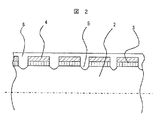
図2において、本発明の骨子を説明する。図2は図1に提示した薄膜抵抗体素子1の部分断面図である。円柱状基体2の表面にはチタン,ニッケル,アルミニウム,タングステン,銅等の導電性部材により下地膜3をスパッタ,蒸着,プラズマ溶射等の薄膜形成方法により形成する。この際下地膜3の膜厚は基体表面の凹凸を覆う程度の膜厚、あるいは少なくとも基体表面、凹凸の1/2以上の膜厚を着膜させる。一旦下地膜3を焼成した後、白金等の感温抵抗体を上層膜4として、下層膜同様な着膜方法により形成し再度焼成する。以降薄膜を形成した基体2両端にリード線6を溶接したキャップ7を挿入した後、抵抗体部分をトリミングにより所定の抵抗値にカットする。最後にオーバーコート8を形成することで薄膜抵抗体素子1は完成する。この際、基体2表面に下地膜を形成した後、熱処理を行わずそのまま上層膜を形成し、下層膜と上層膜を同時に熱処理しても構わない。この場合は同時に下層膜と上層膜が熱処理されることで、下層膜と上層膜として付着した金属原子の集合体が同時に相互拡散することで、基体と下地膜,下地膜と上層膜との間で強固な相互拡散結合が得られるため、着膜信頼性の高い薄膜が得られる。しかしながら、着膜方法がスパッタの場合、複数の金属をスパッタできる装置は設備費用が高くネックである、更に、着膜条件と焼成条件の管理等が格段に厳しくなるため、下層膜を一旦焼成した後、上層膜を形成し焼成する方法が現実的には有利である。
【0018】
以下、図3から図6を用いて再度本発明の特徴を説明する。図3は基体2表面に直接、感温抵抗体膜を形成した抵抗体素子1の部分断面図である。基体2表面の凹凸は通常、5μm程度である。ここに1μmの感温抵抗体膜を形成しても基体2表面の凹凸に沿う形で感温抵抗体膜は形成される。ある部分ではエッチ部9があり、このエッチ部9には薄膜が着膜しにくく、部分的に膜厚が薄くなってしまう。またある部分では薄膜がうねった状態で着膜10され、薄膜としてバランスの悪い状態となる。このような状態での薄膜は前述したように、エッチ部9の薄膜の薄い部分において電気的エネルギー印加状態後の、薄膜の焼損,抵抗値,抵抗温度係数ばらつきの原因となりうる。また均等ではなく、うねった状態での薄膜10形成は薄膜自体の内部歪を生み、信頼性の低い薄膜となってしまう。
【0019】
この問題を解決するため、本発明は考案された。図4は本発明における基体2表面に下地膜3を形成した状態である。基体2表面の凹凸を覆う程度の下地膜3を形成することで、基体2表面の凹凸形状を緩和することが判る。図5は下地膜3の表面に上層膜4を形成した状態である。上層膜4は基体2表面の凹凸を均された下地膜3の上に着膜するため、比較的平坦かつ均等な膜が形成される。図6は所定の抵抗値にトリミングした後の状態である。抵抗体となる上層膜4は平坦な状態のため安定している。図3に示した基体2表面に直接抵抗体薄膜を形成した状態より安定した状態であることは明瞭である。本発明のおける薄膜形成を多層にすることで、均等かつ安定した抵抗体薄膜を得られることで、耐電気特性を向上させることはもちろん、抵抗値、抵抗温度係数ばらつきの少ない品質の優れた抵抗体素子1を得ることができる。
【0020】
図7は本発明の別の実施例である。基体2表面には、基体2表面の凹凸を覆う下地膜3を形成するが、ここでは上層膜4との間に中間膜11が存在する。基体2表面に形成する上層膜4が白金とすると、下地膜3の考慮される部材の線膨張率は以下である。
【0021】
白金:9.0×10⁻⁶/℃
アルミニウム:23.5×10⁻⁶/℃
銅:17.0×10⁻⁶/℃
ニッケル:13.3×10⁻⁶/℃
チタン:8.9×10⁻⁶/℃
タングテン:4.5×10⁻⁶/℃
基本的には下地膜3と上層膜4の線膨張係数は近似していることが望ましく、下地膜3にチタンを用いれば上層膜4の白金と線膨張係数が近似しているため、膜と膜との間に発生する応力は問題とならない。しかしながら、下地膜3に例えばアルミニウムを使用した場合、上層膜4の白金膜との線膨張係数の差分が大きく、過渡的な温度変化が生じた場合、形成した薄膜に応力が発生する。発生応力は線膨張係数の差分に比例して増大するため、下地膜3と上層膜4との界面には応力が発生して、膜間のはがれ、あるいは膜破壊に至ることが懸念される。本発明では、線膨張係数の大きいアルミニウム,銅等を下地膜3にした場合に白金より形成される上層膜4との中間にニッケル等の中間域の線膨張係数を有した部材を中間膜11として形成することで、中間膜11は下地膜3と上層膜4の線膨張係数の差分により生じる応力を緩和する応力緩和部材としての機能持たせることにより、より信頼性の高い薄膜抵抗体素子1を製造できることが可能となる。また逆もしかりである。線膨張係数の小さいタングテンを下地膜3として形成した場合も、上層膜4の白金との間には線膨張係数の差があり、前述したように応力発生が問題となる。この場合、中間膜11にモリブデン等の白金とタングステンの中間付近に位置する線膨張係数の部材で中間膜11を形成し、白金による上層膜4を形成することによっても、上層膜4に発生する応力を緩和する構造の薄膜形成構造となり信頼性の高い薄膜抵抗体素子1となりうる。但し、中間膜11に提示したモリブデンは汎用材料ではないので、中間膜11としてチタンも用いても同様の効果が得られるものである。
【0022】
本発明の別の実施形態として熱式空気流量測定装置用の薄膜抵抗体素子1とした場合の実施例を記載する。発熱抵抗体12及び感温抵抗体13を用いた熱式流量測定装置についての概略について図8を用いて説明する。発熱抵抗体12及び感温抵抗体13を用いた熱式空気流量測定装置の発熱抵抗体12は、空気温度を計測する感温抵抗体13と常に一定の温度差に保たれるように定温度制御回路
14により定温度制御され、常時加熱されている。発熱抵抗体12は空気流の中に設置されるため該空気流に放熱する発熱抵抗体12の表面部分が放熱面、つまり熱伝達面となる。この熱伝達で該空気流に奪われた熱量を電気的信号に変換し空気流量を計測するものである。その全体的な構成は吸入空気を導入しつつ、熱式空気流量測定装置用を保持するボディ15において、全流量の一部が流入する副通路中16に発熱抵抗体12,感温抵抗体13,吸入空気温度測定センサ17が配置されている。これら発熱抵抗体12と感温抵抗体13と定温度制御回路
14はハウジング18に埋設された導電性部材によるターミナル19を介し電気的信号の伝達を行う構造となっている。
【0023】
ここで、本発明による薄膜抵抗体素子1は主に感温抵抗体13として採用することが望ましい。他にも一般産業機器の温度センサー,流量センサー用感温抵抗体素子として活用できうる。
【0024】
【発明の効果】
本発明の目的は基体表面の凹凸を覆う程度の下層膜形成した後に抵抗体となる上層膜を形成することで、耐電気特性に優れた信頼性の高い空気流量測定装置用の抵抗体素子を提供しうる効果がある。
【図面の簡単な説明】
【図1】本発明の特徴を示す抵抗体素子の構造図。
【図2】図1に示した本発明の抵抗体素子の部分断面図。
【図3】市販抵抗器の部分断面図。
【図4】本発明による下層膜形成後の部分断面図。
【図5】本発明による上層膜形成後の部分断面図。
【図6】本発明による抵抗体素子にトリミングを施した後の部分断面図。
【図7】本発明による抵抗体素子の他の実施例。
【図8】本発明の抵抗体素子を熱式空気流量測定装置に組み込んだ実施例。
【符号の説明】
1…薄膜抵抗体素子、2…基体、3…下地膜、4…上層膜、5…切り溝、6…リード線、7…キャップ、8…オーバーコート、9…エッチ部。[0001]
TECHNICAL FIELD OF THE INVENTION
The present invention relates to a resistor element, and more particularly to a resistor element suitably used in a thermal type flow rate measuring device for detecting an air flow rate or a flow velocity in an internal combustion engine by utilizing the temperature dependence of the electrical resistance value of the resistor. It is.
[0002]
[Prior art]
2. Description of the Related Art Conventionally, as a resistor element of this type, a tubular element or a plate element is known. For example, in the element having the former structure, as shown in
[0003]
However, in the case of the former known example, since a thin film serving as a resistor is directly formed on the surface of the substrate, if the surface of the substrate has irregularities, a thin film is formed along the irregularities, and if the irregularities have an etch portion, In the etched portion, the thin film cannot form a predetermined film thickness, and a portion having an extremely thin film is partially formed.
[0004]
Here, when electric surge or electric energy due to radio waves is applied from the outside, the temperature is abnormally increased due to an increase in the current density of the thin edge portion, and in the worst case, the resistor may be burned out. There is. Further, if the thin film formed on the substrate cannot absorb the irregularities on the surface of the substrate, it causes variations in the resistance value and the temperature coefficient of resistance, resulting in defects in quality and reliability.
[0005]
[Patent Document 1]
JP-A-8-75518
[Problems to be solved by the invention]
In view of such circumstances, the present invention has been made, and an object of the present invention is to form a uniform and stable thin film on the substrate surface by absorbing irregularities on the substrate surface. Accordingly, the present invention is intended to improve the electric resistance (generally, anti-electrostatic breakdown) capacity and to provide a temperature-sensitive resistor having a stable variation in resistance value and resistance temperature coefficient.
[0007]
[Means for Solving the Problems]
In order to solve the above problems, according to the present invention, electrical conduction is provided to the ceramic substrate, the resistor provided on the substrate, and the cap capable of electrically conducting the lead electrically conductive. The lower element thin film is formed on the surface of the substrate by a thin film forming method such as sputtering, vapor deposition, or plasma in a resistor element having a structure in which the caps joined by the securing method are inserted into both ends of the substrate. This lower layer thin film is desirably of such a thickness as to be able to fill irregularities on the substrate surface with a transition metal group such as copper, aluminum, nickel and tungsten. After the lower layer thin film is formed, the lower layer film is once baked, and the lower layer thin film is converted into a complete oxide film at a temperature of about 500 ° C. to 1000 ° C. at which the lower layer film is converted into an oxide. Next, the upper layer film is formed on the surface of the lower layer film formed so as to fill the irregularities formed on the substrate surface, and a temperature-sensitive film having a high temperature coefficient of resistance such as Pt is formed by the above-mentioned thin film forming method and baked. The purpose of the present invention is to provide a method for obtaining a desired resistor element.
[0008]
It should be noted that there is no problem even if the lower layer film and the upper layer film formed on the surface of the substrate are fired at the same time. A method in which the lower layer film and the upper layer film, or the lower layer film and the substrate film are simultaneously baked, so that the base film and the lower film film and the lower film film and the upper film are simultaneously bonded to form a stable thin film with reduced residual stress. This also aims to achieve the object of the present invention.
[0009]
BEST MODE FOR CARRYING OUT THE INVENTION
The embodiments of the present invention will be described below to clarify the present invention more specifically, but the present invention is not limited by the description of such examples. Needless to say. In addition, although a film formed on the substrate surface is referred to as a thin film, the thickness is not particularly defined. In general, it is generally said that 1 μm or less is referred to as a thin film, and 1 μm or more is distinguished from a thick film. However, in the present invention, a film formed on a substrate surface without distinction between a thin film and a thick film is indicated. The discussion of the film thickness is out of the scope of the present invention, and the expression "thin film" generally refers to a thin film and a thick film.
[0010]
First, a solid ceramic bobbin having an outer diameter of about 0.5 to 2 mm and a length of about 2 to 4 mm was obtained in order to obtain a thin
[0011]
Further, after forming the
[0012]
After forming a resistive thin film (thickness: about 0.5 μm to 1 μm), a
[0013]
On the other hand, the
[0014]
Here, the
[0015]
As described above, the resistor element used in the air flow measuring device is often installed in an internal combustion engine, and requires considerable consideration for reliability. Of particular concern are ESD (electrostatic damage resistance), surge resistance, and ESD (electromagnetic interference resistance). These are basically electric energy waves, and when these electric energy waves penetrate into electronic components, they promote a local increase in current density in a variation portion of components constituting an electronic circuit, and a local It causes abnormal heating. At worst, it can destroy electronic components. Considering the current environment surrounding vehicles, electrostatic discharge, surge, and EMC due to the above-mentioned discharge are inevitable, and these electric energies always enter the electronic circuit. The electronic circuit is provided with various filters to absorb the electric energy that enters from the outside, but it is still difficult to completely shield the electronic circuit from the external electric energy. It is in a state. Furthermore, in the heating resistor type air flow measuring device which measures the air flow by exposing the
[0016]
In the present invention, a thin
[0017]
FIG. 2 illustrates the gist of the present invention. FIG. 2 is a partial sectional view of the thin-
[0018]
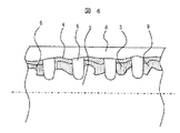
Hereinafter, the features of the present invention will be described again with reference to FIGS. FIG. 3 is a partial sectional view of the
[0019]
To solve this problem, the present invention has been devised. FIG. 4 shows a state in which a
[0020]
FIG. 7 shows another embodiment of the present invention. A
[0021]
Platinum: 9.0 × 10 −6 / ° C
Aluminum: 23.5 × 10 −6 / ° C
Copper: 17.0 × 10 −6 / ° C.
Nickel: 13.3 × 10 −6 / ° C
Titanium: 8.9 × 10 −6 / ° C.
Tang ten: 4.5 × 10 −6 / ° C.
Basically, it is desirable that the linear expansion coefficients of the
[0022]
As another embodiment of the present invention, an example in which the thin
[0023]
Here, it is desirable that the thin-
[0024]
【The invention's effect】
An object of the present invention is to form a resistive element for a highly reliable air flow measuring device having excellent electric resistance characteristics by forming a resistive element having an electric resistance characteristic by forming a resistive element after forming a resistive element so as to cover irregularities on a substrate surface. There are effects that can be provided.
[Brief description of the drawings]
FIG. 1 is a structural view of a resistor element showing features of the present invention.
FIG. 2 is a partial cross-sectional view of the resistor element of the present invention shown in FIG.
FIG. 3 is a partial sectional view of a commercially available resistor.
FIG. 4 is a partial cross-sectional view after forming a lower layer film according to the present invention.
FIG. 5 is a partial cross-sectional view after forming an upper layer film according to the present invention.
FIG. 6 is a partial cross-sectional view after trimming is performed on the resistor element according to the present invention.
FIG. 7 shows another embodiment of the resistor element according to the present invention.
FIG. 8 shows an embodiment in which the resistor element of the present invention is incorporated in a thermal air flow measuring device.
[Explanation of symbols]
DESCRIPTION OF
Claims (9)
該基体表面に、前記基体表面の凹凸を覆う薄膜層を下層膜として形成した後、上層薄膜として感温抵抗体を形成することを特徴とした抵抗体素子。A ceramic base and a resistor provided on the base and adjusted to a predetermined resistance value are connected to a lead formed of a conductive metal member on a cap shaped to be fitted with the base. A resistor element having a cap made of a member, wherein the cap is fitted and fixed to both ends of the base, and a protective film is coated on the entire circumference of the base on which the resistor is formed,
A resistor element comprising: forming a thin film layer covering the irregularities on the surface of the substrate as a lower layer film on the surface of the substrate, and then forming a temperature-sensitive resistor as an upper layer thin film.
該基体表面に形成する下層膜と、その表面に形成する上層膜との中間に更にもう一層の中間膜を形成したことを特徴とする抵抗体素子。A ceramic base and a resistor provided on the base and adjusted to a predetermined resistance value are connected to a lead formed of a conductive metal member on a cap shaped to be fitted with the base. A resistor element having a cap made of a member, wherein the cap is fitted and fixed to both ends of the base, and a protective film is coated on the entire circumference of the base on which the resistor is formed,
A resistor element comprising a further intermediate film formed between a lower film formed on the surface of the substrate and an upper film formed on the surface.
Priority Applications (1)
| Application Number | Priority Date | Filing Date | Title |
|---|---|---|---|
| JP2003158786A JP2004363264A (en) | 2003-06-04 | 2003-06-04 | Resistor element |
Applications Claiming Priority (1)
| Application Number | Priority Date | Filing Date | Title |
|---|---|---|---|
| JP2003158786A JP2004363264A (en) | 2003-06-04 | 2003-06-04 | Resistor element |
Publications (1)
| Publication Number | Publication Date |
|---|---|
| JP2004363264A true JP2004363264A (en) | 2004-12-24 |
Family
ID=34052025
Family Applications (1)
| Application Number | Title | Priority Date | Filing Date |
|---|---|---|---|
| JP2003158786A Pending JP2004363264A (en) | 2003-06-04 | 2003-06-04 | Resistor element |
Country Status (1)
| Country | Link |
|---|---|
| JP (1) | JP2004363264A (en) |
Cited By (2)
| Publication number | Priority date | Publication date | Assignee | Title |
|---|---|---|---|---|
| JP2006283285A (en) * | 2005-03-31 | 2006-10-19 | Kajima Corp | Tunnel joining method |
| JP2017516081A (en) * | 2014-03-26 | 2017-06-15 | ヘレウス センサー テクノロジー ゲーエムベーハー | Ceramic carrier, sensor element having ceramic carrier, heating element and sensor module, and method for producing ceramic carrier |
-
2003
- 2003-06-04 JP JP2003158786A patent/JP2004363264A/en active Pending
Cited By (4)
| Publication number | Priority date | Publication date | Assignee | Title |
|---|---|---|---|---|
| JP2006283285A (en) * | 2005-03-31 | 2006-10-19 | Kajima Corp | Tunnel joining method |
| JP4627209B2 (en) * | 2005-03-31 | 2011-02-09 | 鹿島建設株式会社 | Tunnel joining method |
| JP2017516081A (en) * | 2014-03-26 | 2017-06-15 | ヘレウス センサー テクノロジー ゲーエムベーハー | Ceramic carrier, sensor element having ceramic carrier, heating element and sensor module, and method for producing ceramic carrier |
| US10529470B2 (en) | 2014-03-26 | 2020-01-07 | Heraeus Nexensos Gmbh | Ceramic carrier and sensor element, heating element and sensor module, each with a ceramic carrier and method for manufacturing a ceramic carrier |
Similar Documents
| Publication | Publication Date | Title |
|---|---|---|
| US11382182B2 (en) | Planar heating element with a PTC resistive structure | |
| RU2284595C2 (en) | STABLE TUNGSTEN-ON-AlN HIGH-TEMPERATURE SENSOR/HEATER SYSTEM AND METHOD THEREOF | |
| US5823680A (en) | Temperature sensor | |
| JP5623015B2 (en) | Self-cleaning action of flow sensor element and flow sensor element | |
| US7721599B2 (en) | Reduced resistance thermal flow measurement device | |
| JP6988585B2 (en) | Sensor element and gas sensor equipped with it | |
| US5652443A (en) | Sensor having a micro-bridge heater | |
| JP2004363264A (en) | Resistor element | |
| WO2020244682A1 (en) | Heating element and atomization device | |
| US7880580B2 (en) | Thermistor having doped and undoped layers of material | |
| JPS62263417A (en) | Thermal flow rate sensor | |
| JPS62265529A (en) | Device for measuring flow rate of medium and manufacture thereof | |
| JPH11354302A (en) | Thin-film resistor element | |
| JP3452282B2 (en) | Composite thermistor temperature sensor | |
| JPH08138906A (en) | Manufacture of positive temperature coefficient(ptc) thermistor device and heat detecting device | |
| JPH0632267B2 (en) | Electric heater | |
| KR101848764B1 (en) | Micro temperature sensor and fabrication method of the same | |
| JP7042087B2 (en) | Temperature sensor | |
| JP2003059704A (en) | Temperature sensitive resistor device and thermal flow sensor | |
| JP2000111379A (en) | Flow-rate detecting device and its manufacture | |
| JP2021012049A (en) | Temperature sensor element | |
| JPH102774A (en) | Heating element | |
| JP3701184B2 (en) | Thermal flow measuring device and resistor element used therefor | |
| JP2017215287A (en) | Temperature sensor | |
| JPH10274552A (en) | Thermal type flow velocity sensor |
Legal Events
| Date | Code | Title | Description |
|---|---|---|---|
| A621 | Written request for application examination |
Free format text: JAPANESE INTERMEDIATE CODE: A621 Effective date: 20051201 |
|
| RD01 | Notification of change of attorney |
Free format text: JAPANESE INTERMEDIATE CODE: A7421 Effective date: 20060420 |
|
| A131 | Notification of reasons for refusal |
Free format text: JAPANESE INTERMEDIATE CODE: A131 Effective date: 20080826 |
|
| A02 | Decision of refusal |
Free format text: JAPANESE INTERMEDIATE CODE: A02 Effective date: 20090310 |