JP2004363256A - Semiconductor device and method of manufacturing semiconductor device - Google Patents
Semiconductor device and method of manufacturing semiconductor device Download PDFInfo
- Publication number
- JP2004363256A JP2004363256A JP2003158487A JP2003158487A JP2004363256A JP 2004363256 A JP2004363256 A JP 2004363256A JP 2003158487 A JP2003158487 A JP 2003158487A JP 2003158487 A JP2003158487 A JP 2003158487A JP 2004363256 A JP2004363256 A JP 2004363256A
- Authority
- JP
- Japan
- Prior art keywords
- wiring
- semiconductor device
- insulating film
- via plugs
- wirings
- Prior art date
- Legal status (The legal status is an assumption and is not a legal conclusion. Google has not performed a legal analysis and makes no representation as to the accuracy of the status listed.)
- Withdrawn
Links
Images
Classifications
-
- H—ELECTRICITY
- H10—SEMICONDUCTOR DEVICES; ELECTRIC SOLID-STATE DEVICES NOT OTHERWISE PROVIDED FOR
- H10W—GENERIC PACKAGES, INTERCONNECTIONS, CONNECTORS OR OTHER CONSTRUCTIONAL DETAILS OF DEVICES COVERED BY CLASS H10
- H10W20/00—Interconnections in chips, wafers or substrates
- H10W20/01—Manufacture or treatment
- H10W20/071—Manufacture or treatment of dielectric parts thereof
- H10W20/081—Manufacture or treatment of dielectric parts thereof by forming openings in the dielectric parts
- H10W20/084—Manufacture or treatment of dielectric parts thereof by forming openings in the dielectric parts for dual-damascene structures
- H10W20/085—Manufacture or treatment of dielectric parts thereof by forming openings in the dielectric parts for dual-damascene structures involving intermediate temporary filling with material
-
- H—ELECTRICITY
- H10—SEMICONDUCTOR DEVICES; ELECTRIC SOLID-STATE DEVICES NOT OTHERWISE PROVIDED FOR
- H10W—GENERIC PACKAGES, INTERCONNECTIONS, CONNECTORS OR OTHER CONSTRUCTIONAL DETAILS OF DEVICES COVERED BY CLASS H10
- H10W20/00—Interconnections in chips, wafers or substrates
- H10W20/01—Manufacture or treatment
- H10W20/031—Manufacture or treatment of conductive parts of the interconnections
-
- H—ELECTRICITY
- H10—SEMICONDUCTOR DEVICES; ELECTRIC SOLID-STATE DEVICES NOT OTHERWISE PROVIDED FOR
- H10W—GENERIC PACKAGES, INTERCONNECTIONS, CONNECTORS OR OTHER CONSTRUCTIONAL DETAILS OF DEVICES COVERED BY CLASS H10
- H10W20/00—Interconnections in chips, wafers or substrates
- H10W20/01—Manufacture or treatment
- H10W20/071—Manufacture or treatment of dielectric parts thereof
- H10W20/081—Manufacture or treatment of dielectric parts thereof by forming openings in the dielectric parts
- H10W20/084—Manufacture or treatment of dielectric parts thereof by forming openings in the dielectric parts for dual-damascene structures
-
- H—ELECTRICITY
- H10—SEMICONDUCTOR DEVICES; ELECTRIC SOLID-STATE DEVICES NOT OTHERWISE PROVIDED FOR
- H10W—GENERIC PACKAGES, INTERCONNECTIONS, CONNECTORS OR OTHER CONSTRUCTIONAL DETAILS OF DEVICES COVERED BY CLASS H10
- H10W20/00—Interconnections in chips, wafers or substrates
- H10W20/40—Interconnections external to wafers or substrates, e.g. back-end-of-line [BEOL] metallisations or vias connecting to gate electrodes
- H10W20/41—Interconnections external to wafers or substrates, e.g. back-end-of-line [BEOL] metallisations or vias connecting to gate electrodes characterised by their conductive parts
- H10W20/427—Power or ground buses
-
- H—ELECTRICITY
- H10—SEMICONDUCTOR DEVICES; ELECTRIC SOLID-STATE DEVICES NOT OTHERWISE PROVIDED FOR
- H10W—GENERIC PACKAGES, INTERCONNECTIONS, CONNECTORS OR OTHER CONSTRUCTIONAL DETAILS OF DEVICES COVERED BY CLASS H10
- H10W20/00—Interconnections in chips, wafers or substrates
- H10W20/40—Interconnections external to wafers or substrates, e.g. back-end-of-line [BEOL] metallisations or vias connecting to gate electrodes
- H10W20/41—Interconnections external to wafers or substrates, e.g. back-end-of-line [BEOL] metallisations or vias connecting to gate electrodes characterised by their conductive parts
- H10W20/435—Cross-sectional shapes or dispositions of interconnections
Landscapes
- Internal Circuitry In Semiconductor Integrated Circuit Devices (AREA)
Abstract
【課題】半導体装置のローカル配線層部での配線間容量を抑え、配線の信頼性を向上する。
【解決手段】半導体基板40上に形成された第1配線層部33と、第1配線層部33上に形成された第2配線層部32とを具備する半導体装置を用いる。第1配線層部33は、第1層間絶縁膜と、第1層間絶縁膜内に第1間隔以上で設けられた複数の第1ビアプラグ37−1及び複数の第1配線37−2とを有する。第2配線層部32は、第2層間絶縁膜と、第2層間絶縁膜内に第1間隔よりも大きい第2間隔以上で設けられた複数の第2ビアプラグ34−1及び複数の第2配線34−2とを有する。第1ビアプラグ37−1、第1配線37−2、第2ビアプラグ34−1及び第2配線34−2は、銅を含む金属からなる。第1配線層部33は、シングルダマシン構造であり、第2配線層部32は、デュアルダマシン構造である。
【選択図】 図1An object of the present invention is to reduce the capacitance between wirings in a local wiring layer portion of a semiconductor device and improve the reliability of wiring.
A semiconductor device includes a first wiring layer portion formed on a semiconductor substrate and a second wiring layer portion formed on the first wiring layer portion. The first wiring layer portion 33 has a first interlayer insulating film, a plurality of first via plugs 37-1 and a plurality of first wirings 37-2 provided in the first interlayer insulating film at first intervals or more. . The second wiring layer part 32 includes a second interlayer insulating film, a plurality of second via plugs 34-1 and a plurality of second wirings provided in the second interlayer insulating film at a second interval or more that is greater than the first interval. 34-2. The first via plug 37-1, the first wiring 37-2, the second via plug 34-1 and the second wiring 34-2 are made of a metal containing copper. The first wiring layer portion 33 has a single damascene structure, and the second wiring layer portion 32 has a dual damascene structure.
[Selection diagram] Fig. 1
Description
【0001】
【発明の属する技術分野】
本発明は、半導体装置及び半導体装置の製造方法に関し、特に、銅を含む金属からなるダマシン構造の配線及びビアプラグを備える半導体装置及び半導体装置の製造方法に関する。
【0002】
【従来の技術】
半導体装置の配線に関わる構造として、半導体基板上に設けられた複数の素子上に、ローカル配線層部と電源配線層部とが順に積層された構造が知られている。そのような半導体装置では、各層における配線には材料として銅(Cu)を用い、各層間の接続に用いられるビアプラグには材料としてタングステン(W)を用いるのが一般的である。
【0003】
しかし、タングステンの成膜温度は非常に高いため、微細化された配線の銅が耐え切れず、凝集が起こり、断線する確率が高くなる。一方、銅を用いたビアプラグは、タングステンを用いたビアプラグに比較して、ビア抵抗が低い、熱応力に対する耐性が高いなどの利点がある。このような理由から、近年、ビアプラグにも銅を用いることが多くなってきている。
【0004】
配線及びビアプラグを共に銅で形成する方法として、デュアルダマシン法及びシングルダマシン法がある。デュアルダマシン法は、シングルダマシン法に比較して、CMPの工程が1回少ない、配線とビアプラグとの間にバリアメタル膜が挟まっていないので配線抵抗が小さい、という点で利点がある。そのため、現在、配線及びビアプラグを全てデュアルダマシン法で形成することが多い。そのような半導体装置の構造について図7を参照して説明する。
【0005】
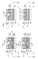
図7は、半導体装置の配線に関わる構造を示す断面図である。半導体装置101は、半導体基板140上に設けられ、素子部131、ローカル配線層部133及び電源配線層部132を具備する。素子部131は、半導体基板140及びその上に設けられた複数の素子及びその配線(図示されず)を備える。
【0006】
ローカル配線層部133は、素子部131上に設けられ、複数の配線137−2と複数のビアプラグ137−1とを含む配線層133−1を備える。配線137−2は、複数の素子に対して信号の入出力を行う信号線、又は、複数の素子と電源配線層部132とを接続する電源線又は接地線である。ビアプラグ137−1は、配線137−2同士、又は、配線137−2と素子との間を接続する。
そして、配線137−2とビアプラグ137−1とで形成される接合部138は、デュアルダマシン法で形成されている。
【0007】
電源配線層部132は、ローカル配線層部133の上に設けられ、複数の配線134−2と複数のビアプラグ134−1とを含む配線層132−1を備える。ローカル配線層部133と接続するビアプラグ134−1を特にビアプラグ136ともいう。配線134−2は、複数の素子に対して電源を接続する電源線、又は、接地を行う接地線である。ビアプラグ134−1は、配線134−2同士を接続する。そして、配線134−2とビアプラグ134−1とで形成される接合部135は、デュアルダマシン法で形成されている。
【0008】
ここで、デュアルダマシン法には、ビアファースト法とトレンチファースト法とがある。ビアファースト法は、露光時の反射防止のために、ビアホールの開口後、配線溝(トレンチ)を形成する前に、ビアホールをBARC(BottomAnti−Reflection Coating、)で埋める必要がある。そのため、工程が煩雑になる。従って、工程の少ないトレンチファースト法が好んで用いられる。
【0009】
しかし、トレンチファースト法では、ビアホールをフォトリソグラフィーの技術で形成する際、配線溝(トレンチ)の段差を有する半導体装置上にレジストを塗布し、所定のパターンを露光する必要がある。そのため、配線溝のパターンによっては、段差により焦点を適切に合わすことが困難となる。特に、微細な形状を正確に露光できなくなる。従って、ローカル配線層部133のようなビアプラグの大きさが小さく、かつ、そのピッチが狭いところでは、ビアファースト法でビアホールを形成することが一般的となっている。
【0010】
以下、デュアルダマシン法の一つであるビアファースト法について説明する。図8〜図11は、ビアファースト法のプロセスを示す半導体装置の断面図である。ここでは、2つの層のそれぞれに設けられた配線と、それらを繋ぐビアプラグとを形成する例を示す。
【0011】
図8(a)に示すように、基板140上において、層間絶縁膜103上のストッパ絶縁層104及び低誘電率絶縁層105の中に、第1層の配線110が設けられる。配線110は、銅(Cu)の配線109とタンタル/窒化タンタル(Ta/TaN)のバリアメタル層108を含み、ダマシン構造を有する。従来知られた配線製造プロセスで設けられる。そして、配線110と低誘電率絶縁層105とを覆うようにストッパ絶縁膜114aが設けられる。更に、ストッパ絶縁膜114aを覆うように層間絶縁膜115aが設けられる。更に、層間絶縁膜115aを覆うようにストッパ絶縁膜124aが設けられる。更に、ストッパ絶縁膜124aを覆うように低誘電率絶縁膜125aが設けられる。
【0012】
続いて、図8(a)の状態から、フォトリソグラフィーのプロセスを用いて、層間絶縁膜115a、ストッパ絶縁膜124a及び低誘電率絶縁膜125aに、ビアホール107を形成する。この状態が図8(b)である。このとき、ビアホール107を形成された層間絶縁膜115a、ストッパ絶縁膜124a及び低誘電率絶縁膜125aを、それぞれ、層間絶縁層115、ストッパ絶縁層124b及び低誘電率絶縁層125bとする。
【0013】
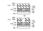
次に、図8(b)の状態から、ビアホール107に有機物142(例示:BARC)を埋め込む。有機物142の量(ビアホール107での有機物142の高さhA)は、ビアホール107の密度やその他の要因で決まる。ここでは、ストッパ絶縁層124bの高さまでとする。この状態が図9(a)及び(c)である。ただし、図9(c)は、図9(a)でのAA’断面である。このときのビアホール107をビアホール107aとする。
【0014】
続いて、図9(a)及び(c)の状態から、フォトリソグラフィーのプロセスを用いて、低誘電率絶縁層125bに、配線溝117aを形成する。この状態が図9(b)及び(d)である。ただし、図9(d)は、図9(b)でのBB’断面である。このとき、低誘電率絶縁層125b及びビアホール107aを、それぞれ、低誘電率絶縁層125及びビアホール107bとする。
【0015】
次に、図9(b)及び(d)の状態から、有機物142を除去する。そして、ビアホール107bの底部のストッパ絶縁膜114aと、配線溝117の底部のストッパ絶縁膜124bとをエッチバックして除去する。この状態が図10(a)及び(c)である。ただし、図10(c)は、図10(a)でのCC’断面である。このとき、ビアホール107b、配線溝117a、ストッパ絶縁膜114a及びストッパ絶縁膜124aを、それぞれビアホール107c、配線溝117、ストッパ絶縁層114及びストッパ絶縁層124とする。
【0016】
続いて、図10(a)及び(c)の状態から、低誘電率絶縁層125の表面と、配線溝117の側壁(側面)及び底部と、ビアホール107cの側壁(側面)及び底部とを覆うように、Ta/TaNからなるバリアメタル膜118aをスパッタ法で設ける。次に、バリアメタル膜118aを覆うようにCuからなるシード導体膜119aを設ける。続いて、シード導体膜119aを覆い、且つ、配線溝117b及びビアホール107eを埋めるようにCuからなる導体膜119bを設ける。この状態が図10(b)及び(d)である。ただし、図10(d)は、図10(b)でのDD’断面である。
【0017】
次に、図10(b)及び(d)の状態から、低誘電率絶縁層125表面及び配線溝117上方における不要なバリアメタル膜118a、シード導体膜119a及び導体膜119bをCMP(Chemical Mechanical Polishing)で除去する。このようにして、元々のビアホール107においてバリアメタル層118及び導体層119とからなるビアプラグ120(コンタクト)が形成される。また、元々の配線溝117においてバリアメタル層118及び導体層119とからなる配線130が形成される。この状態が図11(a)及び(b)である。ただし、図11(b)は、図11(a)でのEE’断面である。
【0018】
このように図8〜図11の製造方法により、デュアルダマシン法の一つであるビアファースト法により配線及びビアプラグが形成される。ただし、図11におけるビアプラグ120、配線130及び配線110は、それぞれ図7におけるビアプラグ137−1、配線137−2に対応する。
【0019】
電源配線層部132に用いるデュアルダマシン法の一つであるトレンチファースト法は、ビアファースト法とは逆に、まず、配線溝117を形成する。そして、配線溝117の底部の所定の位置に、フォトリソグラフィーの技術によりビアホール107を形成する。その後のプロセス(バリアメタル層118及び導体層119の形成等)は、ビアファースト法と同様である。
【0020】
関連する技術として、特開2001−156168号公報(特許文献1)に、半導体装置とその製造方法の技術が開示されている。この技術の半導体装置は、半導体基板と、複数の配線層とを有する。半導体基板は、複数の素子が形成されている。複数の配線層は、前記半導体基板上に形成されている。複数の配線層は、前記複数の素子同士を接続するための銅からなる信号線や前記複数の素子に電源を供給するための銅からなる電源線及び接地線を備える。そして、前記複数の配線層間における信号線、電源線及び接地線の接続が、前記信号線、電源線及び接地線下に形成されたビアによってなされる。ここで、前記信号線及び前記信号線下に形成された第1ビアは、該ビアにタングステンを用いてシングルダマシン工程によって形成されている。前記電源線及び接地線、並びに該電源線及び接地線下に形成された第2ビアは、デュアルダマシン工程によって形成されている。第2ビアの面積は、第1ビアの面積よりも予め設定された割合だけ大きくなるように形成されている。
この技術は、機械的強度が強く、かつ、放熱性に優れた半導体装置及びその製造方法を提供することを目的とする。
【0021】
【特許文献1】
特開2001−156168号公報(図1(b)、図6、図7、図8)
【0022】
【発明が解決しようとする課題】
図9(b)及び(d)において、有機物142の最上部の位置は、ビアホール107内のストッパ絶縁層124bの位置と同じになっている。実際の半導体装置では、同一層に複数のビアホール107が存在し、ビアホール107が密集した領域(密領域)とそうでない領域(疎領域)とがある。同一層上には、表面の単位面積あたり、一定の有機物142が供給される。そのため、密領域において有機物142の最上部の位置とストッパ絶縁層124bの位置とが同じになるように、BARCを供給すると、疎領域において有機物142の最上部の位置がストッパ絶縁膜124bの位置より高くなる。反対に、疎領域において有機物142の最上部の位置とストッパ絶縁層124bの位置とが同じになるように、BARCを供給すると、密領域において有機物142の最上部の位置がストッパ絶縁膜124bの位置より低くなる。
【0023】
ビアホール107において、有機物142の最上部の位置がストッパ絶縁膜124bの位置より高くなると、以下のような問題が生じる。
【0024】
図12は、有機物の最上部の位置がストッパ絶縁膜の位置より高くなるように有機物を入れた場合の半導体装置の断面を示す図である。図12(a)は、図9(a)に対応する。図12(c)は、図12(a)のFF’断面である。有機物142’は、低誘電率層125bの高さまで埋め込まれている。この状態から、フォトリソグラフィーのプロセスを用いて、低誘電率絶縁層125bに、配線溝117aを形成する。この状態が図12(b)及び(d)である。ただし、図12(d)は、図12(b)でのGG’断面である。この場合、配線溝117aをエッチングで形成する際、エッチング残渣が、配線溝117内に出た有機物142’の側面に付着して、フェンス(膜)145を形成する。フェンス145は、有機物142’を除去した後も残る。そのため、フェンス145は、その後のバリアメタル膜118aやシード導体膜119aを形成する障害となる。そして、配線の抵抗の増大や断線のような問題が発生し、信頼性を低下させる原因となる。
【0025】
一方、ビアホール107において、有機物142の最上部の位置がストッパ絶縁膜124bの位置より低くなると、以下のような問題が生じる。
【0026】
図13は、有機物の最上部の位置がストッパ絶縁膜の位置より低くなるように有機物を入れた場合の半導体装置の断面図である。図13(a)は、図9(a)に対応する。図13(c)は、図13(a)のHH’断面である。このときのビアホール107をビアホール107a’とする。この状態から、フォトリソグラフィーのプロセスを用いて、低誘電率絶縁層125bに、配線溝117を形成する。この状態が図13(b)及び(d)である。ただし、図13(d)は、図13(b)でのII’断面である。このとき、ストッパ絶縁層124b、低誘電率絶縁層125b及びビアホール107a’を、それぞれ、ストッパ絶縁層124’、低誘電率絶縁層125’及びビアホール107b’とする。このとき、ストッパ絶縁層124’及び層間絶縁膜115は、ビアホール107b’との境界部分において、一部分がエッチングされてしまう。それにより、ストッパ絶縁層124’の除去された肩落ち部146が形成される。図13(d)に示すように、特に配線溝117’の方向にそれが顕著に現れる。その理由は、角の部分(この場合、ビアホール107b’の開口部)ができると、その部分のエッチング速度が、他の部分のエッチング速度と比較して速くなるからである。
【0027】
その後、図13(b)及び(d)の状態から、有機物142’’を除去する。その後、ビアホール107b’の底部のストッパ絶縁膜114aと、配線溝117’の底部のストッパ絶縁膜124とをエッチバックして除去する。続いて、バリアメタル膜118a、シード導体膜119a、導体膜119bを設ける。そして、低誘電率絶縁層125表面及び配線溝117’上方における不要なバリアメタル膜118a、シード導体膜119a及び導体膜119bをCMPで除去し、ビアプラグ120及び配線130が形成される。この状態が図14(a)及び(b)である。ただし、図14(b)は、図14(a)でのJJ’断面である。このとき、肩落ち部146の配線130は、配線の長さ方向の断面積を増加させることになる。すなわち、配線間容量の増加の原因となる。
【0028】
近年の半導体装置の微細化の進展において、配線の信頼性を維持することは重要である。具体的には、バリアメタル膜を厚く成膜して銅のマイグレーションや絶縁膜への拡散を防止すること、図12で説明した理由からビアホールに埋め込む有機物を多くせずキャップ絶縁層の高さより低くすること、などが必要である。その場合、バリアメタル膜が厚いことによる配線の抵抗の増加、図13及び図14で説明した肩落ち部146aの形成、などが起きる。
【0029】
図15は、図13及び図14の肩落ちを含む半導体装置の配線に関わる構造を示す断面図である。半導体装置101aは、素子部131a、ローカル配線層部133a及び電源配線層部132aを具備する。素子部131a、ローカル配線層部133a及び電源配線層部132aは、基本的に図7の素子部131、ローカル配線層部133及び電源配線層部132と同様である。ただし、ローカル配線層部133aは、ビアプラグ137a−1のピッチが狭くなっている。また、図13及び図14で説明したように、肩落ち部146a(−1〜2)が形成されることになる。ただし、肩落ち部146a−2は、肩落ち部146a−1と向きが90度異なり、紙面に垂直な方向において、図14(b)のような肩落ちが生じている。
【0030】
この場合、ビアプラグ137a−1のピッチが小さくなり、個々の肩落ち部146a同士の距離は近くなっている。加えて、肩落ち部146aにより、配線の長さ方向の断面積が増加している。それらのことから、ビアプラグ周辺での肩落ち部146aの形成による配線間容量の増加は無視できない問題となる。
【0031】
半導体装置におけるローカル配線層部での配線やビアプラグの信頼性を向上する技術が望まれている。配線間容量の増加を防止する技術が求められている。配線の抵抗の増加を防止する技術が望まれている。電源配線層部でのビアプラグの抵抗を低く保ち、その工程数を削減することが可能な技術が求められている。
【0032】
従って、本発明の目的は、ローカル配線層部での配線やビアプラグの信頼性を向上する半導体装置及び半導体装置の製造方法を提供することである。
【0033】
また、本発明の別の目的は、ローカル配線層部で配線間容量及び配線抵抗の増加を防止する半導体装置及び半導体装置の製造方法を提供することである。
【0034】
本発明の更に別の目的は、動作の信頼性を向上することが可能な半導体装置及び半導体装置の製造方法を提供することである。
【0035】
本発明の他の目的は、電源配線層部でのビアプラグの抵抗を低く保ち、その工程数を削減することが可能な半導体装置及び半導体装置の製造方法を提供することである。
【0036】
【課題を解決するための手段】
以下に、[発明の実施の形態]で使用される番号・符号を用いて、課題を解決するための手段を説明する。これらの番号・符号は、[特許請求の範囲]の記載と[発明の実施の形態]との対応関係を明らかにするために付加されたものである。ただし、それらの番号・符号を、[特許請求の範囲]に記載されている発明の技術的範囲の解釈に用いてはならない。
【0037】
従って、上記課題を解決するために、本発明の半導体装置は、半導体基板(40)上に形成された第1配線層部(33)と、第1配線層部(33)上に形成された第2配線層部(32)とを具備する。第1配線層部(33)は、第1層間絶縁膜と、複数の第1ビアプラグ(37−1)と、複数の第1配線(37−2)を有する。複数の第1ビアプラグ(37−1)は、その第1層間絶縁膜内に設けられ第1間隔以上で互いに隔てられている。複数の第1配線(37−2)は、その第1層間絶縁膜内において複数の第1ビアプラグ(37−1)上に設けられ複数の第1ビアプラグ(37−1)に接続されている。第2配線層部(32)は、第2層間絶縁膜と、複数の第2ビアプラグ(34−1)と、複数の第2配線(34−2)を有する。複数の第2ビアプラグ(34−1)は、その第2層間絶縁膜内に設けられその第1間隔よりも大きい第2間隔以上で互いに隔てられている。複数の第2配線(34−2)は、その第2層間絶縁膜内において複数の第2ビアプラグ(34−1)上に設けられ複数の第2ビアプラグ(34−1)に接続されている。複数の第1ビアプラグ(37−1)、複数の第1配線(37−2)、複数の第2ビアプラグ(34−1)及び複数の第2配線(34−2)は、銅を含む金属からなる。第1配線層部(33)は、シングルダマシン構造であり、第2配線層部(32)は、デュアルダマシン構造である。
【0038】
本発明により、半導体装置の第2配線層部(32)よりもビアプラグの間隔が狭い第1配線層部(33)において、シングルダマシン構造を採用することにより、図14に示す肩落ち部(146)の生成を防止することができる。それにより、デュアルダマシン構造の場合に比較して、配線間容量を抑えることが可能となる。
【0039】
上記の半導体装置において、第1配線層部(33)は、その第1層間絶縁膜内に設けられた複数の第1ビアプラグ(37−1)と複数の第1配線(37−2)とを含む複数の層を備える。第2配線層部(32)は、その第2層間絶縁膜内に設けられた複数の第2ビアプラグ(34−1)と複数の第2配線(34−2)とを含む複数の層を備える。
【0040】
上記の半導体装置において、その第1間隔は、複数の第1ビアプラグ(37−1)に関する単位面積あたりのビアプラグの個数としてのビア密度(n)が、所定の条件を満たすように設定される。その所定の条件は、複数の第1配線(37−2)の各々間の配線間容量(CS)が、第1配線層部(33)をデュアルダマシン法で形成した場合(CD)に比較して、小さくなることである。
【0041】
ビア密度(n)が大きくなるとデュアルダマシン法による肩落ち部(146)の影響が大きくなるが、本発明ではそのような影響の出る状況(所定の条件)において、シングルダマシン法で作成しているので、配線間容量の増加を防止することができる。
【0042】
上記の半導体装置において、ビア密度(n)は、1個/μm2以上である。
肩落ち部(146)の影響がでるのは、特に、ビア密度(n)が1個/μm2以上においてであり、本発明をその範囲に適用することで、配線間容量の増加を防止することができる。
【0043】
上記の半導体装置において、その第1間隔は、0.5μmである。
本発明をその範囲に適用することで、配線間容量の増加を防止することができる。
【0044】
上記の半導体装置において、複数の第1ビアプラグ(37−1)の各々の直径は、0.4μm以下である。
第1ビアプラグ(37−1)の各々の直径が0.4μm以下の場合、特に、ビアファースト法を用いるので、本発明をその範囲に適用することで、配線間容量の増加を防止することができる。
【0045】
また、上記課題を解決するために、本発明の半導体装置の製造方法は、(a)〜(f)工程を備える。(a)は、半導体基板(40)上に第1絶縁膜を形成する工程である。(b)は、その第1絶縁膜に第1間隔以上で互いに隔てられた銅を含む金属からなる複数の第1ビアプラグ(37−1)をシングルダマシン法により形成する工程である。(c)は、その第1絶縁膜及び複数の第1ビアプラグ(37−1)上に第2絶縁膜を形成する工程である。(d)は、その第2絶縁膜に複数の第1ビアプラグ(37−1)に接続された銅を含む金属からな複数の第1配線(37−2)をシングルダマシン法により形成する工程である。(e)は、その第2絶縁膜及び複数の第1配線(37−2)上に第3絶縁膜を形成する工程である。(f)は、その第3絶縁膜にその第1間隔よりも大きい第2間隔以上で互いに隔てられた複数の第2ビアプラグ(34−1)及び複数の第2ビアプラグ(34−1)に接続された銅を含む金属からなる複数の第2配線(34−2)をデュアルダマシン法により形成する工程である。
【0046】
上記の半導体装置の製造方法において、そのデュアルダマシン法は、トレンチファースト法である。
【0047】
上記の半導体装置の製造方法において、(g)〜(h)工程を更に備える。(g)は、(d)工程と(e)工程との間で、(a)工程から(d)工程を、所望の層数分繰り返す工程である。(h)は、(f)工程の後で、(e)工程から(f)工程を、所望の層数分繰り返す工程である。
【0048】
上記の半導体装置の製造方法において、その第1間隔は、複数の第1ビアプラグ(37−1)に関する単位面積あたりのビアプラグの個数としてのビア密度(n)が、所定の条件を満たすように設定される。その所定の条件は、複数の第1配線(37−2)の各々間の配線間容量(CS)が、複数の第1ビアプラグ(37−1)及び複数の第1配線(37−2)をデュアルダマシン法で形成した場合(CD)に比較して、小さくなることである。
【0049】
上記の半導体装置の製造方法において、ビア密度(n)は、1個/μm2以上である。
【0050】
上記の半導体装置の製造方法において、その第1間隔は、0.5μmである。
【0051】
上記の半導体装置の製造方法において、複数の第1ビアプラグ(37−1)の各々の直径は、0.4μm以下である。
【0052】
【発明の実施の形態】
以下、本発明の半導体装置及び半導体装置の製造方法の実施の形態に関して、添付図面を参照して説明する。
【0053】
まず、本発明の半導体装置の実施の形態の構成について説明する。
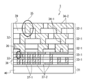
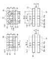
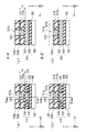
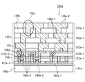
図1は、本発明の半導体装置の配線に関わる構造を示す断面図である。半導体装置1は、素子部31、ローカル配線層部33及び電源配線層部32を具備する。
【0054】
素子部31は、半導体基板40及びその上に設けられた複数の素子(図示せず)を備える。
【0055】
ローカル配線層部33は、素子部31上に設けられ、複数の配線37−2(図中、その一部を例示)と複数のビアプラグ37−1(図中、その一部を例示)とを含む複数の配線層33−1備える。配線37−2は、複数の素子に対して信号の入出力を行う信号線、又は、複数の素子と電源配線層部32とを接続する電源線又は接地線である。ビアプラグ37−1は、配線37−2同士、又は、配線37−2と素子との間を接続する。配線37−2は、タンタル/窒化タンタルに例示されるバリアメタル膜と、バリアメタル膜に囲まれた銅とで形成される。そして、配線37−2の一部とビアプラグ37−1とで形成される接合部38は、シングルダマシン法で形成されている。ローカル配線層部33の他の配線37−2の一部と他のビアプラグ37−1とで形成される接合部も同様である。
【0056】
電源配線層部32は、ローカル配線層部33の上に設けられ、複数の配線34−2(図中、その一部を例示)と複数のビアプラグ34−1(図中、その一部を例示)とを含む複数の配線層32−1を備える。複数の配線34−2は、複数の素子に対して電源を接続する電源線、又は、接地を行う接地線である。ビアプラグ34−1は、配線34−2同士を接続する。配線34−2及びビアプラグ34−1は、タンタル/窒化タンタルに例示されるバリアメタル膜と、バリアメタル膜に囲まれた銅とで形成される。そして、配線34−2の一部とビアプラグ34−1とで形成される接合部35は、デュアルダマシン法の一つであるトレンチファースト法で形成されている。電源配線層部32の他の配線34−2の一部と他のビアプラグ34−1とで形成される接合部も同様である。ローカル配線層部33と接続するビアプラグ34−1を特にビアプラグ36ともいう。
【0057】
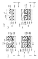
ここで、ローカル配線層部33におけるシングルダマシン構造を有する配線37−2及びビアプラグ37−1の構成について説明する。
図4(d)は、シングルダマシン構造を有する配線及びビアプラグの構成を示す断面図である。この配線及びビアプラグは、基板40上に設けられ、層間絶縁層3、キャップ絶縁層4、低誘電率絶縁層5、バリアメタル層8と導体部9とを含む第1配線10、キャップ絶縁層14、層間絶縁層15、バリアメタル層18と導体部19とを含むビア20、キャップ絶縁層24、低誘電率絶縁層25、バリアメタル層28と導体部29とを含む第2配線30を具備する。
【0058】
基板40は、複数の配線構造や素子が埋め込まれた絶縁膜の多層構造を有する半導体基板である。
【0059】
層間絶縁層3は、基板40を覆うように設けられている。CVD法やスピンコート法などで形成された絶縁膜である。配線間や配線と素子、素子間を絶縁する。配線の寄生容量を低減するために、低誘電率の材料を用いる。本実施例では、3.0以下の低い比誘電率を有する有機ポリマー系の低誘電率膜を用いる。
【0060】
キャップ絶縁層4は、層間絶縁層3を覆うように設けられている。層間絶縁膜3上に、CVD法やスピンコート法などで形成された絶縁膜である。第1配線10の配線溝を形成するフォトリソグラフィーのプロセスにおいて、層間絶縁膜3を保護する。本実施例では、炭化窒化シリコン(SiCN)である。膜厚は、例えば、およそ100nmである。
【0061】
低誘電率絶縁層5は、キャップ絶縁層4を覆うように設けられている。CVD法やスピンコート法などで形成された絶縁膜である。配線間や配線と素子、素子間を絶縁する。配線の寄生容量を低減するために、低誘電率の材料を用いる。本実施例においては、3.0以下の低い比誘電率を有する有機ポリマー系の低誘電率膜を用いる。膜厚は、例えば、およそ200nmである。
【0062】
第1配線10は、層間絶縁層3の表面からキャップ絶縁層4及び低誘電率絶縁層5を貫通する配線溝を埋めるように設けられている。バリアメタル層8と導体部9とを含む。
【0063】
バリアメタル層8は、配線溝の側壁及び底部を覆うように設けられている。スパッタ法により形成された金属薄膜である。導体部9が低誘電率絶縁層5へ拡散することや、導体部9が凝集することを防止する。高融点金属あるいはその窒化物である。本実施例では、タンタル/窒化タンタル(Ta/TaN)の積層膜である。膜厚は、例えば、およそ30nmである。
【0064】
導体部9は、バリアメタル層8を設けられた配線溝を満たす(埋める)ように設けられている。スパッタ法、メッキ法などにより形成された金属である。この部分は、コンタクト用に、抵抗率の低い金属で形成される。例えば、銅、銅−アルミニウムのような銅を含む金属である。本実施例では、銅(Cu)を用いる。第1配線10は、基板40と反対側の上部に、ビア20と接合する。第1配線10の深さ及び幅は、例えば、それぞれ300nm及び幅300nmである。
【0065】
キャップ絶縁層14は、低誘電率絶縁層5と第1配線10とを覆うように設けられている。材質、製法及び膜厚は、キャップ絶縁層4と同様である。
また、層間絶縁層15は、キャップ絶縁層14を覆うように設けられている。材質及び製法は、層間絶縁層3と同様である。膜厚は、例えば、およそ400nmである。
【0066】
バリアメタル層18は、ビアホール7の側壁及び底部を覆うように設けられている。材質、製法及び膜厚は、バリアメタル層8と同様である。
導体部19は、バリアメタル層18を設けられたビアホール7を満たす(埋める)ように設けられている。材質、及び製法は、導体部9と同様である。ビア32の大きさは、例えば、幅200nm、深さ500nmである。導体部19は、バリアメタル層18と共にビア20を形成する。
【0067】
キャップ絶縁層24は、層間絶縁層15を覆うように設けられている。材質、製法及び膜厚は、キャップ絶縁層4と同様である。
低誘電率絶縁層25は、キャップ絶縁膜24を覆うように設けられている。材質、製法及び膜厚は、低誘電率絶縁層5と同様である。
【0068】
バリアメタル層28は、層間絶縁層15及びビア20の表面からキャップ絶縁膜24及び低誘電率絶縁層25を貫通する配線溝17の側壁及び底部に設けられている。材質、製法及び膜厚は、バリアメタル膜8と同様である。ただし、配線溝17は、第2配線30を形成するための溝である。
導体部19は、バリアメタル膜28を設けられた配線溝17を満たす(埋める)ように設けられている。材質、製法及び膜厚は、導体部9と同様である。
【0069】
ここで、電源配線層部32におけるデュアルダマシン構造を有する配線34−2及びビアプラグ34−1の構成については、トレンチファースト法を用いているほかは、既述(図8から図11)のとおりなので、その説明を省略する。また、ビアファースト法を用いても良い。
ただし、電源配線層部32における層間絶縁層は、CVD法やスピンコート法などで形成された絶縁膜である。配線間を絶縁する。この部分の配線層は、配線間容量の影響が少ない。そのため、層間絶縁層は、二酸化シリコンに代表される無機系の絶縁膜を用いる。本実施例では、二酸化シリコンである。そのような絶縁層は、機械的な強度が強いため、組み立て時の半導体装置の損傷を防止することが出来る。
【0070】
本発明では、ローカル配線層部33において、デュアルダマシン構造を採用せず、銅のビアプラグを有するシングルダマシン構造を採用している。その理由を以下に説明する。
【0071】
デュアルダマシン構造を有するローカル配線層部33をビアファースト法により作成する従来の場合、図9(a)及び(c)の工程において、近傍に他のビアホールが無い孤立したビアホール(以下「孤立ビアホール」という)と、近傍に他のビアホールが多く密集したビアホール(以下「密集ビアホール」という)とでは、詰め込まれるARC(Anti−Reflection Coating:有機物142)の厚さ(高さ:図9(a)及び(c)のhA)が変わってくる。それは、以下の理由による。同一配線層上には、配線層の表面の単位面積あたり、一定のARCが供給される。そのため、周辺に他のビアホールが無い孤立ビアホールには多くのARCが詰め込まれる。しかし、周辺に他の多くのビアホールがある密集ビアホールには、孤立ビアホールに詰め込まれるよりも少なくARCが詰め込まれることになる。
【0072】
このような場合、詰め込まれるARCの高さhAの上限を、孤立ビアホールでの高さで律速することとする。すなわち、図12に示すようなフェンス145の形成を防止するために、孤立ビアホールのある部分では、詰め込まれるARCの高さhAは異層間の絶縁層(図12等におけるストッパ絶縁層124+層間絶縁層115)の膜厚h以下となるようにする。その場合、同じ配線層にある密集ビアホールにおいて、異層間の絶縁層の膜厚をh(μm)、単位面積あたりの密集ビアホールの個数(=単位面積あたりのビアプラグの個数、以下「ビア密度」ともいう)をn(個/μm2)とすると、ここでの詰め込みARCの高さhAは、おおむねh/nとなる。配線の最小ピッチをL(μm)とすると密集ビアホールのピッチは、L(μm)となる。このようなビアホールでビアプラグを作製した場合、図14(b)に示すような肩落ち部が形成される。その状態を改めて示したのが、図5(b)及び(d)である。
【0073】
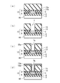
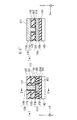
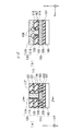
図5は、シングルマシン構造の配線及びビアプラグ((a)及び(c))と、ビアファースト法によるデュアルダマシン構造の配線及びビアプラグ((b)及び(d))を示す半導体装置の断面図である。図5(a)及び図5(b)は側面図、図5(c)及び図5(d)は上面図である。
図5(b)を参照して、このデュアルダマシン構造は、第1層の配線51とビアプラグ52と第2層の配線53と肩落ち部55を備えている。配線51及び配線53は、膜厚t(μm)、ビアプラグ52は、高さh(μm)である。また、上記の議論から肩落ち部55の高さ(=詰め込みARCの高さhA)は、おおむねh/nとなる。
【0074】
ここで、図5(d)を参照して、配線53(肩落ち部55を含む)−ビアプラグ52−配線51−ビアプラグ52−配線53(肩落ち部55を含む)の組に対して、同様の配線53a(肩落ち部55aを含む)−ビアプラグ52a−配線51a−ビアプラグ52a−配線53a(肩落ち部55aを含む)の組が、平行に設けられている場合を考える。このような構造は、DRAMやSRAMのようなメモリに例示される半導体装置に典型的に見られる構造である。
配線ピッチをL(μm)、配線幅をL/2(μm)、配線間の距離をL/2(μm)とすれば、点線で囲まれた部分の配線間容量(CD/ε:εは異層間の絶縁層の誘電率)は、
(A)デュアルダマシン構造の場合

【0075】
一方、図5(a)を参照して、このシングルダマシン構造では、第1層の配線41とビアプラグ42と第2層の配線43とを備えている。配線41及び配線43は、膜厚t(μm)、ビアプラグ42は、高さh(μm)である。
ここで、図5(c)を参照して、図5(d)の場合と同様に、配線43−ビアプラグ42−配線41−ビアプラグ42−配線43の組に対して、同様の配線43a−ビアプラグ42a−配線41a−ビアプラグ42a−配線43aの組が、平行に設けられている場合を考える。配線ピッチをL(μm)、配線幅をL/2(μm)、配線間の距離をL/2(μm)とすれば、点線で囲まれた部分の配線間容量(CS/ε:εは異層間の絶縁層の誘電率)は、
(B)シングルダマシン構造の場合
【0076】
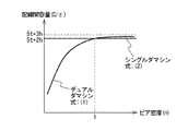
図6は、式(1)及び式(2)を示すグラフである。縦軸は配線間容量(C/ε)、横軸はビア密度nである。ビア密度nが増加する、すなわちビアプラグ間のピッチが狭くなると、デュアルダマシンの場合、配線容量が増加する。しかし、シングルダマシンの場合、配線容量はビア密度によらない。つまり、配線間容量がシングルダマシンの場合の値に比較して大きくなるようなビア密度nで、シングルダマシン法を採用すればよい。
【0077】
図6及び式(1)及び式(2)から、n=1以上の場合、シングルダマシン構造での配線間容量が、デュアルダマシン構造のそれを下回ることがわかる。すなわち、ビア密度nは、n≧1が好ましい。この場合、ピッチは、無関係である。さらに、DRAMやSRAMのようなメモリに例示される半導体装置に平均的な値として、t=0.3μm、h=0.4μmを用い、設計の要請から配線間容量を0.18fF/μm以下にする場合、n≧25となり、ピッチは、0.4μmとなる。
【0078】
本発明により、半導体装置のローカル配線層部での配線が微細化してビア密度nが大きくなる場合でも、シングルダマシン構造を採用することにより、デュアルダマシン構造の場合に比較して配線間容量を抑えることが可能となる。
【0079】
次に、本発明の半導体装置の製造方法について説明する。
まず、ローカル配線層部33の製造方法について説明する。ここでは、シングルダマシン構造を有する一配線層33−1分の配線及びビアプラグを製造する方法について説明する。図2〜図4は、シングルダマシン構造を構成する配線及びビアプラグの製造方法を示す半導体装置の断面図である。ここでは、2つの層のそれぞれに設けられた配線と、それらを繋ぐビアプラグとを形成する例を示す。
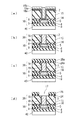
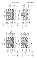
【0080】
図2において、複数の半導体素子を設けられた基板40上に、層間絶縁膜3上のストッパ絶縁層4及び低誘電率絶縁層5の中に、第1層の配線10が設けられる。配線10は、銅(Cu)の配線9とタンタル/窒化タンタル(Ta/TaN)のバリアメタル層8とを含み、ダマシン構造を有する。従来知られた配線製造プロセスで設けられる。そして、配線10と低誘電率絶縁層5とを覆うようにストッパ絶縁膜14aが設けられる。更に、ストッパ絶縁膜14aを覆うように層間絶縁膜15aが設けられる。この、図2(a)の状態において、フォトリソグラフィーのプロセスを用いて、ストッパ絶縁膜14aと層間絶縁膜15aとにビアホール7を形成する。ビアホール7を形成されたストッパ絶縁膜14aと層間絶縁膜15aを、それぞれ、ストッパ絶縁層14と層間絶縁層15とする。この図2(b)の状態において、層間絶縁層5の表面とビアホール7の側壁(側面)及び底部とを覆うように、Ta/TaNからなるバリアメタル膜18aをスパッタ法で設ける。このときビアホール7aとなる。この図2(c)の状態において、バリアメタル膜18aを覆うようにCuからなるシード導体膜19aを設ける。このときビアホール7bとなる。この状態が図2(d)である。
【0081】
次に、図2(d)の状態において、シード導体膜19aを覆い、且つ、ビアホール7bを埋めるようにCuからなる導体膜19bを設ける。この図3(a)の状態において、層間絶縁層15表面及びビアホール7上方における不要なバリアメタル膜18a、シード導体膜19a及び導体膜19bをCMP(Chemical Mechanical Polishing)で除去する。このようにして、バリアメタル層18及び導体層19とからなるビアプラグ20(コンタクト)が形成される。この図3(b)の状態において、ビアプラグ20と層間絶縁膜15とを覆うようにストッパ絶縁膜24aが設けられる。更に、ストッパ絶縁膜24aを覆うように低誘電率絶縁膜25aが設けられる。この図3(c)の状態において、フォトリソグラフィーのプロセスを用いて、ストッパ絶縁膜24aと低誘電率絶縁膜25aとに第2層の配線溝17を形成する。このとき、配線溝17を形成されたストッパ絶縁膜24aと低誘電率絶縁膜25aを、それぞれ、ストッパ絶縁層24と低誘電率絶縁層25とする。この状態が図3(d)である。
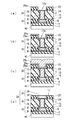
【0082】
次に、図3(d)の状態において、低誘電率絶縁層25と配線溝17の側壁及び底部とを覆うように、Ta/TaNからなるバリアメタル膜28aをスパッタ法で設ける。このとき配線溝17aとなる。この図4(a)の状態において、バリアメタル膜28aを覆うようにCuからなるシード導体膜29aを設ける。このとき配線溝17bとなる。この図4(b)の状態において、シード導体膜29aを覆い、且つ、ビアプラグ17を埋めるようにCuからなる導体膜29bを設ける。この図4(c)の状態において、低誘電率絶縁層25表面及び配線溝17上方における不要なバリアメタル膜28a、シード絶縁膜29a及び導体膜29bをCMPで除去する。このようにして、バリアメタル層28及び導体層29とからなる配線30が形成される。配線30及びビアプラグ20は、接合体38(図1、シングルダマシン法で形成)に対応する。
【0083】
そして、以上の図2〜図4の製造方法により、シングルダマシン構造を有する一配線層33−1分の配線及びビアプラグが形成される。ただし、図4におけるビアプラグ20、配線10及び配線30は、それぞれ図1におけるビアプラグ37−1、配線37−2に対応する。積層された他の配線層33−1も同様にして形成できる。
【0084】
ビアプラグ36の製造方法については、上述のシングルダマシン法又は従来のデュアルダマシン法を用いて形成できるのでその説明を省略する。また、電源配線層部32の製造方法については、層間絶縁層に二酸化シリコンに代表される無機系の絶縁膜を用いる他は、既述のデュアルダマシン法(トレンチファースト法)を用いて形成しているのでその説明を省略する。
【0085】
本発明では、シングルダマシン構造を採用することにより、微細な配線の形成を安定して行うことができる。それにより、配線のピッチが短く配線が微細なローカル配線部において、バリアメタル膜を厚くつける必要がなくなり、配線の抵抗を低減することが出来る。
【0086】
更に、電源配線層部では、デュアルダマシン構造を採用しているので、ビアプラグの抵抗を低く保ち、その工程数を少なく維持できる。
【0087】
加えて、電源配線層部における層間絶縁層は、二酸化シリコンに代表される無機系の絶縁膜を用いるので、機械的な強度が強く、組み立て時の半導体装置の損傷を防止することが出来る。
【0088】
【発明の効果】
本発明により、半導体装置のローカル配線層部での配線が微細化してビア密度nが大きくなる場合でも、シングルダマシン構造を採用することにより、デュアルダマシン構造の場合に比較して配線間容量を抑えることが可能となる。
【図面の簡単な説明】
【図1】図1は、本発明の半導体装置の配線に関わる構造を示す断面図である。
【図2】図2は、シングルダマシン構造を構成する配線及びビアプラグの製造方法を示す半導体装置の断面図である。
【図3】図3は、シングルダマシン構造を構成する配線及びビアプラグの製造方法を示す半導体装置の断面図である。
【図4】図4は、シングルダマシン構造を構成する配線及びビアプラグの製造方法を示す半導体装置の断面図である。
【図5】図5は、シングルマシン構造及びデュアルダマシン構造の配線及びビアプラグを示す半導体装置の断面図である。
【図6】図6は、式(1)及び式(2)を示すグラフである。
【図7】図7は、半導体装置の配線に関わる構造を示す半導体装置の断面図である。
【図8】図8は、ビアファースト法のプロセスを示す半導体装置の断面図である。
【図9】図9は、ビアファースト法のプロセスを示す半導体装置の断面図である。
【図10】図10は、ビアファースト法のプロセスを示す半導体装置の断面図である。
【図11】図11は、ビアファースト法のプロセスを示す半導体装置の断面図である。
【図12】図12は、ビアホールを完全に埋めるように有機物を入れた場合の半導体装置の断面を示す図である。
【図13】図13は、有機物の量をストッパ絶縁層の高さよりも低くした場合の半導体装置の断面図である。
【図14】図14は、有機物の量をストッパ絶縁層の高さよりも低くした場合の半導体装置の断面図である。
【図15】図15は、図13及び図14の肩落ちを含む半導体装置の配線に関わる構造を示す断面図である。
【符号の説明】
1、101、101a 半導体装置
3、15、103、115 層間絶縁層
15a、115a 層間絶縁膜
4、14、24、104、114、124 ストッパ絶縁層
14a、24a、114a、124a ストッパ絶縁膜
5、25、105、125 低誘電率絶縁層
25a、125a 低誘電率絶縁膜
7、7a、7b、107、107a(’)、107b、107c ビアホール
8、18、28、118 バリアメタル層
18a、28a、118a バリアメタル膜
9、19、29、119 導体部
19a、29a、119a シード導体膜
19b、29b、129a 導体膜
10、30、41、43、51、53、110 配線
17、17a、17b、117(’) 配線溝
20、42、52、120 ビアプラグ
30、130 ビアプラグ
31、131、131a 素子部
32、132、132a 電源配線層部
32−1、132−1、132a−1 配線層
33、133、133a ローカル配線層部
33−1、133−1、133a−1 配線層
34−1、37−1、134−1、137−1、134a−1、137a−1 ビアプラグ
34−2、37−2、134−2、137−2、134a−2、137a−2 配線
35、38、135、138、135a、138a 接合部
36、136、136a ビアプラグ
40、140、140a 基板
142(’、’’) 有機物
146、146a 肩落ち部[0001]
TECHNICAL FIELD OF THE INVENTION
The present invention relates to a semiconductor device and a method of manufacturing a semiconductor device, and more particularly, to a semiconductor device including a wiring having a damascene structure made of metal including copper and a via plug, and a method of manufacturing the semiconductor device.
[0002]
[Prior art]
As a structure related to wiring of a semiconductor device, a structure in which a local wiring layer portion and a power supply wiring layer portion are sequentially stacked on a plurality of elements provided on a semiconductor substrate is known. In such a semiconductor device, copper (Cu) is generally used as a material for wiring in each layer, and tungsten (W) is generally used as a material for via plugs used for connection between layers.
[0003]
However, since the film formation temperature of tungsten is extremely high, copper in miniaturized wiring cannot withstand, aggregation occurs, and the probability of disconnection increases. On the other hand, via plugs using copper have advantages such as lower via resistance and higher resistance to thermal stress than via plugs using tungsten. For these reasons, copper is increasingly used in via plugs in recent years.
[0004]
There are a dual damascene method and a single damascene method as a method for forming both the wiring and the via plug with copper. The dual damascene method has advantages over the single damascene method in that the number of CMP steps is one less, and the wiring resistance is low because a barrier metal film is not interposed between the wiring and the via plug. Therefore, at present, all wirings and via plugs are often formed by a dual damascene method. The structure of such a semiconductor device will be described with reference to FIG.
[0005]
FIG. 7 is a cross-sectional view illustrating a structure related to wiring of the semiconductor device. The
[0006]
The local
The
[0007]
The power
[0008]
Here, the dual damascene method includes a via first method and a trench first method. In the via-first method, it is necessary to fill a via hole with BARC (Bottom Anti-Reflection Coating) after opening the via hole and before forming a wiring groove (trench) in order to prevent reflection during exposure. Therefore, the process becomes complicated. Therefore, the trench first method with few steps is preferably used.
[0009]
However, in the trench-first method, when forming a via hole by photolithography, it is necessary to apply a resist on a semiconductor device having a step of a wiring groove (trench) and expose a predetermined pattern. Therefore, depending on the pattern of the wiring groove, it is difficult to properly focus on the surface due to the step. In particular, a fine shape cannot be exposed accurately. Therefore, it is common to form a via hole by a via-first method in a place where the size of a via plug such as the local
[0010]
Hereinafter, a via-first method which is one of the dual damascene methods will be described. 8 to 11 are cross-sectional views of a semiconductor device showing a process of the via-first method. Here, an example is shown in which wirings provided in each of two layers and via plugs connecting them are formed.
[0011]
As shown in FIG. 8A, a
[0012]
Subsequently, from the state of FIG. 8A, a
[0013]
Next, an organic substance 142 (for example, BARC) is embedded in the
[0014]
Subsequently, from the states of FIGS. 9A and 9C, a
[0015]
Next, the
[0016]
Subsequently, from the state of FIGS. 10A and 10C, the surface of the low-dielectric-constant
[0017]
Next, from the states shown in FIGS. 10B and 10D, unnecessary
[0018]
As described above, the wiring and the via plug are formed by the via-first method, which is one of the dual damascene methods, by the manufacturing method of FIGS. However, the via
[0019]
In the trench first method, which is one of the dual damascene methods used for the power
[0020]
As a related technique, Japanese Patent Application Laid-Open No. 2001-156168 (Patent Document 1) discloses a technique of a semiconductor device and a method of manufacturing the same. A semiconductor device according to this technique has a semiconductor substrate and a plurality of wiring layers. The semiconductor substrate has a plurality of elements formed thereon. A plurality of wiring layers are formed on the semiconductor substrate. The plurality of wiring layers include a signal line made of copper for connecting the plurality of elements, a power supply line made of copper for supplying power to the plurality of elements, and a ground line. The connection of the signal line, the power supply line, and the ground line between the plurality of wiring layers is performed by vias formed below the signal line, the power supply line, and the ground line. Here, the signal line and the first via formed below the signal line are formed by a single damascene process using tungsten for the via. The power supply line and the ground line, and the second via formed below the power supply line and the ground line are formed by a dual damascene process. The area of the second via is formed to be larger than the area of the first via by a preset ratio.
The purpose of this technique is to provide a semiconductor device having high mechanical strength and excellent heat dissipation, and a method for manufacturing the same.
[0021]
[Patent Document 1]
JP 2001-156168 A (FIG. 1B, FIG. 6, FIG. 7, FIG. 8)
[0022]
[Problems to be solved by the invention]
9B and 9D, the uppermost position of the
[0023]
If the uppermost position of the
[0024]
FIG. 12 is a diagram showing a cross section of the semiconductor device in a case where an organic substance is introduced so that the uppermost position of the organic substance is higher than the position of the stopper insulating film. FIG. 12A corresponds to FIG. FIG. 12C is a cross-sectional view taken along the line FF ′ of FIG. The organic substance 142 'is embedded up to the level of the low dielectric
[0025]
On the other hand, if the uppermost position of the
[0026]
FIG. 13 is a cross-sectional view of a semiconductor device in which an organic substance is placed so that the uppermost position of the organic substance is lower than the position of the stopper insulating film. FIG. 13A corresponds to FIG. FIG. 13C is a cross section taken along line HH ′ of FIG. The via
[0027]
Thereafter, the
[0028]
In recent years, with progress in miniaturization of semiconductor devices, it is important to maintain the reliability of wiring. Specifically, a thick barrier metal film is formed to prevent migration of copper and diffusion into the insulating film. For the reason described with reference to FIG. 12, the organic material to be embedded in the via hole is not increased and the height is lower than the height of the cap insulating layer. It is necessary to do. In this case, the resistance of the wiring increases due to the thick barrier metal film, and the formation of the shoulder drop-
[0029]
FIG. 15 is a cross-sectional view showing a structure related to the wiring of the semiconductor device including the shoulder drop of FIGS. 13 and 14. The
[0030]
In this case, the pitch of the via plug 137a-1 is small, and the distance between the individual
[0031]
There is a demand for a technique for improving the reliability of wiring and via plugs in a local wiring layer in a semiconductor device. There is a need for a technique for preventing an increase in inter-wiring capacitance. There is a demand for a technique for preventing an increase in wiring resistance. There is a need for a technique capable of keeping the resistance of a via plug in a power supply wiring layer low and reducing the number of steps.
[0032]
SUMMARY OF THE INVENTION It is therefore an object of the present invention to provide a semiconductor device and a method of manufacturing a semiconductor device that improve the reliability of wiring and via plugs in a local wiring layer.
[0033]
Another object of the present invention is to provide a semiconductor device and a method of manufacturing a semiconductor device, which prevent an increase in inter-wiring capacitance and wiring resistance in a local wiring layer portion.
[0034]
Still another object of the present invention is to provide a semiconductor device and a method of manufacturing the semiconductor device, which can improve the reliability of operation.
[0035]
Another object of the present invention is to provide a semiconductor device and a method of manufacturing the semiconductor device, which can keep the resistance of a via plug in a power supply wiring layer portion low and reduce the number of steps.
[0036]
[Means for Solving the Problems]
The means for solving the problem will be described below using the numbers and symbols used in [Embodiments of the Invention]. These numbers and symbols have been added in order to clarify the correspondence between the description of [Claims] and [Embodiments of the Invention]. However, those numbers and symbols must not be used for interpreting the technical scope of the invention described in [Claims].
[0037]
Therefore, in order to solve the above problems, the semiconductor device of the present invention is formed on the first wiring layer portion (33) formed on the semiconductor substrate (40) and on the first wiring layer portion (33). A second wiring layer (32). The first wiring layer (33) has a first interlayer insulating film, a plurality of first via plugs (37-1), and a plurality of first wirings (37-2). The plurality of first via plugs (37-1) are provided in the first interlayer insulating film and are separated from each other by a first distance or more. The plurality of first wirings (37-2) are provided on the plurality of first via plugs (37-1) in the first interlayer insulating film and are connected to the plurality of first via plugs (37-1). The second wiring layer (32) has a second interlayer insulating film, a plurality of second via plugs (34-1), and a plurality of second wirings (34-2). The plurality of second via plugs (34-1) are provided in the second interlayer insulating film and are separated from each other by a second interval or more that is greater than the first interval. The plurality of second wirings (34-2) are provided on the plurality of second via plugs (34-1) in the second interlayer insulating film and are connected to the plurality of second via plugs (34-1). The plurality of first via plugs (37-1), the plurality of first wirings (37-2), the plurality of second via plugs (34-1), and the plurality of second wirings (34-2) are made of metal containing copper. Become. The first wiring layer (33) has a single damascene structure, and the second wiring layer (32) has a dual damascene structure.
[0038]
According to the present invention, by adopting a single damascene structure in the first wiring layer portion (33) in which the distance between via plugs is smaller than that in the second wiring layer portion (32) of the semiconductor device, the shoulder drop portion (146) shown in FIG. ) Can be prevented. This makes it possible to reduce the capacitance between wirings as compared with the case of the dual damascene structure.
[0039]
In the above-described semiconductor device, the first wiring layer (33) includes a plurality of first via plugs (37-1) and a plurality of first wirings (37-2) provided in the first interlayer insulating film. Including a plurality of layers. The second wiring layer (32) includes a plurality of layers including a plurality of second via plugs (34-1) and a plurality of second wirings (34-2) provided in the second interlayer insulating film. .
[0040]
In the above-described semiconductor device, the first interval is set such that the via density (n) as the number of via plugs per unit area for the plurality of first via plugs (37-1) satisfies a predetermined condition. The predetermined condition is that the inter-wiring capacitance (C) between each of the plurality of first wirings (37-2). S ) Is the case where the first wiring layer portion (33) is formed by the dual damascene method (C D ) Is smaller.
[0041]
As the via density (n) increases, the influence of the shoulder drop portion (146) by the dual damascene method increases. In the present invention, in such a situation (predetermined condition) where the influence occurs, the single damascene method is used. Therefore, it is possible to prevent an increase in capacitance between wirings.
[0042]
In the above semiconductor device, the via density (n) is 1 piece / μm 2 That is all.
The influence of the shoulder drop portion (146) is particularly caused when the via density (n) is 1 piece / μm. 2 As described above, by applying the present invention to the range, an increase in the capacitance between wirings can be prevented.
[0043]
In the above-described semiconductor device, the first interval is 0.5 μm.
By applying the present invention to that range, an increase in the capacitance between wirings can be prevented.
[0044]
In the above-described semiconductor device, each of the plurality of first via plugs (37-1) has a diameter of 0.4 μm or less.
When the diameter of each of the first via plugs (37-1) is 0.4 μm or less, particularly, the via-first method is used. Therefore, by applying the present invention to the range, it is possible to prevent an increase in the capacitance between wirings. it can.
[0045]
In order to solve the above problems, a method of manufacturing a semiconductor device according to the present invention includes steps (a) to (f). (A) is a step of forming a first insulating film on a semiconductor substrate (40). (B) is a step of forming a plurality of first via plugs (37-1) made of a metal containing copper and separated from each other at a first interval or more by a single damascene method in the first insulating film. (C) is a step of forming a second insulating film on the first insulating film and the plurality of first via plugs (37-1). (D) is a step of forming a plurality of first wirings (37-2) made of a metal containing copper connected to the plurality of first via plugs (37-1) on the second insulating film by a single damascene method. is there. (E) is a step of forming a third insulating film on the second insulating film and the plurality of first wirings (37-2). (F) is connected to the plurality of second via plugs (34-1) and the plurality of second via plugs (34-1) separated from each other by the third insulating film at a second interval larger than the first interval. Forming a plurality of second wirings (34-2) made of a metal containing copper by a dual damascene method.
[0046]
In the above method for manufacturing a semiconductor device, the dual damascene method is a trench first method.
[0047]
The method for manufacturing a semiconductor device described above further includes steps (g) to (h). (G) is a step of repeating the steps (a) to (d) for a desired number of layers between the steps (d) and (e). (H) is a step of repeating the steps (e) to (f) for the desired number of layers after the step (f).
[0048]
In the above-described method for manufacturing a semiconductor device, the first interval is set such that the via density (n) as the number of via plugs per unit area for the plurality of first via plugs (37-1) satisfies a predetermined condition. Is done. The predetermined condition is that the inter-wiring capacitance (C) between each of the plurality of first wirings (37-2). S ), When a plurality of first via plugs (37-1) and a plurality of first wirings (37-2) are formed by a dual damascene method (C). D ) Is smaller.
[0049]
In the above method for manufacturing a semiconductor device, the via density (n) is 1 / μm 2 That is all.
[0050]
In the above-described method for manufacturing a semiconductor device, the first interval is 0.5 μm.
[0051]
In the above method for manufacturing a semiconductor device, each of the plurality of first via plugs (37-1) has a diameter of 0.4 μm or less.
[0052]
BEST MODE FOR CARRYING OUT THE INVENTION
Hereinafter, embodiments of a semiconductor device and a method of manufacturing a semiconductor device according to the present invention will be described with reference to the accompanying drawings.
[0053]
First, the configuration of the embodiment of the semiconductor device of the present invention will be described.
FIG. 1 is a cross-sectional view showing a structure related to wiring of a semiconductor device of the present invention. The
[0054]
The
[0055]
The local
[0056]
The power supply wiring layer portion 32 is provided on the local
[0057]
Here, the configuration of the wiring 37-2 having a single damascene structure and the via plug 37-1 in the
FIG. 4D is a cross-sectional view illustrating a configuration of a wiring and a via plug having a single damascene structure. These wirings and via plugs are provided on a
[0058]
The
[0059]
The interlayer insulating
[0060]
The
[0061]
The low dielectric constant insulating
[0062]
The
[0063]
The
[0064]
The
[0065]
The
The interlayer insulating
[0066]
The
The
[0067]
The
The low dielectric constant insulating
[0068]
The
The
[0069]
Here, the configuration of the wiring 34-2 and the via plug 34-1 having the dual damascene structure in the power supply wiring layer portion 32 is as described above (FIGS. 8 to 11) except that the trench first method is used. , The description of which will be omitted. Further, a via-first method may be used.
However, the interlayer insulating layer in the power supply wiring layer section 32 is an insulating film formed by a CVD method, a spin coating method, or the like. Insulate between wiring. The wiring layer in this portion is less affected by the capacitance between wirings. Therefore, an inorganic insulating film represented by silicon dioxide is used for the interlayer insulating layer. In this embodiment, it is silicon dioxide. Since such an insulating layer has high mechanical strength, damage to the semiconductor device during assembly can be prevented.
[0070]
In the present invention, the
[0071]
In the conventional case where the
[0072]
In such a case, the height h of the ARC to be packed is A Is limited by the height of the isolated via hole. That is, in order to prevent the formation of the
[0073]
FIG. 5 is a cross-sectional view of a semiconductor device showing wiring and via plugs ((a) and (c)) having a single machine structure and wiring and via plugs ((b) and (d)) having a dual damascene structure by a via-first method. is there. 5 (a) and 5 (b) are side views, and FIGS. 5 (c) and 5 (d) are top views.
Referring to FIG. 5B, this dual damascene structure includes a
[0074]
Here, referring to FIG. 5D, the same applies to a set of wiring 53 (including shoulder drop-down portion 55), via
If the wiring pitch is L (μm), the wiring width is L / 2 (μm), and the distance between the wirings is L / 2 (μm), the capacitance between wirings (C D / Ε: ε is the dielectric constant of the insulating layer between different layers)
(A) Dual damascene structure
[0075]
On the other hand, referring to FIG. 5A, this single damascene structure includes a first-
Here, referring to FIG. 5 (c), similar to the case of FIG. 5 (d), the
(B) Single damascene structure
[0076]
FIG. 6 is a graph showing Expression (1) and Expression (2). The vertical axis represents the capacitance between wirings (C / ε), and the horizontal axis represents the via density n. When the via density n increases, that is, when the pitch between the via plugs decreases, the wiring capacity increases in the case of dual damascene. However, in the case of a single damascene, the wiring capacity does not depend on the via density. In other words, the single damascene method may be employed at a via density n such that the inter-wiring capacitance is larger than that in the case of single damascene.
[0077]
From FIG. 6 and Expressions (1) and (2), it can be seen that when n = 1 or more, the inter-wiring capacitance in the single damascene structure is lower than that in the dual damascene structure. That is, the via density n is preferably n ≧ 1. In this case, the pitch is irrelevant. Further, t = 0.3 μm and h = 0.4 μm are used as average values for semiconductor devices exemplified by memories such as DRAM and SRAM, and the capacitance between wirings is set to 0.18 fF / μm or less due to design requirements. In this case, n ≧ 25, and the pitch is 0.4 μm.
[0078]
According to the present invention, even when the wiring in the local wiring layer portion of the semiconductor device is miniaturized and the via density n increases, the capacitance between the wirings is suppressed by adopting the single damascene structure as compared with the dual damascene structure. It becomes possible.
[0079]
Next, a method for manufacturing a semiconductor device of the present invention will be described.
First, a method for manufacturing the
[0080]
In FIG. 2, a
[0081]
Next, in the state of FIG. 2D, a
[0082]
Next, in the state of FIG. 3D, a
[0083]
Then, the wiring and the via plug for one wiring layer 33-1 having the single damascene structure are formed by the manufacturing method of FIGS. 1. However, the via
[0084]
The method of manufacturing the via
[0085]
In the present invention, by employing a single damascene structure, fine wiring can be formed stably. This eliminates the need to thicken the barrier metal film in the local wiring portion where the wiring pitch is short and the wiring is fine, and the resistance of the wiring can be reduced.
[0086]
Further, since the power supply wiring layer has a dual damascene structure, the resistance of the via plug can be kept low, and the number of steps can be kept low.
[0087]
In addition, since an inorganic insulating film typified by silicon dioxide is used for the interlayer insulating layer in the power supply wiring layer portion, the mechanical strength is high, and damage to the semiconductor device during assembly can be prevented.
[0088]
【The invention's effect】
According to the present invention, even when the wiring in the local wiring layer portion of the semiconductor device is miniaturized and the via density n increases, the capacitance between the wirings is suppressed by adopting the single damascene structure as compared with the dual damascene structure. It becomes possible.
[Brief description of the drawings]
FIG. 1 is a cross-sectional view showing a structure related to wiring of a semiconductor device of the present invention.
FIG. 2 is a cross-sectional view of the semiconductor device illustrating a method of manufacturing a wiring and a via plug forming a single damascene structure.
FIG. 3 is a cross-sectional view of the semiconductor device illustrating a method of manufacturing a wiring and a via plug forming a single damascene structure.
FIG. 4 is a cross-sectional view of the semiconductor device illustrating a method of manufacturing a wiring and a via plug forming a single damascene structure.
FIG. 5 is a cross-sectional view of a semiconductor device showing wiring and via plugs having a single-machine structure and a dual-damascene structure.
FIG. 6 is a graph showing Expressions (1) and (2).
FIG. 7 is a cross-sectional view of the semiconductor device showing a structure related to wiring of the semiconductor device;
FIG. 8 is a sectional view of the semiconductor device showing a process of a via-first method.
FIG. 9 is a cross-sectional view of the semiconductor device illustrating a process of a via-first method.
FIG. 10 is a cross-sectional view of the semiconductor device illustrating a process of a via-first method.
FIG. 11 is a cross-sectional view of the semiconductor device illustrating a process of a via-first method.
FIG. 12 is a diagram showing a cross section of a semiconductor device in a case where an organic substance is filled so as to completely fill a via hole.
FIG. 13 is a cross-sectional view of the semiconductor device when the amount of the organic substance is lower than the height of the stopper insulating layer.
FIG. 14 is a cross-sectional view of the semiconductor device when the amount of an organic substance is lower than the height of a stopper insulating layer.
FIG. 15 is a cross-sectional view showing a structure related to wiring of the semiconductor device including the shoulder drop of FIGS. 13 and 14;
[Explanation of symbols]
1, 101, 101a Semiconductor device
3, 15, 103, 115 interlayer insulating layer
15a, 115a interlayer insulating film
4, 14, 24, 104, 114, 124 Stopper insulating layer
14a, 24a, 114a, 124a Stopper insulating film
5, 25, 105, 125 Low dielectric constant insulating layer
25a, 125a Low dielectric constant insulating film
7, 7a, 7b, 107, 107a ('), 107b, 107c Via hole
8, 18, 28, 118 Barrier metal layer
18a, 28a, 118a Barrier metal film
9, 19, 29, 119 conductor
19a, 29a, 119a Seed conductor film
19b, 29b, 129a Conductive film
10, 30, 41, 43, 51, 53, 110 wiring
17, 17a, 17b, 117 (') wiring groove
20, 42, 52, 120 Via plug
30, 130 via plug
31, 131, 131a Element section
32, 132, 132a Power supply wiring layer
32-1, 132-1, 132a-1 wiring layer
33, 133, 133a Local wiring layer
33-1, 133-1, 133a-1 Wiring layer
34-1, 37-1, 134-1, 137-1, 134a-1, 137a-1 Via plug
34-2, 37-2, 134-2, 137-2, 134a-2, 137a-2 Wiring
35, 38, 135, 138, 135a, 138a Joint
36,136,136a Via plug
40, 140, 140a substrate
142 (','') organic matter
146, 146a shoulder drop
Claims (13)
前記第1配線層部上に形成された第2配線層部と
を具備し、
前記第1配線層部は、
第1層間絶縁膜と、
前記第1層間絶縁膜内に設けられ第1間隔以上で互いに隔てられた複数の第1ビアプラグと、
前記第1層間絶縁膜内において前記複数の第1ビアプラグ上に設けられ前記複数の第1ビアプラグに接続された複数の第1配線と
を有し、
前記第2配線層部は、
第2層間絶縁膜と、
前記第2層間絶縁膜内に設けられ前記第1間隔よりも大きい第2間隔以上で互いに隔てられた複数の第2ビアプラグと、
前記第2層間絶縁膜内において前記複数の第2ビアプラグ上に設けられ前記複数の第2ビアプラグに接続された複数の第2配線と
を有し、
前記複数の第1ビアプラグ、前記複数の第1配線、前記複数の第2ビアプラグ及び前記複数の第2配線は、銅を含む金属からなり、
前記第1配線層部は、シングルダマシン構造であり、
前記第2配線層部は、デュアルダマシン構造である
半導体装置。A first wiring layer formed on the semiconductor substrate;
A second wiring layer portion formed on the first wiring layer portion,
The first wiring layer section includes:
A first interlayer insulating film;
A plurality of first via plugs provided in the first interlayer insulating film and separated from each other by a first distance or more;
A plurality of first wirings provided on the plurality of first via plugs in the first interlayer insulating film and connected to the plurality of first via plugs;
The second wiring layer portion includes:
A second interlayer insulating film;
A plurality of second via plugs provided in the second interlayer insulating film and separated from each other by a second interval or more that is larger than the first interval;
A plurality of second wirings provided on the plurality of second via plugs in the second interlayer insulating film and connected to the plurality of second via plugs;
The plurality of first via plugs, the plurality of first wirings, the plurality of second via plugs, and the plurality of second wirings are made of a metal including copper,
The first wiring layer has a single damascene structure,
The semiconductor device, wherein the second wiring layer has a dual damascene structure.
前記第1配線層部は、前記第1層間絶縁膜内に設けられた前記複数の第1ビアプラグと前記複数の第1配線とを含む複数の層を備え、
前記第2配線層部は、前記第2層間絶縁膜内に設けられた前記複数の第2ビアプラグと前記複数の第2配線とを含む複数の層を備える
半導体装置。The semiconductor device according to claim 1,
The first wiring layer portion includes a plurality of layers including the plurality of first via plugs provided in the first interlayer insulating film and the plurality of first wirings,
The semiconductor device, wherein the second wiring layer portion includes a plurality of layers including the plurality of second via plugs and the plurality of second wirings provided in the second interlayer insulating film.
前記第1間隔は、前記複数の第1ビアプラグに関する単位面積あたりのビアプラグの個数としてのビア密度が、所定の条件を満たすように設定され、
前記所定の条件は、前記複数の第1配線の各々間の配線間容量が、前記第1配線層部をデュアルダマシン法で形成した場合に比較して、小さくなることである
半導体装置。The semiconductor device according to claim 1, wherein
The first interval is set such that a via density as the number of via plugs per unit area for the plurality of first via plugs satisfies a predetermined condition;
The predetermined condition is that the inter-wiring capacitance between each of the plurality of first wirings is smaller than when the first wiring layer is formed by a dual damascene method.
前記ビア密度は、1個/μm2以上である
半導体装置。The semiconductor device according to claim 3,
The semiconductor device, wherein the via density is 1 / μm 2 or more.
前記第1間隔は、0.5μmである
半導体装置。The semiconductor device according to claim 3, wherein
The semiconductor device, wherein the first interval is 0.5 μm.
前記複数の第1ビアプラグの各々の直径は、0.4μm以下である
半導体装置。The semiconductor device according to claim 1, wherein
The semiconductor device, wherein each of the plurality of first via plugs has a diameter of 0.4 μm or less.
(b)前記第1絶縁膜に第1間隔以上で互いに隔てられた銅を含む金属からなる複数の第1ビアプラグをシングルダマシン法により形成する工程と、
(c)前記第1絶縁膜及び前記複数の第1ビアプラグ上に第2絶縁膜を形成する工程と、
(d)前記第2絶縁膜に前記複数の第1ビアプラグに接続された銅を含む金属からな複数の第1配線をシングルダマシン法により形成する工程と、
(e)前記第2絶縁膜及び前記複数の第1配線上に第3絶縁膜を形成する工程と、
(f)前記第3絶縁膜に前記第1間隔よりも大きい第2間隔以上で互いに隔てられた複数の第2ビアプラグ及び前記複数の第2ビアプラグに接続された銅を含む金属からなる複数の第2配線をデュアルダマシン法により形成する工程と
を備える
半導体装置の製造方法。(A) forming a first insulating film on a semiconductor substrate;
(B) forming a plurality of first via plugs made of a metal containing copper separated from each other by a first distance or more in the first insulating film by a single damascene method;
(C) forming a second insulating film on the first insulating film and the plurality of first via plugs;
(D) forming a plurality of first wirings made of a metal containing copper connected to the plurality of first via plugs on the second insulating film by a single damascene method;
(E) forming a third insulating film on the second insulating film and the plurality of first wirings;
(F) a plurality of second via plugs separated from each other by at least a second interval larger than the first interval in the third insulating film and a plurality of second via plug-containing metals connected to the plurality of second via plugs; Forming two wirings by a dual damascene method.
前記デュアルダマシン法は、トレンチファースト法である
半導体装置の製造方法。The method of manufacturing a semiconductor device according to claim 7,
The method of manufacturing a semiconductor device, wherein the dual damascene method is a trench first method.
(g)前記(d)工程と前記(e)工程との間で、前記(a)工程から前記(d)工程を、所望の層数分繰り返す工程と、
(h)前記(f)工程の後で、前記(e)工程から前記(f)工程を、所望の層数分繰り返す工程と
を更に備える
半導体装置の製造方法。The method for manufacturing a semiconductor device according to claim 8,
(G) repeating the steps (a) to (d) for the desired number of layers between the steps (d) and (e);
(H) after the step (f), a step of repeating the steps (e) to (f) for a desired number of layers.
前記第1間隔は、前記複数の第1ビアプラグに関する単位面積あたりのビアプラグの個数としてのビア密度が、所定の条件を満たすように設定され、
前記所定の条件は、前記複数の第1配線の各々間の配線間容量が、前記複数の第1ビアプラグ及び前記複数の第1配線をデュアルダマシン法で形成した場合に比較して、小さくなることである
半導体装置の製造方法。The method for manufacturing a semiconductor device according to claim 7, wherein
The first interval is set such that a via density as the number of via plugs per unit area for the plurality of first via plugs satisfies a predetermined condition;
The predetermined condition is that an inter-wire capacitance between each of the plurality of first wirings is smaller than a case where the plurality of first via plugs and the plurality of first wirings are formed by a dual damascene method. A method for manufacturing a semiconductor device.
前記ビア密度は、1個/μm2以上である
半導体装置の製造方法。The method of manufacturing a semiconductor device according to claim 10,
The method of manufacturing a semiconductor device, wherein the via density is 1 / μm 2 or more.
前記第1間隔は、0.5μmである
半導体装置の製造方法。The method for manufacturing a semiconductor device according to claim 10, wherein
The method of manufacturing a semiconductor device, wherein the first interval is 0.5 μm.
前記複数の第1ビアプラグの各々の直径は、0.4μm以下である
半導体装置の製造方法。The method of manufacturing a semiconductor device according to claim 7,
A method for manufacturing a semiconductor device, wherein each of the plurality of first via plugs has a diameter of 0.4 μm or less.
Priority Applications (3)
| Application Number | Priority Date | Filing Date | Title |
|---|---|---|---|
| JP2003158487A JP2004363256A (en) | 2003-06-03 | 2003-06-03 | Semiconductor device and method of manufacturing semiconductor device |
| US10/859,319 US20040245643A1 (en) | 2003-06-03 | 2004-06-03 | Semiconductor device and method of manufacturing the same |
| CNA2004100473904A CN1574336A (en) | 2003-06-03 | 2004-06-03 | Semiconductor device and method of manufacturing the same |
Applications Claiming Priority (1)
| Application Number | Priority Date | Filing Date | Title |
|---|---|---|---|
| JP2003158487A JP2004363256A (en) | 2003-06-03 | 2003-06-03 | Semiconductor device and method of manufacturing semiconductor device |
Publications (1)
| Publication Number | Publication Date |
|---|---|
| JP2004363256A true JP2004363256A (en) | 2004-12-24 |
Family
ID=33487433
Family Applications (1)
| Application Number | Title | Priority Date | Filing Date |
|---|---|---|---|
| JP2003158487A Withdrawn JP2004363256A (en) | 2003-06-03 | 2003-06-03 | Semiconductor device and method of manufacturing semiconductor device |
Country Status (3)
| Country | Link |
|---|---|
| US (1) | US20040245643A1 (en) |
| JP (1) | JP2004363256A (en) |
| CN (1) | CN1574336A (en) |
Cited By (1)
| Publication number | Priority date | Publication date | Assignee | Title |
|---|---|---|---|---|
| JP2009141334A (en) * | 2007-11-12 | 2009-06-25 | Nec Electronics Corp | Semiconductor device |
Families Citing this family (10)
| Publication number | Priority date | Publication date | Assignee | Title |
|---|---|---|---|---|
| US9318378B2 (en) * | 2004-08-21 | 2016-04-19 | Globalfoundries Singapore Pte. Ltd. | Slot designs in wide metal lines |
| US8405216B2 (en) * | 2005-06-29 | 2013-03-26 | Taiwan Semiconductor Manufacturing Company, Ltd. | Interconnect structure for integrated circuits |
| US20090079080A1 (en) * | 2007-09-24 | 2009-03-26 | Infineon Technologies Ag | Semiconductor Device with Multi-Layer Metallization |
| KR20090069366A (en) * | 2007-12-26 | 2009-07-01 | 주식회사 동부하이텍 | Metal wiring formation method of semiconductor device |
| US9111998B2 (en) | 2012-04-04 | 2015-08-18 | Samsung Electronics Co., Ltd | Multi-level stack having multi-level contact and method |
| CN102881650B (en) * | 2012-10-22 | 2017-12-15 | 上海集成电路研发中心有限公司 | A kind of preparation method of double damask structure |
| US9287162B2 (en) | 2013-01-10 | 2016-03-15 | Samsung Austin Semiconductor, L.P. | Forming vias and trenches for self-aligned contacts in a semiconductor structure |
| US9431343B1 (en) * | 2015-03-11 | 2016-08-30 | Samsung Electronics Co., Ltd. | Stacked damascene structures for microelectronic devices |
| KR102371892B1 (en) * | 2017-05-25 | 2022-03-08 | 삼성전자주식회사 | Method of forming semiconductor device including enlarged contact hole and landing pad and related device |
| CN108962873B (en) * | 2018-09-04 | 2023-07-04 | 长鑫存储技术有限公司 | Composite dual damascene structure and preparation method thereof |
Family Cites Families (3)
| Publication number | Priority date | Publication date | Assignee | Title |
|---|---|---|---|---|
| JP3780189B2 (en) * | 2001-09-25 | 2006-05-31 | 富士通株式会社 | Semiconductor device manufacturing method and semiconductor device |
| JP3790469B2 (en) * | 2001-12-21 | 2006-06-28 | 富士通株式会社 | Semiconductor device |
| JP3657921B2 (en) * | 2002-04-26 | 2005-06-08 | 株式会社東芝 | Semiconductor device and manufacturing method thereof |
-
2003
- 2003-06-03 JP JP2003158487A patent/JP2004363256A/en not_active Withdrawn
-
2004
- 2004-06-03 CN CNA2004100473904A patent/CN1574336A/en active Pending
- 2004-06-03 US US10/859,319 patent/US20040245643A1/en not_active Abandoned
Cited By (1)
| Publication number | Priority date | Publication date | Assignee | Title |
|---|---|---|---|---|
| JP2009141334A (en) * | 2007-11-12 | 2009-06-25 | Nec Electronics Corp | Semiconductor device |
Also Published As
| Publication number | Publication date |
|---|---|
| US20040245643A1 (en) | 2004-12-09 |
| CN1574336A (en) | 2005-02-02 |
Similar Documents
| Publication | Publication Date | Title |
|---|---|---|
| CN101527278B (en) | Through-hole process and method for forming wafer stack | |
| CN108461477B (en) | Metal Interconnects for Ultra (Jump) Via Integration | |
| US9202743B2 (en) | Graphene and metal interconnects | |
| CN102362343B (en) | Metallization system of semiconductor device comprising extra-tapered transition vias | |
| US7214594B2 (en) | Method of making semiconductor device using a novel interconnect cladding layer | |
| US20060205204A1 (en) | Method of making a semiconductor interconnect with a metal cap | |
| US6803300B2 (en) | Method of manufacturing a semiconductor device having a ground plane | |
| JP2004527909A (en) | Damascene process using dielectric barrier film | |
| CN101930965A (en) | Grid structure for semiconductor device and manufacturing method thereof | |
| US7160805B1 (en) | Inter-layer interconnection structure for large electrical connections | |
| US6746951B2 (en) | Bond pad of semiconductor device and method of fabricating the same | |
| CN109994450B (en) | Cobalt plated via integration solution | |
| US7932187B2 (en) | Method for fabricating a semiconductor device | |
| JP2004363256A (en) | Semiconductor device and method of manufacturing semiconductor device | |
| US7033929B1 (en) | Dual damascene interconnect structure with improved electro migration lifetimes | |
| JP4130621B2 (en) | Semiconductor device and manufacturing method thereof | |
| CN100377348C (en) | Locally interlocked metal contact structure for semiconductor device and manufacturing method thereof | |
| JP2004228111A (en) | Semiconductor device and manufacturing method thereof | |
| US6638849B2 (en) | Method for manufacturing semiconductor devices having copper interconnect and low-K dielectric layer | |
| JP3605291B2 (en) | Semiconductor integrated circuit device | |
| US20040251552A1 (en) | Semiconductor device and manufacturing method the same | |
| JP5388478B2 (en) | Semiconductor device | |
| US20230187341A1 (en) | Barrier liner free interface for metal via | |
| US7291557B2 (en) | Method for forming an interconnection structure for ic metallization | |
| US12142587B2 (en) | Semiconductor device and method of fabricating the same |
Legal Events
| Date | Code | Title | Description |
|---|---|---|---|
| A300 | Application deemed to be withdrawn because no request for examination was validly filed |
Free format text: JAPANESE INTERMEDIATE CODE: A300 Effective date: 20060905 |