JP2004361824A - Liquid crystal display device, and electronic appliance - Google Patents
Liquid crystal display device, and electronic appliance Download PDFInfo
- Publication number
- JP2004361824A JP2004361824A JP2003162354A JP2003162354A JP2004361824A JP 2004361824 A JP2004361824 A JP 2004361824A JP 2003162354 A JP2003162354 A JP 2003162354A JP 2003162354 A JP2003162354 A JP 2003162354A JP 2004361824 A JP2004361824 A JP 2004361824A
- Authority
- JP
- Japan
- Prior art keywords
- liquid crystal
- crystal layer
- display device
- region
- layer
- Prior art date
- Legal status (The legal status is an assumption and is not a legal conclusion. Google has not performed a legal analysis and makes no representation as to the accuracy of the status listed.)
- Granted
Links
Images


Abstract
Description
【0001】
【発明の属する技術分野】
本発明は、液晶表示装置、及び電子機器に関し、特に垂直配向型の液晶を用いた液晶表示装置において一層広視野角の表示が得られる技術に関するものである。
【0002】
【従来の技術】
液晶表示装置として反射モードと透過モードとを兼ね備えた半透過反射型液晶表示装置が知られている。このような半透過反射型液晶表示装置としては、上基板と下基板との間に液晶層が挟持されるとともに、例えばアルミニウム等の金属膜に光透過用の窓部を形成した反射膜を下基板の内面に備え、この反射膜を半透過反射板として機能させるものが提案されている。この場合、反射モードでは上基板側から入射した外光が、液晶層を通過した後に下基板の内面の反射膜で反射され、再び液晶層を通過して上基板側から出射され、表示に寄与する。一方、透過モードでは下基板側から入射したバックライトからの光が、反射膜の窓部から液晶層を通過した後、上基板側から外部に出射され、表示に寄与する。したがって、反射膜の形成領域のうち、窓部が形成された領域が透過表示領域、その他の領域が反射表示領域となる。
【0003】
ところが、従来の半透過反射型液晶装置には、透過表示での視角が狭いという課題があった。これは、視差が生じないよう液晶セルの内面に半透過反射板を設けている関係で、観察者側に備えた1枚の偏光板だけで反射表示を行わなければならないという制約があり、光学設計の自由度が小さいためである。そこで、この課題を解決するために、Jisakiらは、下記の非特許文献1において、垂直配向液晶を用いる新しい液晶表示装置を提案した。その特徴は、以下の3つである。
(1)誘電異方性が負の液晶を基板に垂直に配向させ、電圧印加によってこれを倒す「VA(Vertical Alignment)モード」を採用している点。
(2)透過表示領域と反射表示領域の液晶層厚(セルギャップ)が異なる「マルチギャップ構造」を採用している点(この点については、例えば特許文献1参照)。
(3)透過表示領域を正八角形とし、この領域内で液晶が8方向に倒れるように対向基板上の透過表示領域の中央に突起を設けている点。すなわち、「配向分割構造」を採用している点。
【0004】
【特許文献1】
特開平11−242226号公報
【特許文献2】
特開2002−350853号公報
【非特許文献1】
”Development of transflective LCD for high contrast and wide viewing angle by using homeotropic alignment”, M.Jisaki et al., Asia Display/IDW’01, p.133−136(2001)
【0005】
【発明が解決しようとする課題】
半透過反射型液晶表示装置において特許文献1のようなマルチギャップ構造を具備させることは、透過表示領域と反射表示領域の電気光学特性(透過率−電圧特性、反射率−電圧特性)を揃える上で非常に有効である。なぜならば、透過表示領域では光が液晶層を1回しか通らないが、反射表示領域では光が液晶層を2回通るからである。
【0006】
ところが、このようなマルチギャップ構造を採用し、且つ上記のように突起を用いて液晶の倒れる方向を制御しようとした場合、例えば液晶層厚を規制するためのスペーサーを配設するに際し、該スペーサーが液晶層厚の厚い透過表示領域内で浮遊してしまったり、また突起の高さとスペーサーの大きさとを互いに考慮しながら設計を行う必要があり煩雑となる場合がある。つまり、マルチギャップ構造に対し液晶の倒れる方向を規制する突起を付加させた液晶表示装置においては、液晶層厚を設計するのに手間が掛かり、特に液晶層厚は表示特性に大きな影響を及ぼすため、その設計に誤差が生じると不良発生の要因となる場合もある。
【0007】
本発明は、上記の課題を解決するためになされたものであって、垂直配向型の液晶を用いた半透過反射型の液晶表示装置において、広視野角の表示を可能とするとともに、液晶層厚(基板間隔、いわゆるセルギャップ)を規制するのに一層好ましい構成を備えた液晶表示装置を提供することを目的とする。また、垂直配向型の液晶を用いた半透過反射型の液晶表示装置において、構成を簡略化することにより製造効率を高めるとともに、不良発生等の少ない信頼性の高い液晶表示装置を提供することを目的とし、更には該液晶表示装置を備えた信頼性の高い電子機器を提供することを目的としている。
【0008】
【課題を解決するための手段】
上記の目的を達成するために、本発明の液晶表示装置は、一対の基板間に液晶層を挟持してなり、1つのドット領域内に透過表示領域と反射表示領域とが設けられた液晶表示装置であって、前記液晶層は、初期配向状態が垂直配向を呈する誘電異方性が負の液晶からなり、前記一対の基板のうちの少なくとも一方の基板と前記液晶層との間にカラーフィルタ層が設けられ、該カラーフィルタ層は複数の着色層を備えてなり、該複数の着色層がドット間領域において平面的に重なって形成されてなるとともに、前記反射表示領域の液晶層厚を前記透過表示領域の液晶層厚よりも小さくするための液晶層厚調整層が、前記カラーフィルタ層の前記着色層が重なった領域を少なくとも覆う形にて配設され、さらに該液晶層厚調整層の内面側には透明電極が配設されてなる一方、前記ドット領域には、前記透明電極内面から前記液晶層内部に突出する第1凸状部が設けられ、さらに前記ドット間領域であって、前記カラーフィルタ層の前記着色層が重なった領域の前記液晶層厚調整層上には、同じく前記透明電極内面から前記液晶層内部に突出する第2凸状部が設けられていることを特徴とする。
【0009】
本発明の液晶表示装置は、半透過反射型液晶表示装置に対して垂直配向モードの液晶を組み合わせ、さらに反射表示領域におけるリタデーションと透過表示領域におけるリタデーションを略等しくするための液晶層厚調整層を付加したもの(すなわちマルチギャップ構造を付加したもの)で、液晶分子の配向方向を好適に制御するための構成を備えたものである。更にはドット間領域に着色層を重ねることによりブラックマトリクスを構成し、液晶層厚(基板間隔:以下、セルギャップとも言う)を該ブラックマトリクス状に形成した突起により構成することにより、液晶表示装置の構成を簡略化するとともにセルギャップを一層設計通りに確保できるようにしたものである。
【0010】
すなわち、垂直配向モードの液晶表示装置においては、初期配向状態で基板面に対して垂直に立っている液晶分子を電界印加により倒すわけであるが、何も工夫をしなければ(プレチルトが付与されていなければ)液晶分子の倒れる方向を制御できず、配向の乱れ(ディスクリネーション)が生じて光抜け等の表示不良が生じ、表示品位を落としてしまう。そのため、垂直配向モードの採用にあたっては、電界印加時の液晶分子の配向方向の制御が重要な要素となる。そこで、本発明の液晶表示装置においては、第1凸状部をドット領域(すなわち透過表示領域及び/又は反射表示領域)に形成し、該領域での液晶分子の配向方向を規制することを可能とした。このような配向規制により、液晶分子が初期状態で垂直配向を呈した上でこの凸状部の形状に応じたプレチルトを持つようになる。その結果、垂直配向した液晶分子が倒れるに際し、配向の乱れ(ディスクリネーション)が生じ難く、光抜け等の表示不良を回避することが可能となり、残像やしみ状のむら等の表示不良が抑えられ、さらには視野角の広い液晶表示装置を提供することが可能となる。
【0011】
そして更に、上記本発明の液晶表示装置ではマルチギャップ構造を採用しているため、透過表示領域の液晶層厚が反射表示領域の液晶層厚よりも大きく構成されており、これにより透過表示領域と反射表示領域の電気光学特性(透過率−電圧特性、反射率−電圧特性)を揃えることが可能とされている。
【0012】
また更に、一対の基板のうちの少なくとも一方の基板と液晶層との間に、複数の着色層(例えば光の3原色に対応した複数の着色層)がドット間領域において平面的に重なって形成された構成を具備したカラーフィルタ層を配設し、該カラーフィルタ層の着色層が重なった領域を少なくとも覆う形にて液晶層厚調整層を配設する一方、ドット間領域であって着色層が重なった領域の液晶層厚調整層上には、透明電極内面から液晶層内部に突出する第2凸状部を配設するものとしたため、以下のような効果を奏することが可能となった。
まず、着色層を重ねて形成することにより黒を表示可能となり、該重ね着色層をドット間領域におけるブラックマトリクスとして用いることが可能となった。したがって、別途ブラックマトリクスを形成する必要がなく、当該液晶表示装置の構成が簡便になるとともに、製造効率も向上する。
また、上記構成の場合、液晶層厚調整層は、着色層の重ね領域において、該着色層を重ねて形成した分だけ、その層厚が肉厚に形成されているが、本発明ではこの肉厚部上に上記第2凸状部を形成したため、該第2凸状部は基板上の最も高い位置に形成される(つまり基板面内において最も突出して形成される)こととなり、その結果、第2凸状部はセルギャップを所定の厚さで維持するための液晶層厚規制手段として用いることが可能となる。
さらに、特に本発明では重ねた着色層上に第2凸状部を直接形成することなく、液晶層厚調整層を介して第2凸状部を形成することとしたため、該第2凸状部を容易に形成することが可能となっている。つまり、第2凸状部はセルギャップを規制する手段であるため、配設する際には高い精度が要求されるが、例えば重ねた着色層上に直接形成する場合には、その形成面が極めて小さい面積であるため配設が困難となる場合があるものの、上記のように液晶層厚調整層を介して配設することで、配設面積が大きくなり、配設に係る位置精度が向上する上、配設後の第2凸状部の密着性も向上する等の効果が得られることとなる。その結果、設計通りのセルギャップを容易に得ることができ、該セルギャップの均一な信頼性の高い液晶表示装置を提供することが可能となる。また、スペーサー等を別途設ける必要がないため構成が簡便な上、例えば液晶層厚の相対的に厚い透過表示領域で該スペーサーが浮遊する等の不具合も生じないこととなる。
【0013】
本発明の液晶表示装置において、前記第1凸状部は、前記液晶の配向を規制するための配向規制手段として設けられ、前記基板の液晶層を挟持する面に対して所定の角度で傾斜する傾斜面を有するものとすることができ、このような傾斜面を備えることで、該傾斜面に沿って液晶の傾倒方向を規制することが可能となる。ここで、本発明の液晶表示装置においては、反射モードに比して透過モードの表示の方が視感度が高いために、第1凸状部はドット領域のうち少なくとも透過表示領域に形成するものとすれば良い。なお、本発明において例えば基板の内面側とは、当該基板の液晶層側を意味するものとし、基板面から凸状部が突出するとは、例えば基板内面に液晶層厚調整層が形成されている場合には、該液晶層厚調整層の内面から凸状部が突出することを意味するものである。
【0014】
また、一対の基板の液晶層側に該液晶を駆動するための電極をそれぞれ設け、該電極のうちの少なくとも一方の電極の液晶層側に前記第1及び第2凸状部を設けるものとすることができ、この場合、各凸状部及び電極の液晶層内面側に液晶を垂直配向させる配向膜を形成するものとする。また、一対の基板の液晶層と異なる側には、液晶層に円偏光を入射するための円偏光板を配設することができる。円偏光板としては、偏光層と位相差層とを組み合わせてなるものを用いることができる。
【0015】
さらに、本発明の液晶表示装置において、一対の基板として上基板と下基板とを含み、下基板の液晶層と反対側には透過表示用のバックライトが設けられるとともに、該下基板の液晶層側には反射表示領域に選択的に形成された反射層が設けられているものとすることができる。この場合、下基板側から入射されるバックライトからの光を透過表示に、上基板側から入射される照明・太陽光等の外光を反射層にて反射させ反射表示に供することができるようになる。
【0016】
なお、第2凸状部は、製造効率向上を目的として、ドット領域に形成された第1凸状部と同一プロセスにて形成することが好ましく、この場合、第1凸状部と第2凸状部とは同一材料にて構成されることとなる。
また、第2凸状部は、ドット領域に形成された第1凸状部と略同一の高さにて構成されているものとすることができる。この場合、第2凸状部を第1凸状部との高さ関係を考慮することなく液晶層厚規制手段として好適に用いることができる一方、ドット領域に形成された第1凸状部が第2凸状部と略同一の突出高さにて構成されているため、該第1凸状部が対向する基板に接してしまうことを防止ないし抑制することができ、液晶の配向規制を十分に発現することができようになる。
【0017】
次に、本発明の電子機器は、上記液晶表示装置を備えたことを特徴とする。このような電子機器によると、透過モード及び反射モードの双方が可能で、各表示モード共に広視野角の表示を供することが可能な表示部を備えた電子機器を提供することができるようになる。
【0018】
【発明の実施の形態】
[第1の実施の形態]
以下、本発明に係る実施形態について図面を参照しつつ説明する。なお、各図において、各層や各部材を図面上で認識可能な程度の大きさとするため、各層や各部材毎に縮尺を異ならせてある。
【0019】
以下に示す本実施の形態の液晶表示装置は、スイッチング素子として薄膜ダイオード(Thin Film Diode, 以下、TFDと略記する)を用いたアクティブマトリクス型の液晶表示装置の例であり、特に反射表示と透過表示とを可能にした半透過反射型の液晶表示装置である。
図1は、本実施の形態の液晶表示装置100についての等価回路を示している。この液晶表示装置100は、走査信号駆動回路110及びデータ信号駆動回路120を含んでいる。液晶表示装置100には、信号線、すなわち複数の走査線13と、該走査線13と交差する複数のデータ線9とが設けられ、走査線13は走査信号駆動回路110により、データ線9はデータ信号駆動回路120により駆動される。そして、各画素領域150において、走査線13とデータ線9との間にTFD素子40と液晶表示要素160(液晶層)とが直列に接続されている。なお、図1では、TFD素子40が走査線13側に接続され、液晶表示要素160がデータ線9側に接続されているが、これとは逆にTFD素子40をデータ線9側に、液晶表示要素160を走査線13側に設ける構成としても良い。
【0020】
次に、図2に基づいて、本実施の形態の液晶表示装置に具備された電極の平面構造について説明する。図2に示すように、本実施の形態の液晶表示装置では、走査線13にTFD素子40を介して接続された平面視矩形状の画素電極31がマトリクス状に設けられており、該画素電極31と紙面垂直方向に対向して共通電極9が短冊状(ストライプ状)に設けられている。共通電極9はデータ線からなり走査線13と交差する形のストライプ形状を有している。本実施の形態において、各画素電極31が形成された個々の領域が1つのドット領域であり、該マトリクス状に配置された各ドット領域毎に表示が可能な構造になっている。
【0021】
ここでTFD素子40は走査線13と画素電極31とを接続するスイッチング素子であって、TFD素子40は、Taを主成分とする第1導電膜と、第1導電膜の表面に形成され、Ta2O3を主成分とする絶縁膜と、絶縁膜の表面に形成され、Crを主成分とする第2導電膜とを含むMIM構造を具備して構成されている。そして、TFD素子40の第1導電膜が走査線13に接続され、第2導電膜が画素電極31に接続されている。
【0022】
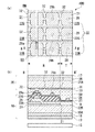
次に、図3に基づいて本実施の形態の液晶表示装置100の画素構成について説明する。図3(a)は、液晶表示装置100の画素構成、特に画素電極31の平面構成を示す模式図、図3(b)は図3(a)のA−A’断面を示す模式図である。本実施の形態の液晶表示装置100は、図2に示したようにデータ線9及び走査線13等にて囲まれた領域の内側に画素電極31を備えてなるドット領域を有している。このドット領域内には、図3(a)に示すように一のドット領域に対応して3原色のうちの一の着色層が配設され、3つのドット領域(D1,D2,D3)で各着色層22B(青色),22G(緑色),22R(赤色)を含む画素を形成している。
【0023】
一方、図3(b)に示すように、本実施の形態の液晶表示装置100は、上基板(素子基板)25とこれに対向配置された下基板(対向基板)10との間に初期配向状態が垂直配向をとる液晶、すなわち誘電異方性が負の液晶材料からなる液晶層50が挟持されている。
【0024】
下基板10は、石英、ガラス等の透光性材料からなる基板本体10Aの表面にアルミニウム、銀等の反射率の高い金属膜からなる反射膜20が所定パターンにて形成され、具体的には反射表示領域Rに選択的に形成されている。なお、表面に凹凸形状を備えた絶縁膜を基板本体10A上に形成し、該絶縁膜を介して反射膜20を形成することにより、該反射膜20の表面に散乱用の凹凸形状を付与することも可能である。ここで、反射膜20の形成領域が反射表示領域Rとなり、反射膜20の非形成領域、すなわち反射膜20の開口部21内が透過表示領域Tとなる。このように本実施の形態の液晶表示装置は、垂直配向型の液晶層50を備える垂直配向型液晶表示装置であって、反射表示及び透過表示を可能にした半透過反射型の液晶表示装置である。
【0025】
反射表示領域Rに選択的に形成された反射膜20上、及び透過表示領域T内に位置する基板本体10A上には、これら反射表示領域R及び透過表示領域Tに跨って形成されるカラーフィルタ22(22R,22G,22B)が設けられている。カラーフィルタ22は赤色、緑色、青色の各色着色層22R,22G,22Bを備えてなり、各色着色層22R,22G,22Bが各ドット領域D1,D2、D3を形成している(図3(a)参照)。
【0026】
ここで、本実施形態では、各ドット領域D1,D2、D3の境界領域に形成されるブラックマトリクスBMが従来汎用されている金属クロムではなく、各色の着色層22R,22G,22Bの積層体にて構成されている。具体的には、反射表示領域Rに隣接するドット間領域において、各色の着色層22R,22G,22Bが平面的に重なって形成されており、その積層体により黒が表示される構成となっている。なお、このように各着色層を積層した結果、当該ドット間領域において、該積層分だけカラーフィルタ22の層厚が厚膜に形成されることとなる。
【0027】
さらに、このカラーフィルタ22上には、反射表示領域Rに対応する位置に液晶層厚調整層たる絶縁膜26が略選択的に形成されている。すなわち、カラーフィルタ22を介して反射膜20の上方に位置するように選択的に絶縁膜26が形成され、該絶縁膜26の形成に伴って液晶層50の層厚を反射表示領域Rと透過表示領域Tとで異ならしめている。絶縁膜26は例えば膜厚が0.5〜2.5μm程度のアクリル樹脂等の有機膜からなり、反射表示領域Rと透過表示領域Tとの境界付近において、自身の層厚が連続的に変化するべく傾斜面を備えている。絶縁膜26が存在しない部分の液晶層50の厚みが1〜5μm程度とされ、反射表示領域Rにおける液晶層50の厚みは透過表示領域Tにおける液晶層50の厚みの約半分とされている。
【0028】
このように絶縁膜26は、自身の膜厚によって反射表示領域Rと透過表示領域Tとの液晶層50の層厚を異ならせる液晶層厚調整層(液晶層厚制御層)として機能するものである。また、本実施の形態の場合、絶縁膜26の上部の平坦面の縁と反射膜20(反射表示領域)の縁とが略一致しており、絶縁膜26の傾斜領域の一部又は全部が透過表示領域Tに含まれることになる。
【0029】
次に、絶縁膜26の表面を含む下基板10の表面には、インジウム錫酸化物(Indium Tin Oxide, 以下、ITOと略記する)からなる共通電極9が形成され、共通電極9上には突起28,29aが形成されている。なお、突起28は透過表示領域Tに、突起29aはドット間領域に配設されている。
【0030】
上述したようにカラーフィルタ22の各着色層22R,22G,22Bが重なって形成された領域においては、該積層分だけ絶縁膜26が突出して構成されており、さらにその絶縁膜26の突出部分には液晶層50側に突出してなる突起29aが形成されている。この突起29aは、透過表示領域Tに形成された突起28と同一材料にて構成されており、さらに該突起28と略同一の高さにて構成され、上基板25の液晶層挟持面に接する形にて液晶層厚(セルギャップ)を規制している。
【0031】
次に、共通電極9上にはポリイミド等からなる配向膜27が形成されている。配向膜27は液晶分子を膜面に対して垂直に配向させる垂直配向膜として機能するものであって、ラビングなどの配向処理は施されていない。なお、図3において共通電極9は、紙面垂直方向に延びる形のストライプ状に形成されており、該紙面垂直方向に並んで形成されたドット領域の各々に共通の電極として構成されている。また、本実施の形態では、反射膜20と共通電極9とを別個に設けて積層したが、反射表示領域Rにおいては金属膜からなる反射膜を共通電極の一部として用いることも可能である。
【0032】
一方、上基板25側においては、ガラスや石英等の透光性材料からなる基板本体25A上(基板本体25Aの液晶層側)に、ITO等の透明導電膜からなるマトリクス状の画素電極31と、ポリイミド等からなる下基板10と同様の垂直配向処理された配向膜33とが形成されている。なお、画素電極31には、該電極の一部を部分的に切り欠いた形状のスリット32が形成されている。
【0033】
次に、下基板10の外面側(液晶層50を挟持する面とは異なる側)には位相差板18及び偏光板19が、上基板25の外面側にも位相差板16及び偏光板17が形成されており、基板内面側(液晶層50側)に円偏光を入射可能に構成されており、これら位相差板18及び偏光板19、位相差板16及び偏光板17が、それぞれ円偏光板を構成している。偏光板17(19)は、所定方向の偏光軸を備えた直線偏光のみを透過させる構成とされ、位相差板16(18)としてはλ/4位相差板が採用されている。なお、下基板10に形成された偏光板19の外側には透過表示用の光源たるバックライト15が設けられている。
【0034】
ここで、本実施の形態の液晶表示装置100においては、液晶層50の液晶分子を配向規制するために、つまり初期状態において垂直配向にある液晶分子について、電極間に電圧を印加した際の傾倒方向を規制する手段として、電極の内面側(液晶層側)に誘電体からなる突起を形成している。図3の例においては、下基板10側に形成された共通電極9の内面側(液晶層側)であって、透過表示領域Tに位置する部分に突起28が形成されている。
【0035】
突起28は、基板内面(電極主面)から液晶層50の内部に突出する形にて円錐状若しくは多角錘状に構成され、その突出高さは約L1=1.0μm程度とされている。また、突起28は、基板内面(電極主面)に対して所定の角度で傾斜する傾斜面(緩やかに湾曲した形状を含む)を少なくとも備え、該傾斜面に沿って液晶分子LCの傾倒方向を規制するものとされている。
【0036】
一方、上基板25の内面側に形成された画素電極31には、該電極の一部を部分的に切り欠いた形状のスリット32が形成されている。該スリット32を設けたことにより、該スリット形成領域において各電極9,31間に斜め電界が生じ、該斜め電界に応じて、初期状態で垂直配向した液晶分子の電圧印加に基づく傾倒方向が規制されることとなる。なお、図3(a)に示すように、画素電極31に形成されたスリット32は、共通電極9に形成された突起28を取り囲む形にて構成されており、その結果、突起28の周りに沿って液晶分子LCの傾倒方向を放射状に規制することが可能となる。
【0037】
以上のような構成の液晶表示装置100によれば、以下のような効果を発現することができるようになる。
つまり、一般的には、ラビング処理を施さない垂直配向膜上に配向した負の誘電異方性を有する液晶分子に電圧を印加すると、液晶の倒れる方向に規制がないので無秩序な方向に倒れ、配向不良が生じることとなる。しかしながら、本実施の形態では、共通電極9の内面側に突起28を形成し、さらにその突起28を平面的に観て取り囲む形にて画素電極31にスリット32を形成したため、突起28の傾斜面による配向規制、及び/又はスリット32に基づく斜め電界による配向規制が生じ、初期状態で垂直配向した液晶分子の、電圧印加により倒れる方向が規制されることとなる。その結果、液晶配向不良に基づくディスクリネーションの発生が抑制されるため、ディスクリネーションの発生に伴う残像や斜め方向から観察したときのざらざらとしたしみ状のムラ等が発生し難い高品質な表示が得られる。
【0038】
また、カラーフィルタ22を構成する各着色層22R,22G,22Bの積層体によりドット間のブラックマトリクスを構成するものとしているため、別途金属クロムを用いることなくブラックマトリクスBMを形成することができるため、製造効率が向上し、コスト削減を可能とするとともに、金属クロム等の廃棄による環境破壊の問題も回避することが可能となり得る。
【0039】
さらに、本実施形態の液晶表示装置100では、反射表示領域Rに絶縁膜26を設けたことによって反射表示領域Rの液晶層50の厚みを透過表示領域Tの液晶層50の厚みの略半分と小さくすることができるので、反射表示に寄与するリタデーションと透過表示に寄与するリタデーションを略等しくすることができ、これによりコントラストの向上が図られている。
【0040】
そして、この絶縁膜26上には、着色層22R,22G,22Bが積層された領域に対応して、液晶層厚(セルギャップ)を規制するための突起29aが形成されているため、従来のようなスペーサーを別途用いることなく液晶層厚を規制することが可能で、製造効率が向上し、コスト削減を実現することが可能となる。
【0041】
また、ここでは重ねた着色層22R,22G,22B上に突起29aを直接形成することなく、絶縁膜26を介して形成しているため、該突起29aを容易に形成することが可能となっている。つまり、突起29aはセルギャップを規制する手段であるため、配設する際には高い精度が要求されるが、例えば重ねた着色層22R,22G,22B上に直接形成する場合には、その形成面が極めて小さい面積であるため配設が困難となる場合があるものの、本実施形態のように絶縁膜26を介して配設することで、その配設面積が大きくなり、配設に係る位置精度が向上する上、配設後の基板に対する突起29aの密着性も向上する等の効果が得られることとなる。その結果、設計通りの液晶層厚(セルギャップ)を容易に得ることができ、該液晶層厚(セルギャップ)の均一な信頼性の高い液晶表示装置を提供することが可能となる。
【0042】
次に、上記第1の実施の形態の液晶表示装置100について、その一製造工程を特に図3(b)を参照しつつ説明する。液晶表示装置100の製造工程の概略は、下基板10を製造する工程と、上基板25を製造する工程と、下基板10と上基板25とを液晶材料を介して貼り合せる工程とを含んでなるものである。以下、これら各工程の詳細について説明する。
【0043】
(下基板10の製造工程)
まず、基板本体10Aに相当する基材上に、Al等の金属材料を主体とする反射膜20を所定パターンにて形成(反射表示領域Rに相当する領域に形成)し、続いて反射膜20を備えた基板本体10A上の略全面に、R,G,Bの各色の着色層を含むカラーフィルタ22を形成する。なお、このカラーフィルタ22を形成する工程においては、各着色層22R,22G,22Bをドット間領域において平面的に重ねて形成するものとされており、このようなパターン形成は、例えばフォトリソグラフィ法を用いて行うことができる。ここで、カラーフィルタ22において、各着色層22R,22G,22Bを重ねて形成した領域には、該着色層の積層に基づく凸状部が形成されることとなる。
【0044】
カラーフィルタ22を形成した後、アクリル樹脂を主体として構成される液晶層厚調整層たる絶縁膜26を、反射膜20が形成された領域のカラーフィルタ22を覆う形にて略選択的に形成する。この場合、先に述べたカラーフィルタ22の凸状部に倣って、絶縁膜26にも同様の凸状部がドット間領域に形成されることとなる。
【0045】
その後、これら反射膜20、カラーフィルタ22、絶縁膜26等を備える基板本体10A上に、ITOを主体とするストライプ状の透明電極9を例えばスパッタまたは蒸着法にて形成する。なお、ストライプ状のパターンはマスク蒸着により形成する手法、エッチングにより加工する手法のいずれを採用しても良い。
【0046】
続いて、このように基板本体10A上に形成した透明電極9上に、反射膜20の非形成領域、並びにドット間領域にそれぞれ誘電体からなる突起28、並びに突起29aを形成する。なお、突起29aは、特に上記絶縁膜26の凸状部に形成するものとしており、各突起28,29aはそれぞれ同一の高さにて形成するものとしている。
【0047】
以上のような方法により形成した突起28,29aを含む透明電極9上の略全面に、ポリイミドからなる垂直配向性の配向膜27を形成する。なお、該配向膜27にはラビングなどの配向処理は施さないものとする。
【0048】
一方、基板本体10Aの透明電極9等を形成した面とは反対側の面には、1/4波長板からなる位相差板18及び偏光板19を形成し、下基板10を得る。
【0049】
(上基板25の製造工程)
まず、基板本体25Aに相当する基材上に、ITOを主体とするマトリクス状の透明電極31を例えばスパッタまたは蒸着法にて形成する。なお、マトリクス状のパターンはマスク蒸着により形成する手法、エッチングにより加工する手法のいずれを採用しても良く、このマトリクス状のパターニングと同時にスリット32を形成するものとしている。続いて、このように基板本体25A上に形成した透明電極31上の略全面に、ポリイミドからなる垂直配向性の配向膜33を形成する。なお、該配向膜33にはラビングなどの配向処理は施さないものとする。
【0050】
一方、基板本体25Aの透明電極31等を形成した面とは反対側の面には、1/4波長板からなる位相差板16及び偏光板17を形成し、上基板25を得る。
【0051】
(基板貼合せ工程)
上記の方法により得られた上基板25と下基板10とを、液晶注入口を形成した紫外線硬化性樹脂等からなるシール材を介して真空中にて貼り合わせる。そして、その貼り合わせた基板に対して、液晶注入口から液晶材料を真空注入法により注入する。注入後、封止材にて液晶注入口を封止し、本実施形態の液晶表示装置100を得る。なお、本実施形態では、液晶材料として誘電異方性が負の液晶材料を用いている。
【0052】
以上、第1の実施の形態の液晶表示装置について示したが、例えば図6のような構成を付加することもできる。つまり、上記実施の形態では透過表示領域Tのみに突起28を形成しているが、図6に示すように反射表示領域Rに対しても、液晶分子の配向方向を規制するための突起29bを形成することができる。該反射表示領域Rに形成した突起29bは、ドット間領域の突起29aと略同一の高さにて形成することが好ましく、この場合、突起29bが対向する基板の内面に接してしまう不具合を解消でき、その結果、液晶分子の配向規制を良好に行うことが可能となる。また、透過表示領域Tの突起28と、反射表示領域Rの突起29bについては、透過表示領域Tの突起28の突出高さが反射表示領域Rの突起29bよりも相対的に大きく構成されたものとすることもできる。マルチギャップ構造の採用により透過表示領域Tの液晶層厚が相対的に大きく形成されているため、透過表示領域Tにおいては一層大きな配向規制力が必要であり、上記のように突出高さを設計するのが好ましい。
【0053】
[第2の実施の形態]
次に、第2の実施の形態の液晶表示装置について、図面を参照しつつ説明する。図4は、第2の実施の形態の液晶表示装置200について、その平面構造(a)及び断面構造(b)を示す模式図であって、第1の実施の形態の図3に相当する図面である。本第2の実施の形態の液晶表示装置200は、液晶配向規制を目的として形成した突起の形状が主として異なる以外は、図3に示した液晶表示装置100及び図6に示した液晶表示装置400と基本構造は略同様であり、したがって図3及び図6に付した符号と同一符号のものについては、特に記述がない限り同一の構成部材として説明を省略するものとする。
【0054】
図4に示すように、本実施形態の液晶表示装置200において、表示領域であるドット領域に形成する液晶配向規制用の突起28,29bをライン状に形成した。つまり、第1の実施の形態では、図3に示すように円錐状ないし多角錘状の突起にて形成したが、本実施の形態のようにドット内で一方向に延びるライン状突起として構成した場合、液晶分子の配向規制を一層良好に行うことが可能となる。
【0055】
[第3の実施の形態]
次に、第3の実施の形態の液晶表示装置について、図面を参照しつつ説明する。図5は、第3の実施の形態の液晶表示装置300について、その平面構造(a)及び断面構造(b)を示す模式図であって、第2の実施の形態の図4に相当する図面である。本第3の実施の形態の液晶表示装置300は、第2の実施の形態に比して、カラーフィルタ22が上基板25側に形成されている以外は、図4に示した液晶表示装置200と基本構造は略同様であり、したがって図4に付した符号と同一符号のものについては、同一の構成部材として説明を省略するものとする。
【0056】
第3の実施の形態の液晶表示装置300は、スイッチング素子として薄膜トランジスタ(TFT)を用いたアクティブマトリクス型の半透過反射型液晶表示装置の例であって、下基板(素子基板)10とこれに対向配置された上基板(対向基板)25との間に初期配向状態が垂直配向をとる液晶、すなわち誘電異方性が負の液晶材料からなる液晶層50が挟持されている。
【0057】
下基板10は、基板本体10Aの表面にアルミニウム、銀等の反射率の高い金属膜からなる反射膜20が所定パターンにて、具体的には反射表示領域Rに選択的に形成されている。さらに、反射膜20の形成されていない領域、すなわち透過表示領域Tには所定パターンの透明電極9aが形成され、これら反射膜20及び透明電極9aが一対になってマトリクス状に形成された画素電極を構成している。なお、画素電極には、該電極を部分的に切り欠いたスリット9b、20bが形成されており、該スリット9b、20bにおいて斜め電界が生じるものなっている。また、画素電極上には垂直配向性を有する配向膜27が形成されている。
【0058】
一方、上基板25は、基板本体25Aの表面に各色の着色層22R,22G,22Bを重ねて形成された領域を含むカラーフィルタ22が配設され、該カラーフィルタ22上には、液晶層厚調整層たる絶縁膜26と、全面ベタ状に形成された共通電極31aとが配設されている。また、共通電極31a上には、突起28,29b,29aが形成されており、それぞれ透過表示領域、反射表示領域、ドット間領域に位置してなるものである。これら突起28,29a,29bの構成については、上記第2の実施の形態と同様のものである。
【0059】
このように、本実施形態においても、画素電極の間に位置するカラーフィルタ22のドット間領域には、各着色層22R,22G,22Bが積層してなるブラックマトリクスBMが形成されている。具体的には、反射表示領域Rに隣接するドット間領域において、各色の着色層22R,22G,22Bが平面的に重なって形成されており、その積層体により黒が表示される構成となっている。なお、このように各着色層を積層した結果、当該ドット間領域において、該積層分だけカラーフィルタ22の層厚が厚膜に形成されることとなる。
【0060】
以上のように、各着色層22R,22G,22Bを積層してブラックマトリクスを構成したカラーフィルタ22を上基板25側に含む液晶表示装置300によっても、第1の実施の形態の液晶表示装置100及び第2の実施の形態の液晶表示装置200が具備する幾つかの効果を奏することが可能となる。
【0061】
[電子機器]
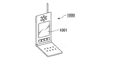
次に、本発明の上記実施の形態の液晶表示装置を備えた電子機器の具体例について説明する。
図7は、携帯電話の一例を示した斜視図である。図7において、符号1000は携帯電話本体を示し、符号1001は上記液晶表示装置を用いた表示部を示している。このような電子機器は、上記実施の形態の液晶表示装置を用いた表示部を備えているので、使用環境によらずに明るく、コントラストが高く、広視野角の液晶表示部を備えた電子機器を実現することができる。
【0062】
以上、本発明の実施の形態について、その一例を説明したが、本発明の技術範囲はこれらに限定されるものではなく、本発明の趣旨を逸脱しない範囲において種々の変更を加えることが可能である。例えば上記実施の形態では位相差板を単板で構成したが、この代わりに、1/2波長板と1/4波長板との積層体として構成してもよい。この積層体は広帯域円偏光板として機能し、黒表示をより無彩色化にすることができる。また、本実施の形態で形成した突起の形状、電極スリットの形状についても、上記実施の形態の構成に限られるものではなく、少なくとも垂直配向した液晶分子の傾倒方向を規制するための構成を具備していれば良い。
【図面の簡単な説明】
【図1】第1実施形態の液晶表示装置の等価回路図。
【図2】図1の液晶表示装置の電極構成を平面的に示す説明図。
【図3】図1の液晶表示装置について要部を拡大して示す平面模式図及び断面模式図。
【図4】第2実施形態の液晶表示装置について要部を拡大して示す平面模式図及び断面模式図。
【図5】第3実施形態の液晶表示装置について要部を拡大して示す平面模式図及び断面模式図。
【図6】第1実施形態の液晶表示装置の変形例について要部を拡大して示す平面模式図及び断面模式図。
【図7】本発明の電子機器の一例を示す斜視図。
【符号の説明】
9…共通電極、20…反射膜、26…絶縁膜(液晶層厚調整層)、28,29a,29b…突起、31…画素電極、50…液晶層、R…反射表示領域、T…透過表示領域[0001]
TECHNICAL FIELD OF THE INVENTION
The present invention relates to a liquid crystal display device and an electronic apparatus, and more particularly to a technique for obtaining a display with a wider viewing angle in a liquid crystal display device using a vertically aligned liquid crystal.
[0002]
[Prior art]
2. Description of the Related Art As a liquid crystal display device, a transflective liquid crystal display device having both a reflection mode and a transmission mode is known. As such a transflective liquid crystal display device, a liquid crystal layer is sandwiched between an upper substrate and a lower substrate, and a reflection film in which a light transmission window is formed in a metal film such as aluminum is disposed below. There has been proposed a device provided on the inner surface of a substrate and using this reflection film as a transflective plate. In this case, in the reflection mode, external light incident from the upper substrate side passes through the liquid crystal layer, is reflected by the reflection film on the inner surface of the lower substrate, passes through the liquid crystal layer again, and is emitted from the upper substrate side, contributing to display. I do. On the other hand, in the transmission mode, light from the backlight incident from the lower substrate side passes through the liquid crystal layer from the window of the reflection film, and then exits from the upper substrate side to contribute to display. Therefore, of the reflective film forming region, the region where the window is formed is the transmissive display region, and the other region is the reflective display region.
[0003]
However, the conventional transflective liquid crystal device has a problem that the viewing angle in transmissive display is narrow. This is because a transflective plate is provided on the inner surface of the liquid crystal cell so that parallax does not occur, and there is a restriction that reflective display must be performed with only one polarizing plate provided on the viewer side. This is because the degree of freedom in design is small. In order to solve this problem, Jisaki et al. Proposed a new liquid crystal display device using a vertically aligned liquid crystal in Non-Patent Document 1 below. The features are the following three.
(1) A "VA (Vertical Alignment) mode" in which a liquid crystal having a negative dielectric anisotropy is vertically aligned with a substrate and is tilted by applying a voltage.
(2) A multi-gap structure in which the liquid crystal layer thickness (cell gap) of the transmissive display region and the reflective display region is different (for this point, see, for example, Patent Document 1).
(3) The transmissive display area is a regular octagon, and a projection is provided at the center of the transmissive display area on the opposing substrate so that the liquid crystal falls in eight directions in this area. That is, an "alignment division structure" is adopted.
[0004]
[Patent Document 1]
JP-A-11-242226
[Patent Document 2]
JP-A-2002-350853
[Non-patent document 1]
"Development of transflective LCD for high contrast and wide viewing angle by using homeotropic alignment", M.D. Jisaki et al. , Asia Display / IDW'01, p. 133-136 (2001)
[0005]
[Problems to be solved by the invention]
Providing the transflective liquid crystal display device with a multi-gap structure as disclosed in Japanese Patent Application Laid-Open No. H10-15095 is effective in making the electro-optical characteristics (transmittance-voltage characteristics, reflectance-voltage characteristics) of the transmissive display region and the reflective display region uniform. It is very effective. This is because light passes through the liquid crystal layer only once in the transmissive display area, but passes through the liquid crystal layer twice in the reflective display area.
[0006]
However, when adopting such a multi-gap structure and trying to control the direction in which the liquid crystal falls using the projections as described above, for example, when arranging a spacer for regulating the thickness of the liquid crystal layer, May float in the transmissive display area where the thickness of the liquid crystal layer is large, or the design may need to be performed while considering the height of the protrusion and the size of the spacer, which may be complicated. In other words, in a liquid crystal display device in which projections for restricting the direction in which the liquid crystal falls are added to the multi-gap structure, it takes time to design the liquid crystal layer thickness, and in particular, the liquid crystal layer thickness greatly affects display characteristics. If an error occurs in the design, it may cause a defect.
[0007]
The present invention has been made to solve the above-described problems, and in a transflective liquid crystal display device using a vertically aligned liquid crystal, a display with a wide viewing angle is possible, and a liquid crystal layer is provided. It is an object of the present invention to provide a liquid crystal display device having a more preferable structure for regulating the thickness (substrate interval, so-called cell gap). It is another object of the present invention to provide a transflective liquid crystal display device using a vertical alignment type liquid crystal, which enhances manufacturing efficiency by simplifying the configuration and provides a highly reliable liquid crystal display device with less occurrence of defects. It is another object of the present invention to provide a highly reliable electronic device including the liquid crystal display device.
[0008]
[Means for Solving the Problems]
In order to achieve the above object, a liquid crystal display device of the present invention includes a liquid crystal display in which a liquid crystal layer is sandwiched between a pair of substrates, and a transmissive display area and a reflective display area are provided in one dot area. The liquid crystal layer is composed of a liquid crystal having a negative dielectric anisotropy in which an initial alignment state is vertical alignment, and a color filter is provided between at least one of the pair of substrates and the liquid crystal layer. A color filter layer comprising a plurality of coloring layers, wherein the plurality of coloring layers are formed so as to overlap in a plane in the inter-dot region, and the liquid crystal layer thickness of the reflective display region is A liquid crystal layer thickness adjusting layer for reducing the thickness of the liquid crystal layer in the transmissive display region is provided so as to cover at least a region of the color filter layer where the colored layers overlap, and further includes a liquid crystal layer thickness adjusting layer. Transparent inside While a pole is provided, the dot region is provided with a first convex portion projecting from the inner surface of the transparent electrode to the inside of the liquid crystal layer. On the liquid crystal layer thickness adjusting layer in a region where the coloring layer overlaps, a second convex portion protruding from the inner surface of the transparent electrode to the inside of the liquid crystal layer is provided.
[0009]
The liquid crystal display device of the present invention combines a vertical alignment mode liquid crystal with a transflective liquid crystal display device, and further includes a liquid crystal layer thickness adjustment layer for making retardation in a reflective display region and retardation in a transmissive display region substantially equal. This is an addition (that is, an addition of a multi-gap structure), and has a configuration for suitably controlling the orientation direction of liquid crystal molecules. Further, a black matrix is formed by overlapping a colored layer in an inter-dot region, and a liquid crystal layer thickness (substrate interval: hereinafter also referred to as a cell gap) is formed by the protrusions formed in the black matrix shape, whereby a liquid crystal display device is formed. And the cell gap can be further secured as designed.
[0010]
That is, in the liquid crystal display device of the vertical alignment mode, the liquid crystal molecules standing vertically to the substrate surface in the initial alignment state are tilted by applying an electric field, but if no measures are taken (pretilt is applied. If it is not, the direction in which the liquid crystal molecules fall cannot be controlled, and disorder in the alignment (disclination) occurs, causing display defects such as light leakage and degrading the display quality. Therefore, in adopting the vertical alignment mode, control of the alignment direction of liquid crystal molecules when an electric field is applied is an important factor. Therefore, in the liquid crystal display device of the present invention, it is possible to form the first convex portion in the dot region (that is, the transmissive display region and / or the reflective display region) and regulate the orientation direction of the liquid crystal molecules in the region. And Due to such alignment regulation, the liquid crystal molecules exhibit vertical alignment in the initial state and have a pretilt according to the shape of the convex portion. As a result, when the vertically-aligned liquid crystal molecules fall, alignment disorder (disclination) is unlikely to occur, and display defects such as light leakage can be avoided. In addition, a liquid crystal display device having a wide viewing angle can be provided.
[0011]
Further, since the liquid crystal display device of the present invention employs a multi-gap structure, the thickness of the liquid crystal layer in the transmissive display area is configured to be larger than the thickness of the liquid crystal layer in the reflective display area. It is possible to make the electro-optical characteristics (transmittance-voltage characteristics, reflectance-voltage characteristics) of the reflective display area uniform.
[0012]
Furthermore, a plurality of coloring layers (for example, a plurality of coloring layers corresponding to three primary colors of light) are formed so as to overlap in a plane between dots in a region between at least one of the pair of substrates and the liquid crystal layer. A color filter layer having the structure described above is provided, and the liquid crystal layer thickness adjusting layer is provided so as to cover at least a region where the colored layers of the color filter layer overlap, while the colored layer is an inter-dot region. Are arranged on the liquid crystal layer thickness adjusting layer in the region where the liquid crystal layer overlaps, the following effects can be obtained because the second convex portions projecting from the inner surface of the transparent electrode into the liquid crystal layer are provided. .
First, it was possible to display black by forming the coloring layers in an overlapping manner, and it was possible to use the overlapping coloring layers as a black matrix in a region between dots. Therefore, there is no need to separately form a black matrix, so that the configuration of the liquid crystal display device is simplified and the manufacturing efficiency is improved.
Further, in the case of the above configuration, the liquid crystal layer thickness adjusting layer is formed so as to be thicker in the overlapping region of the colored layer by the thickness of the colored layer that is formed by overlapping the colored layer. Since the second convex portion is formed on the thick portion, the second convex portion is formed at the highest position on the substrate (that is, formed most protruding in the substrate plane). As a result, The second convex portion can be used as a liquid crystal layer thickness regulating means for maintaining the cell gap at a predetermined thickness.
Further, in particular, in the present invention, the second convex portion is formed via the liquid crystal layer thickness adjusting layer without directly forming the second convex portion on the stacked colored layers. Can be easily formed. In other words, since the second convex portion is a means for regulating the cell gap, high accuracy is required when the second convex portion is disposed. For example, when the second convex portion is formed directly on the stacked colored layers, Although the arrangement may be difficult due to the extremely small area, the arrangement area is increased by disposing via the liquid crystal layer thickness adjustment layer as described above, and the positional accuracy related to the arrangement is improved. In addition, effects such as improvement in the adhesion of the second convex portion after the arrangement can be obtained. As a result, a cell gap as designed can be easily obtained, and a highly reliable liquid crystal display device having a uniform cell gap can be provided. In addition, since it is not necessary to separately provide a spacer or the like, the configuration is simple, and problems such as floating of the spacer in a transmissive display region having a relatively thick liquid crystal layer do not occur.
[0013]
In the liquid crystal display device according to the aspect of the invention, the first convex portion is provided as an alignment control unit for controlling the alignment of the liquid crystal, and is inclined at a predetermined angle with respect to a surface of the substrate that sandwiches a liquid crystal layer. It is possible to have an inclined surface, and by providing such an inclined surface, it is possible to regulate the tilt direction of the liquid crystal along the inclined surface. Here, in the liquid crystal display device of the present invention, since the visibility in the transmission mode is higher than that in the reflection mode, the first convex portion is formed at least in the transmission display region among the dot regions. It is good. In the present invention, for example, the inner surface side of the substrate means the liquid crystal layer side of the substrate, and the protrusion from the substrate surface means that the liquid crystal layer thickness adjustment layer is formed on the inner surface of the substrate, for example. In this case, it means that the convex portion protrudes from the inner surface of the liquid crystal layer thickness adjusting layer.
[0014]
Further, electrodes for driving the liquid crystal are provided on the liquid crystal layer side of the pair of substrates, respectively, and the first and second convex portions are provided on the liquid crystal layer side of at least one of the electrodes. In this case, an alignment film for vertically aligning the liquid crystal is formed on each convex portion and on the inner surface side of the electrode in the liquid crystal layer. Further, a circularly polarizing plate for entering circularly polarized light into the liquid crystal layer can be provided on a side of the pair of substrates different from the liquid crystal layer. As the circularly polarizing plate, a combination of a polarizing layer and a retardation layer can be used.
[0015]
Further, the liquid crystal display device of the present invention includes an upper substrate and a lower substrate as a pair of substrates, and a backlight for transmissive display is provided on a side of the lower substrate opposite to the liquid crystal layer, and a liquid crystal layer of the lower substrate is provided. On the side, a reflective layer selectively formed in the reflective display area can be provided. In this case, light from the backlight incident from the lower substrate side can be used for transmission display, and external light such as illumination and sunlight incident from the upper substrate side can be reflected by the reflection layer to be used for reflection display. become.
[0016]
The second convex portion is preferably formed by the same process as the first convex portion formed in the dot region for the purpose of improving manufacturing efficiency. In this case, the first convex portion and the second convex portion are formed. The shape part is made of the same material.
In addition, the second convex portion may be configured to have substantially the same height as the first convex portion formed in the dot region. In this case, the second convex portion can be suitably used as the liquid crystal layer thickness regulating means without considering the height relationship with the first convex portion, while the first convex portion formed in the dot region is not used. Since the projections are formed with substantially the same height as the second projections, it is possible to prevent or suppress the first projections from contacting the opposing substrate, and to sufficiently control the alignment of the liquid crystal. Can be expressed.
[0017]
Next, an electronic apparatus according to the present invention includes the above-described liquid crystal display device. According to such an electronic device, it is possible to provide an electronic device including a display unit capable of performing both the transmission mode and the reflection mode and providing a display with a wide viewing angle in each display mode. .
[0018]
BEST MODE FOR CARRYING OUT THE INVENTION
[First Embodiment]
Hereinafter, embodiments according to the present invention will be described with reference to the drawings. In each of the drawings, the scale of each layer and each member is different so that each layer and each member have a size that can be recognized in the drawings.
[0019]
The liquid crystal display device of the present embodiment described below is an example of an active matrix type liquid crystal display device using a thin film diode (hereinafter abbreviated as TFD) as a switching element. This is a transflective liquid crystal display device that enables display.
FIG. 1 shows an equivalent circuit of the liquid
[0020]
Next, a planar structure of an electrode provided in the liquid crystal display device of the present embodiment will be described with reference to FIG. As shown in FIG. 2, in the liquid crystal display device of the present embodiment, a
[0021]
Here, the
[0022]
Next, a pixel configuration of the liquid
[0023]
On the other hand, as shown in FIG. 3B, the liquid
[0024]
In the
[0025]
On the
[0026]
Here, in the present embodiment, the black matrix BM formed in the boundary area between the dot areas D1, D2, and D3 is not a metal chromium conventionally used in general, but a laminate of the
[0027]
Further, on the
[0028]
As described above, the insulating
[0029]
Next, a
[0030]
As described above, in the region where the
[0031]
Next, an
[0032]
On the other hand, on the
[0033]
Next, the
[0034]
Here, in the liquid
[0035]
The
[0036]
On the other hand, the
[0037]
According to the liquid
In other words, in general, when a voltage is applied to liquid crystal molecules having negative dielectric anisotropy aligned on a vertical alignment film that is not subjected to rubbing, the liquid crystal falls in a disordered direction because there is no regulation on the direction in which the liquid crystal falls. Poor alignment will occur. However, in the present embodiment, the
[0038]
In addition, since a black matrix between dots is formed by a stacked body of the coloring layers 22R, 22G, and 22B forming the
[0039]
Furthermore, in the liquid
[0040]
On the insulating
[0041]
In addition, since the
[0042]
Next, one manufacturing process of the liquid
[0043]
(Manufacturing process of lower substrate 10)
First, a
[0044]
After the
[0045]
After that, the stripe-shaped
[0046]
Subsequently, on the
[0047]
A
[0048]
On the other hand, on the surface of the
[0049]
(Manufacturing process of upper substrate 25)
First, a matrix-shaped
[0050]
On the other hand, on the surface of the substrate
[0051]
(Substrate bonding process)
The
[0052]
The liquid crystal display device according to the first embodiment has been described above. However, for example, a configuration as shown in FIG. 6 can be added. That is, in the above embodiment, the
[0053]
[Second embodiment]
Next, a liquid crystal display device according to a second embodiment will be described with reference to the drawings. FIG. 4 is a schematic diagram showing a planar structure (a) and a cross-sectional structure (b) of the liquid
[0054]
As shown in FIG. 4, in the liquid
[0055]
[Third Embodiment]
Next, a liquid crystal display device according to a third embodiment will be described with reference to the drawings. FIG. 5 is a schematic view showing a planar structure (a) and a cross-sectional structure (b) of the liquid
[0056]
The liquid
[0057]
In the
[0058]
On the other hand, the
[0059]
As described above, also in the present embodiment, the black matrix BM formed by laminating the coloring layers 22R, 22G, and 22B is formed in the inter-dot region of the
[0060]
As described above, the liquid
[0061]
[Electronics]
Next, a specific example of an electronic apparatus including the liquid crystal display device according to the above embodiment of the present invention will be described.
FIG. 7 is a perspective view showing an example of a mobile phone. In FIG. 7,
[0062]
As described above, an example of the embodiment of the present invention has been described, but the technical scope of the present invention is not limited thereto, and various changes can be made without departing from the spirit of the present invention. is there. For example, in the above embodiment, the retardation plate is constituted by a single plate, but may be constituted by a laminate of a half-wave plate and a quarter-wave plate instead. This laminate functions as a broadband circularly polarizing plate, and can make the black display more achromatic. Further, the shape of the projection and the shape of the electrode slit formed in this embodiment are not limited to the structure of the above embodiment, and at least a structure for regulating the tilt direction of the vertically aligned liquid crystal molecules is provided. Just do it.
[Brief description of the drawings]
FIG. 1 is an equivalent circuit diagram of a liquid crystal display device according to a first embodiment.
FIG. 2 is an explanatory diagram showing a plan view of an electrode configuration of the liquid crystal display device of FIG. 1;
FIGS. 3A and 3B are a schematic plan view and a schematic cross-sectional view illustrating a main part of the liquid crystal display device in FIG. 1 in an enlarged manner.
4A and 4B are a schematic plan view and a schematic cross-sectional view illustrating a main part of a liquid crystal display device according to a second embodiment in an enlarged manner.
5A and 5B are a schematic plan view and a schematic cross-sectional view illustrating a main part of a liquid crystal display device according to a third embodiment in an enlarged manner.
6A and 6B are a schematic plan view and a schematic cross-sectional view showing a main part of a modification of the liquid crystal display device of the first embodiment in an enlarged manner.
FIG. 7 is a perspective view illustrating an example of an electronic apparatus of the invention.
[Explanation of symbols]
9: Common electrode, 20: Reflective film, 26: Insulating film (liquid crystal layer thickness adjusting layer), 28, 29a, 29b: Projection, 31: Pixel electrode, 50: Liquid crystal layer, R: Reflective display area, T: Transmissive display region
Claims (9)
前記液晶層は、初期配向状態が垂直配向を呈する誘電異方性が負の液晶からなり、
前記一対の基板のうちの少なくとも一方の基板と前記液晶層との間にカラーフィルタ層が設けられ、該カラーフィルタ層は複数の着色層を備えてなり、該複数の着色層がドット間領域において平面的に重なって形成されてなるとともに、
前記反射表示領域の液晶層厚を前記透過表示領域の液晶層厚よりも小さくするための液晶層厚調整層が、前記カラーフィルタ層の前記着色層が重なった領域を少なくとも覆う形にて配設され、さらに該液晶層厚調整層の内面側には透明電極が配設されてなる一方、
前記ドット領域には、前記透明電極内面から前記液晶層内部に突出する第1凸状部が設けられ、さらに前記ドット間領域であって、前記カラーフィルタ層の前記着色層が重なった領域の前記液晶層厚調整層上には、同じく前記透明電極内面から前記液晶層内部に突出する第2凸状部が設けられていることを特徴とする液晶表示装置。A liquid crystal display device in which a liquid crystal layer is sandwiched between a pair of substrates, and a transmissive display region and a reflective display region are provided in one dot region,
The liquid crystal layer is composed of a liquid crystal having a negative dielectric anisotropy in which an initial alignment state exhibits vertical alignment,
A color filter layer is provided between at least one of the pair of substrates and the liquid crystal layer, the color filter layer includes a plurality of coloring layers, and the plurality of coloring layers are in an inter-dot region. While being formed to overlap in a plane,
A liquid crystal layer thickness adjusting layer for making the liquid crystal layer thickness of the reflective display region smaller than the liquid crystal layer thickness of the transmissive display region is provided so as to cover at least the region of the color filter layer where the colored layers overlap. Further, while a transparent electrode is disposed on the inner surface side of the liquid crystal layer thickness adjustment layer,
In the dot region, a first convex portion protruding from the inner surface of the transparent electrode to the inside of the liquid crystal layer is provided, and furthermore, the inter-dot region, in which the colored layer of the color filter layer overlaps the A liquid crystal display device further comprising a second convex portion protruding from the inner surface of the transparent electrode into the liquid crystal layer on the liquid crystal layer thickness adjusting layer.
Priority Applications (1)
| Application Number | Priority Date | Filing Date | Title |
|---|---|---|---|
| JP2003162354A JP4432371B2 (en) | 2003-06-06 | 2003-06-06 | Liquid crystal display device and electronic device |
Applications Claiming Priority (1)
| Application Number | Priority Date | Filing Date | Title |
|---|---|---|---|
| JP2003162354A JP4432371B2 (en) | 2003-06-06 | 2003-06-06 | Liquid crystal display device and electronic device |
Publications (3)
| Publication Number | Publication Date |
|---|---|
| JP2004361824A true JP2004361824A (en) | 2004-12-24 |
| JP2004361824A5 JP2004361824A5 (en) | 2006-05-18 |
| JP4432371B2 JP4432371B2 (en) | 2010-03-17 |
Family
ID=34054527
Family Applications (1)
| Application Number | Title | Priority Date | Filing Date |
|---|---|---|---|
| JP2003162354A Expired - Fee Related JP4432371B2 (en) | 2003-06-06 | 2003-06-06 | Liquid crystal display device and electronic device |
Country Status (1)
| Country | Link |
|---|---|
| JP (1) | JP4432371B2 (en) |
Cited By (8)
| Publication number | Priority date | Publication date | Assignee | Title |
|---|---|---|---|---|
| JP2006201357A (en) * | 2005-01-19 | 2006-08-03 | Sharp Corp | Liquid crystal display |
| JP2006292940A (en) * | 2005-04-08 | 2006-10-26 | Sony Corp | Liquid crystal display device |
| JP2006330602A (en) * | 2005-05-30 | 2006-12-07 | Sharp Corp | Liquid crystal display device and its manufacturing method |
| KR100744393B1 (en) | 2006-04-06 | 2007-07-30 | 비오이 하이디스 테크놀로지 주식회사 | Transflective type lcd having wide viewing angle and method of manufacturing the same |
| KR100828858B1 (en) * | 2005-08-29 | 2008-05-09 | 가부시키가이샤 히타치 디스프레이즈 | Liquid Crystal Display Apparatus, and Information Terminal Having the Same |
| JP2011059725A (en) * | 2010-12-22 | 2011-03-24 | Sharp Corp | Liquid crystal display device |
| US8040471B2 (en) | 2008-07-01 | 2011-10-18 | Samsung Electronics Co., Ltd. | Liquid crystal display including color filters, and manufacturing method thereof |
| JP2014142643A (en) * | 2007-07-27 | 2014-08-07 | Semiconductor Energy Lab Co Ltd | Semiconductor device |
Families Citing this family (1)
| Publication number | Priority date | Publication date | Assignee | Title |
|---|---|---|---|---|
| JP7331614B2 (en) | 2019-10-16 | 2023-08-23 | 凸版印刷株式会社 | liquid crystal display |
-
2003
- 2003-06-06 JP JP2003162354A patent/JP4432371B2/en not_active Expired - Fee Related
Cited By (8)
| Publication number | Priority date | Publication date | Assignee | Title |
|---|---|---|---|---|
| JP2006201357A (en) * | 2005-01-19 | 2006-08-03 | Sharp Corp | Liquid crystal display |
| JP2006292940A (en) * | 2005-04-08 | 2006-10-26 | Sony Corp | Liquid crystal display device |
| JP2006330602A (en) * | 2005-05-30 | 2006-12-07 | Sharp Corp | Liquid crystal display device and its manufacturing method |
| KR100828858B1 (en) * | 2005-08-29 | 2008-05-09 | 가부시키가이샤 히타치 디스프레이즈 | Liquid Crystal Display Apparatus, and Information Terminal Having the Same |
| KR100744393B1 (en) | 2006-04-06 | 2007-07-30 | 비오이 하이디스 테크놀로지 주식회사 | Transflective type lcd having wide viewing angle and method of manufacturing the same |
| JP2014142643A (en) * | 2007-07-27 | 2014-08-07 | Semiconductor Energy Lab Co Ltd | Semiconductor device |
| US8040471B2 (en) | 2008-07-01 | 2011-10-18 | Samsung Electronics Co., Ltd. | Liquid crystal display including color filters, and manufacturing method thereof |
| JP2011059725A (en) * | 2010-12-22 | 2011-03-24 | Sharp Corp | Liquid crystal display device |
Also Published As
| Publication number | Publication date |
|---|---|
| JP4432371B2 (en) | 2010-03-17 |
Similar Documents
| Publication | Publication Date | Title |
|---|---|---|
| JP3778179B2 (en) | Liquid crystal display device, method for manufacturing liquid crystal display device, electronic device | |
| US7403246B2 (en) | Liquid crystal display device and electronic apparatus | |
| US7471363B2 (en) | Vertical alignment model LCD with larger dielectric protrusions in transmissive region than in reflection region | |
| US7259816B2 (en) | Liquid crystal display device and electronic apparatus | |
| JP2004333700A (en) | Liquid crystal display device and electronic apparatus | |
| JP4432371B2 (en) | Liquid crystal display device and electronic device | |
| JP3873962B2 (en) | Liquid crystal display device and electronic device | |
| JP4952544B2 (en) | Liquid crystal display device and electronic device | |
| JP4517624B2 (en) | Liquid crystal display device, method for manufacturing liquid crystal display device, electronic device | |
| JP4314906B2 (en) | Liquid crystal display device and electronic device | |
| JP4249776B2 (en) | Liquid crystal display device and electronic device | |
| JP4618188B2 (en) | Liquid crystal display device and electronic device | |
| JP2007052455A (en) | Liquid crystal display device, and electronic apparatus | |
| JP2007034331A (en) | Manufacturing method of liquid crystal display | |
| JP2005055708A (en) | Liquid crystal display and electronic equipment | |
| JP2006337800A (en) | Liquid crystal display panel |
Legal Events
| Date | Code | Title | Description |
|---|---|---|---|
| A521 | Written amendment |
Free format text: JAPANESE INTERMEDIATE CODE: A523 Effective date: 20060323 |
|
| A621 | Written request for application examination |
Free format text: JAPANESE INTERMEDIATE CODE: A621 Effective date: 20060323 |
|
| RD04 | Notification of resignation of power of attorney |
Free format text: JAPANESE INTERMEDIATE CODE: A7424 Effective date: 20070403 |
|
| A977 | Report on retrieval |
Free format text: JAPANESE INTERMEDIATE CODE: A971007 Effective date: 20090216 |
|
| A131 | Notification of reasons for refusal |
Free format text: JAPANESE INTERMEDIATE CODE: A131 Effective date: 20090317 |
|
| RD03 | Notification of appointment of power of attorney |
Free format text: JAPANESE INTERMEDIATE CODE: A7423 Effective date: 20090407 |
|
| A521 | Written amendment |
Free format text: JAPANESE INTERMEDIATE CODE: A523 Effective date: 20090518 |
|
| TRDD | Decision of grant or rejection written | ||
| A01 | Written decision to grant a patent or to grant a registration (utility model) |
Free format text: JAPANESE INTERMEDIATE CODE: A01 Effective date: 20091201 |
|
| A01 | Written decision to grant a patent or to grant a registration (utility model) |
Free format text: JAPANESE INTERMEDIATE CODE: A01 |
|
| A61 | First payment of annual fees (during grant procedure) |
Free format text: JAPANESE INTERMEDIATE CODE: A61 Effective date: 20091214 |
|
| R150 | Certificate of patent (=grant) or registration of utility model |
Free format text: JAPANESE INTERMEDIATE CODE: R150 |
|
| FPAY | Renewal fee payment (event date is renewal date of database) |
Free format text: PAYMENT UNTIL: 20130108 Year of fee payment: 3 |
|
| FPAY | Renewal fee payment (event date is renewal date of database) |
Free format text: PAYMENT UNTIL: 20130108 Year of fee payment: 3 |
|
| FPAY | Renewal fee payment (event date is renewal date of database) |
Free format text: PAYMENT UNTIL: 20140108 Year of fee payment: 4 |
|
| LAPS | Cancellation because of no payment of annual fees |