JP2004357203A - Antenna sheet, ic card, and forming method of capacitor - Google Patents
Antenna sheet, ic card, and forming method of capacitor Download PDFInfo
- Publication number
- JP2004357203A JP2004357203A JP2003155378A JP2003155378A JP2004357203A JP 2004357203 A JP2004357203 A JP 2004357203A JP 2003155378 A JP2003155378 A JP 2003155378A JP 2003155378 A JP2003155378 A JP 2003155378A JP 2004357203 A JP2004357203 A JP 2004357203A
- Authority
- JP
- Japan
- Prior art keywords
- capacitor
- metal piece
- card
- insulating base
- antenna coil
- Prior art date
- Legal status (The legal status is an assumption and is not a legal conclusion. Google has not performed a legal analysis and makes no representation as to the accuracy of the status listed.)
- Withdrawn
Links
- 239000003990 capacitor Substances 0.000 title claims abstract description 115
- 238000000034 method Methods 0.000 title claims description 28
- 229910052751 metal Inorganic materials 0.000 claims description 59
- 239000002184 metal Substances 0.000 claims description 59
- 239000000463 material Substances 0.000 claims description 16
- 239000000758 substrate Substances 0.000 abstract description 24
- 238000012545 processing Methods 0.000 description 12
- 230000015572 biosynthetic process Effects 0.000 description 10
- 238000005530 etching Methods 0.000 description 9
- 238000010586 diagram Methods 0.000 description 8
- 239000011111 cardboard Substances 0.000 description 5
- 238000006073 displacement reaction Methods 0.000 description 5
- 230000007423 decrease Effects 0.000 description 3
- RYGMFSIKBFXOCR-UHFFFAOYSA-N Copper Chemical compound [Cu] RYGMFSIKBFXOCR-UHFFFAOYSA-N 0.000 description 2
- 229910052782 aluminium Inorganic materials 0.000 description 2
- XAGFODPZIPBFFR-UHFFFAOYSA-N aluminium Chemical compound [Al] XAGFODPZIPBFFR-UHFFFAOYSA-N 0.000 description 2
- 238000004891 communication Methods 0.000 description 2
- 229910052802 copper Inorganic materials 0.000 description 2
- 239000010949 copper Substances 0.000 description 2
- 230000000694 effects Effects 0.000 description 2
- 239000011888 foil Substances 0.000 description 2
- 230000000149 penetrating effect Effects 0.000 description 2
- 238000007639 printing Methods 0.000 description 2
- 229910052709 silver Inorganic materials 0.000 description 2
- 239000004332 silver Substances 0.000 description 2
- 238000012937 correction Methods 0.000 description 1
- 230000008878 coupling Effects 0.000 description 1
- 238000010168 coupling process Methods 0.000 description 1
- 238000005859 coupling reaction Methods 0.000 description 1
- 238000011161 development Methods 0.000 description 1
- 230000018109 developmental process Effects 0.000 description 1
- 238000005516 engineering process Methods 0.000 description 1
- 238000012986 modification Methods 0.000 description 1
- 230000004048 modification Effects 0.000 description 1
- 230000002093 peripheral effect Effects 0.000 description 1
- 230000007261 regionalization Effects 0.000 description 1
- 238000007650 screen-printing Methods 0.000 description 1
Images


Landscapes
- Credit Cards Or The Like (AREA)
- Near-Field Transmission Systems (AREA)
Abstract
Description
【0001】
【発明の属する技術分野】
本発明は、コンデンサを有するアンテナシート、ICカード及びコンデンサの形成方法に関する。
【0002】
【従来の技術】
近年におけるカード技術の発達により、各種のシステムに用いられる情報記録媒体として、広範囲な用途に利用されているICカードがある。このICカードには、専用の装置に接触させることにより情報の書き込み処理、及び、読み出し処理が行われる接触型のICカードと、専用の装置に近接させるだけで情報の書き込み処理、及び、読み出し処理が行われる非接触型のICカードがある。これらのICカードは、磁気カードと比較してセキュリティ性が高く、カード自体に書き込むことができる情報量が多いため1枚のカードだけで多面的に使用できることから産業上における普及度は増加の一途を辿っている。
【0003】
その中でも特に、非接触型のICカードは、情報の書き込み処理、あるいは、読み出し処理を行う際にICカード自体を専用の装置に挿入する必要がなく、カード自体の取り扱いが便利なこともあり、産業上に急速に普及しつつある。
【0004】
さらに、近年では、上記の接触型のICカードと非接触型のICカードとが組み合わされたICカードも普及しつつあり、接触状態にて情報の書き込み処理、及び、読み出し処理を行うICチップと、非接触状態にて情報の書き込み処理、及び、読み出し処理を行うICチップと、がそれぞれ搭載されたハイブリッド型ICカードや、接触状態、及び、非接触状態のいずれの状態においても情報の書き込み処理、及び、読み出し処理が可能な1つのICチップが搭載されたコンビネーション型ICカードが用いられている。
【0005】
このようなICカードにおいては、正確な通信特性を得るためにアンテナコイルと、共振用コンデンサと、からなる回路の同調定数を正確に決定しなければならず、共振用コンデンサの静電容量を調整して、回路の同調補正を行う必要があり、従来において、調整用コンデンサを設けて共振周波数を調整していた(例えば、特許文献1参照)。
【0006】
【特許文献1】
特開2001−10264号公報
【0007】
【発明が解決しようとする課題】
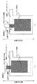
しかしながら、調整用コンデンサは、図7に示すように、表側コンデンサパターンと裏側コンデンサパターンとを、カード基板を挟持して形成した際に重なった部分がコンデンサ領域を形成するため、図8に示すように、カード基板の表裏面に形成されるコンデンサパターンにより得られるコンデンサ領域が、所定の位置に形成されず、コンデンサ領域をアンテナコイルと最終的に連結させるための連結部分に対して水平方向にずれて形成された場合には、そのずれた連結部分の領域に相当するコンデンサ容量が減少または増加してしまうこととなり、所定のコンデンサ容量を保持するコンデンサ領域をカード基板に形成することができない場合がある。例えば、(a)のように、位置ずれ方向(連結部分に対して水平方向を示す)が連結部分側にずれた場合には、そのずれた連結部分の領域に相当するコンデンサ容量が減少してしまう。また、(b)のように、位置ずれ方向(連結部分に対して水平方向を示す)が連結部分と反対側にずれた場合には、そのずれた連結部分の領域に相当するコンデンサ容量が増加してしまう。
【0008】
本発明は、上記事情に鑑みてなされたものであり、位置ずれ等が生じ、カード基板の表裏面に形成されるコンデンサパターンが所定の位置に形成されなくとも、所定のコンデンサ容量を保持するアンテナシート、ICカード及びコンデンサの形成方法を提供することを目的とする。
【0009】
【課題を解決するための手段】
かかる目的を達成するために本発明は以下のような特徴を有する。
請求項1記載の発明は、金属片が絶縁基材を挟んで絶縁基材の表裏面に形成されてなるコンデンサと、絶縁基材の片面に形成されてなるアンテナコイルと、を有するアンテナシートであって、絶縁基材の一方の面に形成される金属片は、絶縁基材の他方の面に形成される金属片よりも小さい領域の金属片であり、小さい領域の金属片は、該金属片を最終的にアンテナコイルに連結させる連結部分が金属片に付設される側とは逆方向となる側に、連結部分と同じ形状の位置ずれ領域を金属片に付設して形成されてなることを特徴とする。
【0010】
請求項2記載の発明は、金属片が絶縁基材を挟んで絶縁基材の表裏面に形成されてなるコンデンサと、絶縁基材の片面に形成されてなるアンテナコイルと、アンテナコイルと接続されたICチップと、を有するICカードであって、絶縁基材の一方の面に形成される金属片は、絶縁基材の他方の面に形成される金属片よりも小さい領域の金属片であり、小さい領域の金属片は、該金属片を最終的にアンテナコイルに連結させる連結部分が金属片に付設される側とは逆方向となる側に、連結部分と同じ形状の位置ずれ領域を金属片に付設して形成されてなることを特徴とする。
【0011】
請求項3記載の発明は、絶縁基材の表裏面にコンデンサとなる金属片を形成するコンデンサの形成方法であって、絶縁基材の一方の面に形成される金属片は、絶縁基材の他方の面に形成される金属片よりも小さい領域の金属片で形成し、且つ、該小さい領域で形成される金属片は、金属片を最終的にアンテナコイルに連結させる連結部分が金属片に付設される側とは逆方向となる側に、連結部分と同じ形状の位置ずれ領域を金属片に付設して形成することを特徴とする。
【0012】
【発明の実施の形態】
以下、添付図面を参照しながら、本発明にかかる実施の形態について説明する。
【0013】
まず、図1を参照しながら非接触ICカードの構成について説明する。
本発明にかかる非接触ICカードは、図1に示すように、絶縁性のカード基板1の周辺部に、螺旋状に形成されたインダクタンスLのアンテナコイル2と、カード基板1上に搭載された合成キャパシタンスCを形成するコンデンサ3と、制御装置、記憶回路、入出力回路等の複数の回路を搭載したICチップ4と、を有して構成されており、共振周波数近辺の周波数を有する電波によりカード基板1上に誘導される電圧が検出され、これにより受信が行われる。
【0014】
短波帯を使用する非接触ICカードは、充分な通信特性を得るために、アンテナコイル2と、コンデンサ3と、からなる同調回路の定数を正確に決定しなければならないが、ICチップ4と、コンデンサ3と、の形成は、その形成工程時において、その容量値に大きなばらつきを発生させている。
【0015】
このような、容量値のばらつきを調整するために、合成キャパシタンスCを形成するコンデンサ3を変化させ、非接触ICカード毎に異なる共振周波数fを設定することとする。
【0016】
なお、LC共振回路の共振周波数は、以下に示される式(1)にて算出されるものである。
【0017】
f=1/2π√(LC)・・・式(1)
【0018】
この式(1)に示すように、共振周波数fは、コンデンサの合成キャパシタンスCと、コイルのインダクタンスLと、の積の平方根に反比例するものである。
【0019】
従って、コンデンサを短絡して、合成キャパシタンスCの容量を減少させることで、共振周波数fを設定している。
【0020】
なお、コンデンサのキャパシタンスCは、図2に示すように、カード基板の表面に形成された表側コンデンサパターンと、カード基板の裏面に形成された裏側コンデンサパターンと、がカード基板を介して対称に位置する領域により形成されるコンデンサ領域S(極板面積)と、カード基板の厚さd(極板間距離)と、で形成され、コンデンサのキャパシタンスCは、以下に示される式(2)にて算出されるものである。なお、αは、ある所定の定数(誘電率)を示す。
【0021】
C=α×S/d・・・式(2)
【0022】
本発明は、共振周波数fを設定するためのコンデンサ部分となる金属片を、カード基板の表裏面に形成した際に、金属片の形成位置がずれた場合でも、所定のコンデンサ容量Cが保持されるために、図3に示すように、コンデンサCとなる金属片を連結する連結部分が付設されている側とは逆方向となる側に、位置ずれが生じた際にコンデンサ容量を補正する位置ずれ領域を付設してカード基板に表側コンデンサパターンを形成する。
【0023】
これにより、図4に示すように、金属片の形成位置が所定の距離Δtだけ、連結部分側にずれた際に、金属片を連結する連結部分の幅r×Δtの面積ΔSにより得られるコンデンサ容量ΔCが減少しても、位置ずれ領域ΔSにて得られるコンデンサ容量ΔCにて補正することが可能となり、所定のコンデンサ容量を保持することが可能となる。
【0024】
また、図5に示すように、金属片の形成位置が所定の距離Δt1だけ、位置ずれ領域側にずれた際に、金属片を連結する連結部分の幅r×Δt1の面積ΔS1により得られるコンデンサ容量ΔC1が増加しても、位置ずれ領域ΔS1にて得られるコンデンサ容量ΔC1にて修正することが可能となり、所定のコンデンサ容量を保持することが可能となる。
【0025】
次に、カード基板の表裏面に形成するコンデンサのパターン形成について説明する。
カード基板に形成するコンデンサパターンは、エッチング等の手法を用いて形成することが好ましい。エッチングは、緻密なコンデンサパターンを正確に形成することが可能であり、さらに、表面抵抗率も低くすることが可能である。以下に、エッチングによるコンデンサパターンの形成方法について説明する。
【0026】
(第1のコンデンサパターンの形成方法)
まず、第1のコンデンサパターンの形成方法について説明する。
第1のコンデンサパターンの形成方法は、絶縁性を有するカード基板の片面に、銅やアルミニウム等の導電性の金属箔を、図3に示すような、位置ずれ領域が付設された表側コンデンサパターンをエッチングにて形成する。また、カード基板の他方の面に、図3に示すような、裏側コンデンサパターンをエッチングにて形成する。そして、表裏面に形成したコンデンサパターンを接続するために、所望の位置に表裏を貫くスルーホールを設け、該設けたスルーホール内に、銀等の導電性ペーストを挿入することにより、表裏面のコンデンサパターンを電気的に導通させる形成方法である。なお、エッチングにてカード基板の両面にコンデンサパターンを形成した際に、スルーホールを設ける方法として、「かしめる」という方法でも適用可能である。
【0027】
このように、第1のコンデンサパターンの形成方法は、エッチング手法を用いて、カード基板の片面に形成するコンデンサパターンの領域を、他方の面に形成するコンデンサパターンの領域よりも小さく、且つ、その小さい領域で形成するコンデンサパターンに位置ずれ領域を付設して形成することで、カード基板に形成するコンデンサパターンの形成位置が所定の距離だけずれた際に変化する連結部分のコンデンサ容量を、位置ずれ領域にて得られるコンデンサ容量にて調整することが可能となり、所定のコンデンサ容量を保持することが可能となる。
【0028】
(第2のコンデンサパターンの形成方法)
次に、第2のコンデンサパターンの形成方法について説明する。
第2のコンデンサパターンの形成方法は、カード基板の片面に、銅やアルミニウム等の導電性の金属箔を、エッチング処理を施して、図3に示すような、位置ずれ領域が付設された表側コンデンサパターンを形成する。また、カード基板の他方の面には、導電性ペーストをスクリーン印刷等を用いて、図3に示すような、裏側コンデンサパターンを形成する。そして、所望の位置に表裏を貫くスルーホールを設け、該設けたスルーホール内に、銀等の導電性ペーストを挿入することにより、表裏面のコンデンサパターンを電気的に導通させるように形成する方法である。なお、エッチング手法を用いて裏側コンデンサパターンを形成し、印刷手法を用いて位置ずれ領域が付設された表側コンデンサパターンを形成することも可能である。
【0029】
このように、第2のコンデンサパターンの形成方法は、エッチング手法と、印刷手法を用いて、カード基板の片面に形成するコンデンサパターンの領域を、他方の面に形成するコンデンサパターンの領域よりも小さく、且つ、小さい領域で形成するコンデンサパターンに位置ずれ領域を付設して形成することで、カード基板に形成するコンデンサパターンの形成位置が所定の距離だけずれた際に変化する連結部分のコンデンサ容量を、位置ずれ領域にて得られるコンデンサ容量にて調整することが可能となり、所定のコンデンサ容量を保持することが可能となる。
【0030】
なお、上記第1及び第2のコンデンサパターンの形成時において、位置ずれ領域を付設して絶縁基材の一方の面に形成される表側コンデンサパターンの形状は、位置ずれ領域が付設されていれば、特に限定せず、例えば、図6に示すようなコンデンサパターンとすることも可能である。
【0031】
なお、上述する実施の形態は、本発明の好適な実施の形態であり、本発明の要旨を逸脱しない範囲内において種々変更実施が可能である。
例えば、本発明のコンデンサパターンは、接触型、非接触型にかかわらず、両面にコンデンサパターンを形成する形式のカード基板であれば適用可能である。
また、コンデンサパターンは、公知の形成方法を用いても形成することは可能である。
【0032】
【発明の効果】
以上の説明より明らかなように本発明は以下のような効果を奏する。
本発明にかかる、アンテナシート、ICカード及びコンデンサの形成方法は、絶縁基材の一方の面に形成される金属片が、絶縁基材の他方の面に形成される金属片よりも小さい領域の金属片で形成されており、且つ、その小さい領域の金属片を最終的にアンテナコイルに連結させる連結部分が形成される側とは逆方向となる側に、連結部分と同じ形状の位置ずれ領域を付設して形成されているため、所定のコンデンサ容量を保持することが可能となる。
【図面の簡単な説明】
【図1】本発明にかかるコンデンサパターンが形成されたICカードの構成を示す図である。
【図2】コンデンサのキャパシタンスCを算出するための説明図であり、(a)は、厚さdのカード基板の表裏面に形成されたコンデンサパターンの断面図を示し、(b)は、表側コンデンサパターンと、裏側コンデンサパターンと、により形成されるコンデンサ領域Sを示す図である。
【図3】本発明にかかる位置ずれ領域を付設して形成されたコンデンサパターンを示す図である。
【図4】金属片の形成位置が所定の距離Δtだけ、連結部分側にずれた場合のコンデンサパターンを示す図である。
【図5】金属片の形成位置が所定の距離Δt1だけ、位置ずれ領域側にずれた場合のコンデンサパターンを示す図である。
【図6】本発明にかかる位置ずれ領域を付設して形成されたコンデンサパターンの変形例を示す図である。
【図7】従来におけるコンデンサパターンから得られるコンデンサ容量を示す図である。
【図8】従来におけるコンデンサパターンの形成位置がずれた際のコンデンサ容量を示す図であり、(a)は、位置ずれ方向が連結部分側にずれた場合のコンデンサ容量を示す図であり、(b)は、位置ずれ方向が連結部分と反対側にずれた場合のコンデンサ容量を示す図である。
【符号の説明】
1 カード基板
2 アンテナコイル
3 コンデンサ
4 ICチップ[0001]
TECHNICAL FIELD OF THE INVENTION
The present invention relates to an antenna sheet having a capacitor, an IC card, and a method for forming a capacitor.
[0002]
[Prior art]
With the development of card technology in recent years, there is an IC card used for a wide range of applications as an information recording medium used for various systems. This IC card has a contact-type IC card in which information writing processing and reading processing are performed by being brought into contact with a dedicated device, and information writing processing and reading processing which are performed only by approaching the dedicated device. There is a non-contact type IC card in which the operation is performed. These IC cards have higher security than magnetic cards and have a large amount of information that can be written on the cards themselves, so that only one card can be used in a multifaceted manner, so that the popularity of these IC cards in the industry is ever increasing. I am following.
[0003]
Among them, in particular, a non-contact type IC card does not need to insert the IC card itself into a dedicated device when performing information writing processing or reading processing, and the handling of the card itself may be convenient, It is rapidly spreading in industry.
[0004]
Further, in recent years, IC cards in which the above-mentioned contact-type IC card and non-contact-type IC card are combined are becoming widespread, and an IC chip that performs information writing processing and reading processing in a contact state has been developed. A hybrid IC card equipped with an IC chip for performing information writing processing and reading processing in a non-contact state, and information writing processing in any of a contact state and a non-contact state And a combination type IC card on which one IC chip capable of performing read processing is mounted.
[0005]
In such an IC card, the tuning constant of a circuit composed of an antenna coil and a resonance capacitor must be accurately determined in order to obtain accurate communication characteristics, and the capacitance of the resonance capacitor is adjusted. Then, it is necessary to perform tuning correction of the circuit, and conventionally, an adjustment capacitor is provided to adjust the resonance frequency (for example, see Patent Document 1).
[0006]
[Patent Document 1]
JP 2001-10264 A
[Problems to be solved by the invention]
However, as shown in FIG. 7, since the adjusting capacitor forms a capacitor region when the front-side capacitor pattern and the back-side capacitor pattern are formed with the card substrate sandwiched therebetween, as shown in FIG. The capacitor region obtained by the capacitor pattern formed on the front and back surfaces of the card board is not formed at a predetermined position, and is shifted in a horizontal direction with respect to a connection portion for finally connecting the capacitor region to the antenna coil. If formed, the capacitor capacity corresponding to the shifted connecting portion area will decrease or increase, and it may not be possible to form a capacitor area holding a predetermined capacitor capacity on the card board. is there. For example, as shown in (a), when the misalignment direction (horizontal direction with respect to the connecting portion) is shifted toward the connecting portion, the capacitor capacity corresponding to the shifted connecting portion region decreases. I will. Further, as shown in (b), when the misalignment direction (shown in the horizontal direction with respect to the connecting portion) is shifted to the opposite side to the connecting portion, the capacitance of the capacitor corresponding to the shifted connecting portion region increases. Resulting in.
[0008]
The present invention has been made in view of the above circumstances, and an antenna that retains a predetermined capacitor capacitance even if a displacement or the like occurs and a capacitor pattern formed on the front and back surfaces of a card substrate is not formed at a predetermined position. It is an object to provide a method for forming a sheet, an IC card, and a capacitor.
[0009]
[Means for Solving the Problems]
To achieve this object, the present invention has the following features.
The invention according to claim 1 is an antenna sheet having a capacitor in which a metal piece is formed on the front and back surfaces of an insulating base with an insulating base therebetween, and an antenna coil formed on one side of the insulating base. The metal piece formed on one surface of the insulating base is a metal piece in an area smaller than the metal piece formed on the other surface of the insulating base, and the metal piece in the small area is the metal piece. The connecting portion that finally connects the piece to the antenna coil is formed by attaching a misalignment area of the same shape to the metal piece on the side opposite to the side attached to the metal piece. It is characterized by.
[0010]
According to a second aspect of the present invention, there is provided a capacitor having metal pieces formed on the front and back surfaces of the insulating base material with the insulating base material interposed therebetween, an antenna coil formed on one surface of the insulating base material, and an antenna coil. An IC card comprising: a metal piece formed on one surface of the insulating base material, the metal piece being a smaller area than the metal piece formed on the other surface of the insulating base material. The metal piece in the small area has a misalignment area of the same shape as the connection part on the side opposite to the side where the connection part that finally connects the metal piece to the antenna coil is attached to the metal piece. It is characterized by being formed so as to be attached to a piece.
[0011]
The invention according to claim 3 is a method for forming a capacitor, in which a metal piece to be a capacitor is formed on the front and back surfaces of the insulating base material, wherein the metal piece formed on one surface of the insulating base material is The metal piece formed in an area smaller than the metal piece formed on the other surface, and the metal piece formed in the small area has a connection portion that finally connects the metal piece to the antenna coil. A misalignment region having the same shape as the connection portion is formed on the metal piece on the side opposite to the side on which the connection is provided.
[0012]
BEST MODE FOR CARRYING OUT THE INVENTION
Hereinafter, embodiments of the present invention will be described with reference to the accompanying drawings.
[0013]
First, the configuration of a non-contact IC card will be described with reference to FIG.
As shown in FIG. 1, a non-contact IC card according to the present invention is mounted on an insulating card substrate 1 around an
[0014]
In the non-contact IC card using the short-wave band, in order to obtain sufficient communication characteristics, the constant of a tuning circuit including the
[0015]
In order to adjust such a variation in the capacitance value, the capacitor 3 forming the combined capacitance C is changed, and a different resonance frequency f is set for each non-contact IC card.
[0016]
The resonance frequency of the LC resonance circuit is calculated by the following equation (1).
[0017]
f = 1 / 2π√ (LC) Equation (1)
[0018]
As shown in the equation (1), the resonance frequency f is inversely proportional to the square root of the product of the combined capacitance C of the capacitor and the inductance L of the coil.
[0019]
Therefore, the resonance frequency f is set by short-circuiting the capacitor and reducing the capacitance of the combined capacitance C.
[0020]
As shown in FIG. 2, the capacitance C of the capacitor is such that the front-side capacitor pattern formed on the front surface of the card substrate and the back-side capacitor pattern formed on the back surface of the card substrate are symmetrically positioned via the card substrate. And the thickness d (distance between the plates) of the card substrate, and the capacitance C of the capacitor is expressed by the following equation (2). It is calculated. Here, α indicates a predetermined constant (dielectric constant).
[0021]
C = α × S / d Equation (2)
[0022]
According to the present invention, when a metal piece serving as a capacitor portion for setting the resonance frequency f is formed on the front and back surfaces of the card substrate, a predetermined capacitor capacitance C is maintained even if the formation position of the metal piece is shifted. Therefore, as shown in FIG. 3, on the side opposite to the side where the connecting portion for connecting the metal pieces serving as the capacitor C is provided, a position for correcting the capacitor capacitance when a positional shift occurs. A shift capacitor area is provided to form a front-side capacitor pattern on the card substrate.
[0023]
As a result, as shown in FIG. 4, when the formation position of the metal piece is shifted toward the connecting portion by a predetermined distance Δt, the capacitor obtained by the area ΔS of the width r × Δt of the connecting portion connecting the metal pieces. Even if the capacitance ΔC decreases, it is possible to correct the capacitance with the capacitor capacitance ΔC obtained in the displacement region ΔS, and to maintain a predetermined capacitance.
[0024]
Further, as shown in FIG. 5, when the formation position of the metal piece is shifted to the position shift area side by a predetermined distance Δt1, the capacitor obtained by the area ΔS1 of the width r × Δt1 of the connecting portion connecting the metal pieces. Even if the capacitance ΔC1 increases, it is possible to correct the capacitance with the capacitor capacitance ΔC1 obtained in the displacement area ΔS1, and to maintain a predetermined capacitance.
[0025]
Next, the pattern formation of the capacitor formed on the front and back surfaces of the card substrate will be described.
The capacitor pattern formed on the card substrate is preferably formed using a technique such as etching. The etching can accurately form a dense capacitor pattern, and can also lower the surface resistivity. Hereinafter, a method of forming a capacitor pattern by etching will be described.
[0026]
(Method of forming first capacitor pattern)
First, a method for forming the first capacitor pattern will be described.
The first method for forming a capacitor pattern is to form a conductive metal foil such as copper or aluminum on one surface of an insulating card substrate and form a front-side capacitor pattern provided with a misalignment region as shown in FIG. It is formed by etching. On the other side of the card substrate, a backside capacitor pattern as shown in FIG. 3 is formed by etching. Then, in order to connect the capacitor pattern formed on the front and back surfaces, a through hole is formed at a desired position, penetrating the front and back surfaces, and a conductive paste such as silver is inserted into the provided through hole, thereby forming the front and back surfaces. This is a forming method for electrically connecting the capacitor pattern. It should be noted that when forming capacitor patterns on both sides of the card substrate by etching, a method of “caulking” can be applied as a method of providing through holes.
[0027]
As described above, in the first method for forming a capacitor pattern, the area of the capacitor pattern formed on one side of the card substrate is smaller than the area of the capacitor pattern formed on the other side by using an etching technique, and By adding a misalignment area to the capacitor pattern formed in a small area, the capacitor capacitance of the connected part, which changes when the formation position of the capacitor pattern formed on the card board is shifted by a predetermined distance, can be misaligned. The adjustment can be performed by the capacitor capacity obtained in the region, and a predetermined capacitor capacity can be maintained.
[0028]
(Method of forming second capacitor pattern)
Next, a method for forming the second capacitor pattern will be described.
A second method for forming a capacitor pattern is to etch a conductive metal foil such as copper or aluminum on one side of a card substrate to form a front-side capacitor having a misaligned region as shown in FIG. Form a pattern. On the other surface of the card substrate, a backside capacitor pattern as shown in FIG. 3 is formed by using a conductive paste by screen printing or the like. Then, a method of forming a through hole penetrating the front and back at a desired position and inserting a conductive paste such as silver into the provided through hole to electrically connect the capacitor pattern on the front and back is formed. It is. Note that it is also possible to form the backside capacitor pattern using an etching technique and form the frontside capacitor pattern provided with the misalignment region using a printing technique.
[0029]
As described above, in the second capacitor pattern forming method, the area of the capacitor pattern formed on one side of the card substrate is made smaller than the area of the capacitor pattern formed on the other side by using the etching technique and the printing technique. In addition, by forming a capacitor pattern formed in a small area with a misalignment area attached thereto, the capacitance of the coupling portion, which changes when the formation position of the capacitor pattern formed on the card board is shifted by a predetermined distance, is reduced. In addition, the adjustment can be performed by the capacitor capacity obtained in the displacement region, and the predetermined capacitor capacity can be maintained.
[0030]
When the first and second capacitor patterns are formed, the shape of the front-side capacitor pattern formed on one surface of the insulating base material with the misalignment region is provided if the misalignment region is additionally provided. The present invention is not particularly limited, and for example, a capacitor pattern as shown in FIG. 6 can be used.
[0031]
The above-described embodiment is a preferred embodiment of the present invention, and various modifications can be made without departing from the spirit of the present invention.
For example, the capacitor pattern of the present invention can be applied to a card substrate of a type in which a capacitor pattern is formed on both sides irrespective of a contact type or a non-contact type.
Also, the capacitor pattern can be formed by using a known forming method.
[0032]
【The invention's effect】
As is clear from the above description, the present invention has the following effects.
According to the method for forming an antenna sheet, an IC card, and a capacitor according to the present invention, the metal piece formed on one surface of the insulating base material has an area smaller than the metal piece formed on the other surface of the insulating base material. A misalignment region having the same shape as the connecting portion is formed on the side opposite to the side on which the connecting portion for finally connecting the small portion of the metal piece to the antenna coil is formed. , It is possible to maintain a predetermined capacitor capacity.
[Brief description of the drawings]
FIG. 1 is a diagram showing a configuration of an IC card on which a capacitor pattern according to the present invention is formed.
FIGS. 2A and 2B are explanatory diagrams for calculating a capacitance C of a capacitor. FIG. 2A is a cross-sectional view of a capacitor pattern formed on the front and back surfaces of a card substrate having a thickness d, and FIG. FIG. 3 is a diagram showing a capacitor region S formed by a capacitor pattern and a back-side capacitor pattern.
FIG. 3 is a view showing a capacitor pattern formed by adding a misalignment region according to the present invention.
FIG. 4 is a diagram illustrating a capacitor pattern when a formation position of a metal piece is shifted toward a connection portion by a predetermined distance Δt.
FIG. 5 is a view showing a capacitor pattern when a formation position of a metal piece is shifted toward a position shift area by a predetermined distance Δt1.
FIG. 6 is a view showing a modified example of a capacitor pattern formed by adding a misalignment region according to the present invention.
FIG. 7 is a diagram showing a capacitor capacity obtained from a conventional capacitor pattern.
8A and 8B are diagrams illustrating a conventional capacitor capacity when the formation position of the capacitor pattern is shifted, and FIG. 8A is a diagram illustrating the capacitor capacity when the position shift direction is shifted to the connecting portion side; (b) is a diagram showing the capacitance of the capacitor when the direction of the displacement is shifted to the side opposite to the connecting portion.
[Explanation of symbols]
1
Claims (3)
前記絶縁基材の一方の面に形成される金属片は、前記絶縁基材の他方の面に形成される金属片よりも小さい領域の金属片であり、
前記小さい領域の金属片は、該金属片を最終的に前記アンテナコイルに連結させる連結部分が前記金属片に付設される側とは逆方向となる側に、前記連結部分と同じ形状の位置ずれ領域を前記金属片に付設して形成されてなることを特徴とするアンテナシート。A capacitor having a metal piece formed on the front and back surfaces of the insulating base material with an insulating base material interposed therebetween, and an antenna coil having an antenna coil formed on one surface of the insulating base material,
The metal piece formed on one surface of the insulating base is a metal piece in a region smaller than the metal piece formed on the other surface of the insulating base,
The metal piece in the small area has a misalignment of the same shape as the connection part on the side where the connection part for finally connecting the metal piece to the antenna coil is in the opposite direction to the side attached to the metal piece. An antenna sheet formed by attaching a region to the metal piece.
前記絶縁基材の一方の面に形成される金属片は、前記絶縁基材の他方の面に形成される金属片よりも小さい領域の金属片であり、
前記小さい領域の金属片は、該金属片を最終的に前記アンテナコイルに連結させる連結部分が前記金属片に付設される側とは逆方向となる側に、前記連結部分と同じ形状の位置ずれ領域を前記金属片に付設して形成されてなることを特徴とするICカード。A capacitor in which a metal piece is formed on the front and back surfaces of the insulating base with the insulating base interposed therebetween, an antenna coil formed on one side of the insulating base, and an IC chip connected to the antenna coil; An IC card having
The metal piece formed on one surface of the insulating base is a metal piece in a region smaller than the metal piece formed on the other surface of the insulating base,
The metal piece in the small area has a misalignment of the same shape as the connection part on the side where the connection part for finally connecting the metal piece to the antenna coil is in the opposite direction to the side attached to the metal piece. An IC card comprising an area attached to the metal piece.
前記絶縁基材の一方の面に形成される金属片は、前記絶縁基材の他方の面に形成される金属片よりも小さい領域の金属片で形成し、且つ、該小さい領域で形成される金属片は、前記金属片を最終的に前記アンテナコイルに連結させる連結部分が前記金属片に付設される側とは逆方向となる側に、前記連結部分と同じ形状の位置ずれ領域を前記金属片に付設して形成することを特徴とするコンデンサの形成方法。A method for forming a capacitor that forms a metal piece to be a capacitor on the front and back surfaces of an insulating base material,
The metal piece formed on one surface of the insulating base material is formed of a metal piece in an area smaller than the metal piece formed on the other surface of the insulating base material, and is formed in the small area. The metal piece has a misalignment region of the same shape as the connection part on the side where the connection part for finally connecting the metal piece to the antenna coil is in the opposite direction to the side attached to the metal piece. A method for forming a capacitor, wherein the capacitor is formed by attaching to a piece.
Priority Applications (1)
| Application Number | Priority Date | Filing Date | Title |
|---|---|---|---|
| JP2003155378A JP2004357203A (en) | 2003-05-30 | 2003-05-30 | Antenna sheet, ic card, and forming method of capacitor |
Applications Claiming Priority (1)
| Application Number | Priority Date | Filing Date | Title |
|---|---|---|---|
| JP2003155378A JP2004357203A (en) | 2003-05-30 | 2003-05-30 | Antenna sheet, ic card, and forming method of capacitor |
Publications (1)
| Publication Number | Publication Date |
|---|---|
| JP2004357203A true JP2004357203A (en) | 2004-12-16 |
Family
ID=34049771
Family Applications (1)
| Application Number | Title | Priority Date | Filing Date |
|---|---|---|---|
| JP2003155378A Withdrawn JP2004357203A (en) | 2003-05-30 | 2003-05-30 | Antenna sheet, ic card, and forming method of capacitor |
Country Status (1)
| Country | Link |
|---|---|
| JP (1) | JP2004357203A (en) |
Cited By (2)
| Publication number | Priority date | Publication date | Assignee | Title |
|---|---|---|---|---|
| JP2009288874A (en) * | 2008-05-27 | 2009-12-10 | Mitsubishi Electric Corp | Radio communication apparatus |
| KR20120080601A (en) * | 2009-09-18 | 2012-07-17 | 테크놀로지안 투트키무스케스쿠스 브이티티 | Antenna construction, for example for an rfid transponder system |
-
2003
- 2003-05-30 JP JP2003155378A patent/JP2004357203A/en not_active Withdrawn
Cited By (5)
| Publication number | Priority date | Publication date | Assignee | Title |
|---|---|---|---|---|
| JP2009288874A (en) * | 2008-05-27 | 2009-12-10 | Mitsubishi Electric Corp | Radio communication apparatus |
| KR20120080601A (en) * | 2009-09-18 | 2012-07-17 | 테크놀로지안 투트키무스케스쿠스 브이티티 | Antenna construction, for example for an rfid transponder system |
| JP2013505618A (en) * | 2009-09-18 | 2013-02-14 | テクノロギアン トゥトキムスケスクス ヴェーテーテー | Antenna for RFID transponder system |
| KR101657157B1 (en) * | 2009-09-18 | 2016-09-19 | 테크놀로지안 투트키무스케스쿠스 브이티티 오와이 | Antenna construction, for example for an RFID transponder system |
| US9502749B2 (en) | 2009-09-18 | 2016-11-22 | Teknologian Tutkimuskeskus Vtt Oy | Antenna construction, for example for an RFID transponder system |
Similar Documents
| Publication | Publication Date | Title |
|---|---|---|
| JP4641096B2 (en) | Non-contact data carrier device and wiring member for booster antenna | |
| US5999409A (en) | Contactless IC card | |
| US6879258B2 (en) | IC card having a mica film for stable resonance frequency and enhanced antenna properties | |
| US10396429B2 (en) | Wireless communication device | |
| TWI683473B (en) | Non-contact communication antenna, communication device, and method for manufacturing non-contact communication antenna | |
| JP2005129019A (en) | Ic card | |
| JP2006262055A (en) | Antenna module and portable information terminal provided with the same | |
| JP2010063007A (en) | Electromagnetic induction module | |
| JP2005165703A (en) | Non-contact identification medium | |
| JP4302859B2 (en) | Non-contact IC tag | |
| JP2004206479A (en) | Non-contact tag | |
| JP4562892B2 (en) | Non-contact data carrier device and wiring member for booster antenna | |
| JPH11353440A (en) | Capacitor and noncontact type ic card | |
| JP2004357203A (en) | Antenna sheet, ic card, and forming method of capacitor | |
| JP2010028351A (en) | Booster antenna and contactless information medium | |
| JP5975259B2 (en) | Non-contact IC mounting substrate and non-contact IC card | |
| JP2004021484A (en) | Auxiliary antenna member for non-contact data-carrier apparatus and built-in bag thereof | |
| JP2007311407A (en) | Ic chip, wafer finished with circuit formation, and noncontact communication member | |
| JP2012094948A (en) | Inlet for non-contact communication recording medium, method of manufacturing the same, and non-contact communication recording medium | |
| JP4641095B2 (en) | Non-contact data carrier device and wiring member for booster antenna | |
| JP2004364143A (en) | Antenna sheet, ic card, and method for forming capacitor | |
| JP2003006589A (en) | Non-contact communication recording medium and manufacturing method therefor | |
| JP6984362B2 (en) | Inlet and non-contact communication medium | |
| JP2003173426A (en) | Id tag and id tag characteristic adjusting method | |
| JP2002049899A (en) | Coil wiring/arranging member, and data carrier device |
Legal Events
| Date | Code | Title | Description |
|---|---|---|---|
| A300 | Application deemed to be withdrawn because no request for examination was validly filed |
Free format text: JAPANESE INTERMEDIATE CODE: A300 Effective date: 20060801 |