JP2004343116A - Lithography equipment, method of manufacturing device, and device manufactured thereby - Google Patents
Lithography equipment, method of manufacturing device, and device manufactured thereby Download PDFInfo
- Publication number
- JP2004343116A JP2004343116A JP2004142232A JP2004142232A JP2004343116A JP 2004343116 A JP2004343116 A JP 2004343116A JP 2004142232 A JP2004142232 A JP 2004142232A JP 2004142232 A JP2004142232 A JP 2004142232A JP 2004343116 A JP2004343116 A JP 2004343116A
- Authority
- JP
- Japan
- Prior art keywords
- mirror
- shield
- heat
- support structure
- radiation
- Prior art date
- Legal status (The legal status is an assumption and is not a legal conclusion. Google has not performed a legal analysis and makes no representation as to the accuracy of the status listed.)
- Granted
Links
Images


Classifications
-
- G—PHYSICS
- G03—PHOTOGRAPHY; CINEMATOGRAPHY; ANALOGOUS TECHNIQUES USING WAVES OTHER THAN OPTICAL WAVES; ELECTROGRAPHY; HOLOGRAPHY
- G03F—PHOTOMECHANICAL PRODUCTION OF TEXTURED OR PATTERNED SURFACES, e.g. FOR PRINTING, FOR PROCESSING OF SEMICONDUCTOR DEVICES; MATERIALS THEREFOR; ORIGINALS THEREFOR; APPARATUS SPECIALLY ADAPTED THEREFOR
- G03F7/00—Photomechanical, e.g. photolithographic, production of textured or patterned surfaces, e.g. printing surfaces; Materials therefor, e.g. comprising photoresists; Apparatus specially adapted therefor
- G03F7/20—Exposure; Apparatus therefor
-
- G—PHYSICS
- G03—PHOTOGRAPHY; CINEMATOGRAPHY; ANALOGOUS TECHNIQUES USING WAVES OTHER THAN OPTICAL WAVES; ELECTROGRAPHY; HOLOGRAPHY
- G03F—PHOTOMECHANICAL PRODUCTION OF TEXTURED OR PATTERNED SURFACES, e.g. FOR PRINTING, FOR PROCESSING OF SEMICONDUCTOR DEVICES; MATERIALS THEREFOR; ORIGINALS THEREFOR; APPARATUS SPECIALLY ADAPTED THEREFOR
- G03F7/00—Photomechanical, e.g. photolithographic, production of textured or patterned surfaces, e.g. printing surfaces; Materials therefor, e.g. comprising photoresists; Apparatus specially adapted therefor
- G03F7/70—Microphotolithographic exposure; Apparatus therefor
- G03F7/708—Construction of apparatus, e.g. environment aspects, hygiene aspects or materials
- G03F7/70808—Construction details, e.g. housing, load-lock, seals or windows for passing light in or out of apparatus
- G03F7/70825—Mounting of individual elements, e.g. mounts, holders or supports
-
- G—PHYSICS
- G03—PHOTOGRAPHY; CINEMATOGRAPHY; ANALOGOUS TECHNIQUES USING WAVES OTHER THAN OPTICAL WAVES; ELECTROGRAPHY; HOLOGRAPHY
- G03F—PHOTOMECHANICAL PRODUCTION OF TEXTURED OR PATTERNED SURFACES, e.g. FOR PRINTING, FOR PROCESSING OF SEMICONDUCTOR DEVICES; MATERIALS THEREFOR; ORIGINALS THEREFOR; APPARATUS SPECIALLY ADAPTED THEREFOR
- G03F7/00—Photomechanical, e.g. photolithographic, production of textured or patterned surfaces, e.g. printing surfaces; Materials therefor, e.g. comprising photoresists; Apparatus specially adapted therefor
- G03F7/70—Microphotolithographic exposure; Apparatus therefor
- G03F7/708—Construction of apparatus, e.g. environment aspects, hygiene aspects or materials
- G03F7/70808—Construction details, e.g. housing, load-lock, seals or windows for passing light in or out of apparatus
- G03F7/70833—Mounting of optical systems, e.g. mounting of illumination system, projection system or stage systems on base-plate or ground
-
- G—PHYSICS
- G03—PHOTOGRAPHY; CINEMATOGRAPHY; ANALOGOUS TECHNIQUES USING WAVES OTHER THAN OPTICAL WAVES; ELECTROGRAPHY; HOLOGRAPHY
- G03F—PHOTOMECHANICAL PRODUCTION OF TEXTURED OR PATTERNED SURFACES, e.g. FOR PRINTING, FOR PROCESSING OF SEMICONDUCTOR DEVICES; MATERIALS THEREFOR; ORIGINALS THEREFOR; APPARATUS SPECIALLY ADAPTED THEREFOR
- G03F7/00—Photomechanical, e.g. photolithographic, production of textured or patterned surfaces, e.g. printing surfaces; Materials therefor, e.g. comprising photoresists; Apparatus specially adapted therefor
- G03F7/70—Microphotolithographic exposure; Apparatus therefor
- G03F7/708—Construction of apparatus, e.g. environment aspects, hygiene aspects or materials
- G03F7/70858—Environment aspects, e.g. pressure of beam-path gas, temperature
- G03F7/70883—Environment aspects, e.g. pressure of beam-path gas, temperature of optical system
- G03F7/70891—Temperature
-
- G—PHYSICS
- G03—PHOTOGRAPHY; CINEMATOGRAPHY; ANALOGOUS TECHNIQUES USING WAVES OTHER THAN OPTICAL WAVES; ELECTROGRAPHY; HOLOGRAPHY
- G03F—PHOTOMECHANICAL PRODUCTION OF TEXTURED OR PATTERNED SURFACES, e.g. FOR PRINTING, FOR PROCESSING OF SEMICONDUCTOR DEVICES; MATERIALS THEREFOR; ORIGINALS THEREFOR; APPARATUS SPECIALLY ADAPTED THEREFOR
- G03F7/00—Photomechanical, e.g. photolithographic, production of textured or patterned surfaces, e.g. printing surfaces; Materials therefor, e.g. comprising photoresists; Apparatus specially adapted therefor
- G03F7/70—Microphotolithographic exposure; Apparatus therefor
- G03F7/708—Construction of apparatus, e.g. environment aspects, hygiene aspects or materials
- G03F7/70858—Environment aspects, e.g. pressure of beam-path gas, temperature
- G03F7/709—Vibration, e.g. vibration detection, compensation, suppression or isolation
-
- G—PHYSICS
- G03—PHOTOGRAPHY; CINEMATOGRAPHY; ANALOGOUS TECHNIQUES USING WAVES OTHER THAN OPTICAL WAVES; ELECTROGRAPHY; HOLOGRAPHY
- G03F—PHOTOMECHANICAL PRODUCTION OF TEXTURED OR PATTERNED SURFACES, e.g. FOR PRINTING, FOR PROCESSING OF SEMICONDUCTOR DEVICES; MATERIALS THEREFOR; ORIGINALS THEREFOR; APPARATUS SPECIALLY ADAPTED THEREFOR
- G03F7/00—Photomechanical, e.g. photolithographic, production of textured or patterned surfaces, e.g. printing surfaces; Materials therefor, e.g. comprising photoresists; Apparatus specially adapted therefor
- G03F7/70—Microphotolithographic exposure; Apparatus therefor
- G03F7/708—Construction of apparatus, e.g. environment aspects, hygiene aspects or materials
- G03F7/70991—Connection with other apparatus, e.g. multiple exposure stations, particular arrangement of exposure apparatus and pre-exposure and/or post-exposure apparatus; Shared apparatus, e.g. having shared radiation source, shared mask or workpiece stage, shared base-plate; Utilities, e.g. cable, pipe or wireless arrangements for data, power, fluids or vacuum
Abstract
Description
本発明は、
− 放射線の投影ビームを供給する放射線システムと、
− 所望するパターンに従って投影ビームをパターン化するパターニング手段を支持する支持装置と、
− 基板を保持する基板テーブルと、
− パターン化されたビームを基板の目標部分に投影する投影システムとから成るリソグラフィ投影装置に関する。
The present invention
A radiation system for providing a projection beam of radiation;
A support device for supporting a patterning means for patterning the projection beam according to a desired pattern;
A substrate table for holding the substrate;
A projection system for projecting the patterned beam onto a target portion of the substrate.
本明細書において使用する「パターニング手段」なる用語は、入射する放射線ビームに、基板の目標部分に作り出されるべきパターンと一致するパターン化断面を与えるために使用し得る手段に当たるものとして広義に解釈されるべきである。また、「ライトバルブ」なる用語もこうした状況において使用される。一般的に、上記のパターンは、集積回路や他のデバイス(以下を参照)であるような、デバイスにおいて目標部分に作り出される特別な機能層に相当する。そのようなパターニング手段には以下が含まれる。すなわち、
− マスク。マスクの概念はリソグラフィにおいて周知のものであり、これには、様々なハイブリッドマスクタイプのみならず、バイナリマスク、レベンソンマスク、減衰位相シフトマスクといったようなマスクタイプも含まれる。放射線ビームにこのようなマスクを配置することにより、マスクに照射する放射線の、マスクパターンに従う選択的透過(透過性マスクの場合)や選択的反射(反射性マスクの場合)を可能にする。マスクの場合、その支持構造は一般的に、入射する放射線ビームの所望する位置にマスクを保持しておくことが可能であり、かつ、必要な場合、ビームに対して運動させることの可能なマスクテーブルである。
− プログラマブルミラーアレイ。このようなデバイスの一例として、粘弾性制御層および反射面を有するマトリクスアドレス可能面があげられる。こうした装置の基本的原理は、(例えば)反射面のアドレスされた領域は入射光を回折光として反射するが、アドレスされていない領域は入射光を非回折光として反射するといったことである。適切なフィルタを使用することにより、回折光のみを残して上記非回折光を反射ビームからフィルタすることが可能である。この方法において、ビームはマトリクスアドレス可能面のアドレスパターンに従ってパターン形成される。プログラマブルミラーアレイのまた別の実施形態では小さな複数のミラーのマトリクス配列を用いる。そのミラーの各々は、適した局部電界を適用することによって、もしくは圧電作動手段を用いることによって、軸を中心に個々に傾けられている。もう一度言うと、ミラーはマトリクスアドレス可能であり、それによりアドレスされたミラーはアドレスされていないミラーとは異なる方向に入射の放射線ビームを反射する。このようにして、反射されたビームはマトリクスアドレス可能ミラーのアドレスパターンに従いパターン形成される。必要とされるマトリクスアドレッシングは適切な電子手段を用いて実行される。前述した両ケースとも、パターニング手段は1つ以上のプログラマブルミラーアレイから構成可能である。ミラーアレイに関する詳細は、例えば、米国特許第US5,296,891号および同第US5,523,193号、並びに、PCT特許種出願第WO98/38597および同WO98/33096を参照されたい。これらの内容を本明細書に引用したものとする。プログラマブルミラーアレイの場合、上記支持構造は、例えばフレームもしくはテーブルとして具体化され、これは必要に応じて、固定式となるか、もしくは可動式となる。
− プログラマブルLCDアレイ。このような構成の例の詳細は米国特許第US5,229,872号を参照されたい。上記同様、この場合における支持構造も、例えばフレームもしくはテーブルとして具体化され、これも必要に応じて、固定式となるか、もしくは可動式となる。簡潔化の目的で、本文の残りを、特定の箇所において、マスクおよびマスクテーブルを必要とする例に限定して導くものとする。しかし、こうした例において論じられる一般的な原理は、既に述べたようなパターニング手段のより広範な状況において理解されるべきである。
The term "patterning means" as used herein is to be interpreted broadly as referring to means that can be used to impart an incoming radiation beam with a patterned cross-section that matches the pattern to be created on the target portion of the substrate. Should be. The term "light valve" is also used in such situations. Generally, the above patterns will correspond to special functional layers that are created in a target portion of the device, such as an integrated circuit or other device (see below). Such patterning means include the following. That is,
A mask. The concept of a mask is well known in lithography, and includes various hybrid mask types as well as mask types such as binary masks, Levenson masks, and attenuated phase shift masks. By arranging such a mask in the radiation beam, it is possible to selectively transmit (in the case of a transmissive mask) or selectively reflect (in the case of a reflective mask) the radiation applied to the mask according to the mask pattern. In the case of a mask, the support structure is generally capable of holding the mask in a desired position of the incoming radiation beam and, if necessary, being movable with respect to the beam. It is a table.
A programmable mirror array. One example of such a device is a matrix-addressable surface having a viscoelastic control layer and a reflective surface. The basic principle of such a device is that (for example) the addressed areas of the reflective surface reflect the incident light as diffracted light, while the unaddressed areas reflect the incident light as undiffracted light. By using an appropriate filter, it is possible to filter out the undiffracted light from the reflected beam, leaving only the diffracted light. In this method, the beam is patterned according to an address pattern on a matrix-addressable surface. Yet another embodiment of a programmable mirror array uses a matrix arrangement of small mirrors. Each of the mirrors is individually tilted about an axis by applying a suitable local electric field or by using piezoelectric actuation means. Once again, the mirrors are matrix-addressable, such that addressed mirrors will reflect an incoming radiation beam in a different direction than unaddressed mirrors. In this way, the reflected beam is patterned according to the address pattern of the matrix-addressable mirror. The required matrix addressing is performed using suitable electronic means. In both cases described above, the patterning means can be comprised of one or more programmable mirror arrays. For more information on mirror arrays, see, for example, US Pat. These contents are cited in this specification. In the case of a programmable mirror array, the support structure is embodied, for example, as a frame or a table, which may be fixed or movable as required.
A programmable LCD array. See US Pat. No. 5,229,872 for details of an example of such an arrangement. As above, the support structure in this case is also embodied as a frame or table, for example, which may be fixed or movable as required. For purposes of brevity, the rest of this text will, at certain locations, direct itself to examples requiring a mask and mask table. However, the general principles discussed in these examples should be understood in the broader context of patterning means as already mentioned.
リソグラフィ投影装置は例えば、集積回路(IC)の製造において使用可能である。この場合、パターニング手段はICの個々の層に対応する回路パターンを生成する。そして、放射線感光材料(レジスト)の層が塗布された基板(シリコンウェハ)上の目標部分(例えば1つあるいはそれ以上のダイから成る)にこのパターンを像形成することが出来る。一般的に、シングルウェハは、投影システムを介して1つずつ順次照射される近接目標部分の全体ネットワークを含んでいる。マスクテーブル上のマスクによるパターニングを用いる現在の装置は、異なる2つのタイプのマシンに区分される。リソグラフィ投影装置の一タイプでは、全体マスクパターンを目標部分に1回の作動にて露光することによって各目標部分が照射される。こうした装置は一般的にウェハステッパあるいはステップアンドリピート装置と称されている。ステップアンドスキャン装置と称される別の装置では、所定の基準方向(「スキャニング」方向)にマスクパターンを投影ビーム下で徐々にスキャニングし、これと同時に基板テーブルをこの方向と平行に、あるいは反平行にスキャニングすることにより、各目標部分が照射される。一般的に、投影装置は倍率係数M(一般的に、<1)を有することから、基板テーブルが走査される速度Vは、マスクテーブルが走査される速度の係数M倍となる。ここに記載を行ったリソグラフィデバイスの詳細は、例えば、米国特許第US6,046,792号を参照されたい。 A lithographic projection apparatus can be used, for example, in the manufacture of integrated circuits (ICs). In this case, the patterning means generates circuit patterns corresponding to individual layers of the IC. This pattern can then be imaged on a target portion (eg, consisting of one or more dies) on a substrate (silicon wafer) coated with a layer of radiation-sensitive material (resist). In general, a single wafer will contain a whole network of adjacent target portions that are successively irradiated via the projection system, one at a time. Current equipment using patterning by a mask on a mask table is divided into two different types of machines. In one type of lithographic projection apparatus, each target portion is irradiated by exposing the entire mask pattern to the target portion in a single operation. Such an apparatus is generally called a wafer stepper or a step-and-repeat apparatus. In another apparatus, referred to as a step-and-scan apparatus, the mask pattern is gradually scanned under a projection beam in a predetermined reference direction (the "scanning" direction), while the substrate table is being moved parallel to or in this direction. By scanning in parallel, each target portion is illuminated. Generally, since the projection apparatus has a magnification factor M (generally <1), the speed V at which the substrate table is scanned is a factor M times the speed at which the mask table is scanned. For details of the lithographic devices described herein, see, for example, US Pat. No. 6,046,792.
リソグラフィ投影装置を使用する製造工程において、パターン(例えばマスクにおける)は少なくとも部分的に放射線感光材(レジスト)の層で覆われた基板上に像形成される。この像形成ステップに先立ち、基板は、プライミング、レジスト塗布、およびソフトベークといったような各種の工程を経る。露光後、基板は、ポストベーク(PEB)、現像、ハードベーク、および像形成フューチャの測定/検査といったような他の工程を通る。この一連の工程は、例えばICといったような素子の個々の層をパターン化するための基準として使用される。このようなパターン形成された層は、それから、全て個々の層を仕上げる目的である、エッチング、イオン注入(ドーピング)、メタライゼーション、酸化、化学機械的研磨等といった種々のプロセスを経る。数枚の層が必要とされる場合には、全工程、もしくはその変形をそれぞれの新しい層に繰り返す必要がある。最終的に、素子のアレイが基板(ウェハ)上に形成される。次に、これらの素子はダイシングやソーイングといったような技法で相互より分離される。それから個々の素子は、キャリアに装着されたり、ピンに接続されたりし得る。こうした工程に関する詳細は、1997年にマグローヒル出版会社より刊行された、Peter van Zant著、「マイクロチップ製造:半導体処理に対する実用ガイド」という名称の書籍(“Microchip Fabrication:A Pratical Guide to Semiconductor Processing”)の第3版、ISBN0−07−067250−4より入手可能である。この内容をここに引用したものとする。 In a manufacturing process using a lithographic projection apparatus, a pattern (eg, in a mask) is imaged onto a substrate that is at least partially covered by a layer of radiation-sensitive material (resist). Prior to this image forming step, the substrate undergoes various processes such as priming, resist coating, and soft baking. After exposure, the substrate goes through other steps such as post bake (PEB), development, hard bake, and measurement / inspection of the imaging features. This series of steps is used as a basis for patterning individual layers of a device, for example an IC. Such patterned layers then undergo various processes, such as etching, ion implantation (doping), metallization, oxidation, chemical mechanical polishing, etc., all of which are intended to finish the individual layers. If several layers are required, the entire process, or a variant thereof, must be repeated for each new layer. Eventually, an array of devices will be formed on the substrate (wafer). These elements are then separated from one another by techniques such as dicing and sawing. The individual elements can then be mounted on a carrier or connected to pins. Details on these steps are described in a book entitled "Microchip Fabrication: A Practical Guide to Semiconductor Processing" by Peter Van Zant, published by McGraw-Hill Publishing Company in 1997. 3rd Edition, ISBN 0-07-067250-4. This content is quoted here.
簡潔化の目的で、これより投影システムを「レンズ」と称するものとする。しかし、この用語は、例えば屈折光学システム、反射光学システム、および反射屈折光学システムを含むさまざまなタイプの投影システムを網羅するものとして広義に解釈されるべきである。放射線システムはまた、放射線の投影ビームの誘導、成形、あるいは制御を行う、こうした設計タイプのいずれかに応じて稼動する構成要素も備えることが出来る。こうした構成要素もまた以降において集約的に、あるいは単独的に「レンズ」と称する。さらに、リソグラフィ装置は2つあるいはそれ以上の基板テーブル(および、あるいは2つもしくはそれ以上のマスクテーブル)を有するタイプのものである。このような「多段」デバイスにおいては、追加のテーブルが並列して使用される。もしくは、1つ以上の他のテーブルが露光に使用されている間に予備工程が1つ以上のテーブルにて実行される。例えば、米国特許第US5,969,441号および国際特許出願第WO98/40791号に開示のデュアルステージリソグラフィ装置がある。 For the sake of brevity, the projection system will hereinafter be referred to as a "lens". However, the term should be interpreted broadly to cover various types of projection systems, including, for example, refractive, catadioptric, and catadioptric systems. The radiation system can also include components that operate according to any of these design types to steer, shape, or control the projection beam of radiation. Such components will also be referred to hereinafter collectively or solely as "lenses". Further, the lithographic apparatus is of a type having two or more substrate tables (and / or two or more mask tables). In such "multi-stage" devices, additional tables are used in parallel. Alternatively, a preliminary step is performed on one or more tables while one or more other tables are being used for exposure. For example, there is a dual stage lithographic apparatus disclosed in US Pat. No. 5,969,441 and International Patent Application No. WO 98/40791.
欧州特許出願番号第1178357号により、構成要素の大部分が真空チャンバ内に配置されたリソグラフィ装置が知られている。投影ビームは、レンズではなく、多数の光学活性ミラーを介してマスクを基板上に結像する。こうした構成は、例えば、EUV(極紫外線)投影ビームが使用される場合に必要とされる。なぜならば、空気圧においてガス内のEUV投影ビームは投影目的には実用にならず、かつ、EUV放射線に使用可能な屈折光学素子がないという理由による。これは他のタイプのビームでも同じ状況である。 European Patent Application No. 1 178 357 discloses a lithographic apparatus in which most of the components are arranged in a vacuum chamber. The projection beam images the mask onto the substrate via a number of optically active mirrors, rather than a lens. Such a configuration is required, for example, when an EUV (extreme ultraviolet) projection beam is used. This is because, at pneumatic pressure, EUV projection beams in gas are not practical for projection purposes and there are no refractive optics available for EUV radiation. This is the same situation for other types of beams.
欧州特許出願番号第1178357号において、真空下での稼動は、温度安定性に問題を生じる場合があることを指摘している。なぜならば、真空チャンバの壁からの、もしくは真空ポンプからの熱放射が熱膨張または収縮をまねくおそれがあるからである。支持構造、基板テーブル、投影システム、あるいは基準フレームといったような温度クリティカルな構成要素が影響をうけると、それにより結像誤差をまねく。EP1178357では、効果的な熱シールドである「温度調整部材」を使用し、これを熱源と温度クリティカルな構成要素間に配置することでこの問題に対処している。等温に保たれなくてはならない温度クリティカルな構成要素の少なくとも部分を熱シールドで囲む。一実施例において、熱シールドは、温度クリティカルな構成要素に面した側で高い吸収を有し、熱シールドからの放射線の入射により、温度クリティカルな構成要素の温度を調整する。EP1178357では、「調整」により、単にシールドからの放射線が温度にデリケートな構成要素の温度を安定させるという意味にとれる。能動的温度制御ループは示されておらない。 In European Patent Application No. 1178357, it is pointed out that operation under vacuum may cause problems in temperature stability. This is because heat radiation from the walls of the vacuum chamber or from the vacuum pump can lead to thermal expansion or contraction. When temperature-critical components such as the support structure, substrate table, projection system, or reference frame are affected, they lead to imaging errors. EP 1 178 357 addresses this problem by using an effective heat shield, the "temperature regulating member", which is placed between the heat source and the temperature-critical components. A heat shield surrounds at least a portion of the temperature-critical components that must be kept isothermal. In one embodiment, the heat shield has a high absorption on the side facing the temperature critical component, and the incidence of radiation from the heat shield regulates the temperature of the temperature critical component. In EP 1 178 357, "adjustment" means that the radiation from the shield merely stabilizes the temperature of components sensitive to temperature. The active temperature control loop is not shown.
当然ながら、このタイプの解決法は、熱シールドこれ自体が任意温度まで加熱されない場合にのみ効果的である。EP1178357では、強い熱源が存在するなかでいかにこれが達成され得るかを述べていない。さらに、投影システムにおける投影ビームからの放射線の吸収により、投影システムそれ自体が温度クリティカルな構成要素になると同時に熱源にもなるため、全ての熱源と温度クリティカルな構成要素間に熱シールドを配置することは不可能である。 Of course, this type of solution is only effective if the heat shield itself is not heated to any temperature. EP 1 178 357 does not state how this can be achieved in the presence of a strong heat source. In addition, the placement of heat shields between all heat sources and temperature-critical components, as the radiation absorption from the projection beam in the projection system makes the projection system itself a temperature-critical component as well as a heat source. Is impossible.
原理的に、例えば、流体冷却、熱パイプを使用する冷却、あるいは熱輸送を行う他の方法といったような強制熱伝達が、温度クリティカルな構成要素の温度調整に使用され得る。こうした強制熱伝達が、温度を安定維持させるために制御ループにより調整可能であることもまた望ましい。しかし、このタイプの熱伝達が投影システムに適用されると、例えば、強制冷却、あるいは必要な機械的連結により機械的振動をまねき、結像誤差を生じる場合がある。より高い冷却能力が必要とされる場合にこうした問題は重大となる。 In principle, forced heat transfer, such as, for example, fluid cooling, cooling using heat pipes, or other methods of providing heat transfer, can be used to regulate the temperature of critical components. It is also desirable that such forced heat transfer be adjustable by a control loop to maintain a stable temperature. However, when this type of heat transfer is applied to the projection system, it can lead to mechanical vibrations, for example due to forced cooling or the required mechanical coupling, leading to imaging errors. These problems are exacerbated when higher cooling capacity is required.
本発明は、熱伝達による機械的振動の影響を最小限に抑えながら、強制熱伝達によりリソグラフィ装置の投影システムの温度安定性をより確実にすることを目的とする。 It is an object of the present invention to further ensure the temperature stability of a projection system of a lithographic apparatus by means of forced heat transfer, while minimizing the effects of mechanical vibrations due to heat transfer.
本発明は、制御ループの使用を可能にして、投影システムに影響を与える温度を調整することをまた別の目標とする。 The present invention is another aim to enable the use of a control loop to regulate the temperature affecting the projection system.
本発明は、リソグラフィ装置の投影システムにおいて、投影ビームの吸収による熱問題を減じることをまた別の目標とする。 The invention further aims at reducing thermal problems due to absorption of the projection beam in the projection system of the lithographic apparatus.
本発明は、請求項1において説明したようなリソグラフィ装置を提供する。投影システムのミラーおよび/またはこれらミラーの支持構造が熱シールドによりシールドされる。この熱シールドの熱調整に、強制熱伝達回路を使用する。好ましくは、熱伝達回路は、熱シールドに直接、もしくは間接的に連結を行った熱伝播流体を輸送するパイプから成る。(一般的に、熱伝達は熱シールドの純冷却効果を有するが、代替的に、熱伝達は温度が上昇しすぎた場合に低減される純加熱効果を有する。)熱シールドは、ミラーおよびミラーの支持構造とは別々に支持される。その結果、ミラーに及ぼす強制冷却による振動の影響はわずかでしかない。好ましくは、熱シールドと、ミラーおよびミラーの支持構造の共通の支持は共通の計測フレームとなるか、もしくは、計測フレームを介してミラーを支持する他のフレーム上にある。一実施例において、熱シールドと支持構造は計測フレームにより支持され、熱シールドと支持構造あるいはミラー間にその他の機械的連結はなされていない。 The present invention provides a lithographic apparatus as set forth in claim 1. The mirrors of the projection system and / or their support structure are shielded by a heat shield. A forced heat transfer circuit is used for heat adjustment of the heat shield. Preferably, the heat transfer circuit comprises a pipe for transporting a heat-carrying fluid that is directly or indirectly connected to the heat shield. (Generally, heat transfer has the net cooling effect of a heat shield, but alternatively, heat transfer has the net heating effect that is reduced if the temperature is too high.) The heat shield is a mirror and a mirror. Is supported separately from the supporting structure. As a result, the effect of forced vibration on the mirror is minimal. Preferably, the common support of the heat shield, the mirror and the support structure of the mirror is on a common measurement frame or on another frame supporting the mirror via the measurement frame. In one embodiment, the heat shield and the support structure are supported by a metrology frame, and no other mechanical connection is made between the heat shield and the support structure or mirror.
熱シールドは、ミラーおよび/または支持構造への、あるいはミラーおよび/または支持構造からの熱放射を遮断する。好ましくは、熱シールドはシールドされる支持構造への、あるいはシールドされる支持構造からの熱放射の大部分を(少なくとも50%、望ましくは80%を上回り)遮断し、かつ、保護されている支持構造あるいはミラーへの/からのものでない遮断される熱放射は、わずかなものであるように該熱シールドは形成され、配置される。好ましくは、このようにしてそれぞれの熱シールドの各々は出来るかぎり他の全ての構成要素から、それぞれのミラーあるいは支持構造の部分のみをシールドする。 The heat shield blocks thermal radiation to or from the mirror and / or support structure. Preferably, the heat shield blocks most (at least 50%, preferably more than 80%) of the heat radiation to or from the shielded support structure, and the support is protected. The heat shield is formed and arranged such that heat radiation that is not blocked to / from the structure or mirror is negligible. Preferably, each of the respective heat shields in this way shields only a portion of the respective mirror or support structure from all other components as far as possible.
よって、振動の量を減じながら、各熱シールドは、熱伝達を最少にするべく必要とされ、熱シールドによるミラーおよび/または支持構造の選択的温度調整は単純化される。これは例えば、熱シールドが該当ミラーあるいは構造の一部の面にきっちり面している場合に達成される。よって、熱シールドと表面間の距離は熱シールドの空間的拡がりよりも小さい。 Thus, while reducing the amount of vibration, each heat shield is required to minimize heat transfer and the selective temperature regulation of the mirror and / or support structure by the heat shield is simplified. This is achieved, for example, when the heat shield faces exactly the mirror or part of the structure. Thus, the distance between the heat shield and the surface is smaller than the spatial extent of the heat shield.
一実施例において、熱シールドはミラーと反対方向を向いたミラー支持構造の外表面に設けられる。こうした外表面は他の構成要素から放射される熱の影響を最も受けやすい。好ましくは、支持構造は、投影ビームを通過させ、かつ/または支持構造内において高い真空度を達成可能にする孔を除いて、ミラーを囲むようにする。具体的には、少なくとも、ミラーの支持構造は少なくとも1つの軸に沿って両サイドにてミラーを囲むように配設されることが望ましい。熱シールドは両サイドの外表面に設けられる。 In one embodiment, the heat shield is provided on an outer surface of the mirror support structure facing away from the mirror. These outer surfaces are most susceptible to heat radiated from other components. Preferably, the support structure surrounds the mirror, except for holes that allow the projection beam to pass through and / or achieve a high degree of vacuum in the support structure. Specifically, it is desirable that at least the support structure of the mirror is disposed so as to surround the mirror on both sides along at least one axis. Heat shields are provided on the outer surfaces on both sides.
好ましくは、支持構造から見て外方に向いた熱シールドの表面の吸収係数は、支持構造に面した熱シールドの吸収係数よりも低い(例えば、支持構造に面した表面で0.8を上回り、支持構造から反対方向を向いた表面で0.2未満である)。このように、熱シールドは、支持構造の温度を判断する役割を有し、支持構造の外側から吸収される熱を補正するために、最小限の冷却を必要とする。あるいは、例えば、表面に十分なアクティブ冷却能力がある箇所で高吸収、冷却能力があまりない箇所で低吸収といったように、高い吸収係数(>0.8)または低い吸収係数(<0.2)が少なくとも局所的に両表面に用いられるようにしても良い。 Preferably, the absorption coefficient of the surface of the heat shield facing outwardly from the support structure is lower than the absorption coefficient of the heat shield facing the support structure (eg, greater than 0.8 at the surface facing the support structure). , Less than 0.2 at the surface facing away from the support structure). Thus, the heat shield has the role of determining the temperature of the support structure and requires minimal cooling to compensate for heat absorbed from outside the support structure. Alternatively, a high absorption coefficient (> 0.8) or a low absorption coefficient (<0.2), for example, high absorption where the surface has sufficient active cooling capacity and low absorption where there is not much cooling capacity. May be used at least locally on both surfaces.
別の実施例において、熱シールドは、投影システムの光学動作ミラーそれぞれ独自のミラー熱シールドを含む。ミラーのミラー熱シールドは、投影ビームが反射されるミラーの前表面の一部分は覆わないが、これ以外では、好ましくはミラーの出来るだけ多くの部分を覆い、少なくとも前表面の反対側の背面を覆う。少なくともミラー熱シールドは、シールドが遮断する熱放射の大部分が、シールドされるミラーへの、あるいはシールドされるミラーからのものであるように配置され、かつ、好ましくは、投影ビームが反射される前表面の部分への/からの熱放射を除いて、熱放射の大部分がミラーへの、あるいはミラーからのものであるように配置される。 In another embodiment, the heat shield includes a unique mirror heat shield for each optically active mirror of the projection system. The mirror heat shield of the mirror does not cover a portion of the front surface of the mirror from which the projection beam is reflected, but otherwise preferably covers as much of the mirror as possible and at least covers the back surface opposite the front surface. . At least the mirror heat shield is arranged such that the majority of the heat radiation that the shield blocks is to or from the shielded mirror, and preferably the projection beam is reflected Except for heat radiation to / from portions of the front surface, the majority of the heat radiation is arranged to be to or from the mirror.
ミラー熱シールドは、投影ビーム反射損によるヒーティングによって生じる熱放射を吸収する。個々のミラーにミラーシールドを使用することにより、必要とされる冷却量は、ミラー支持構造への影響同様、最小限となる。好ましくは、ミラーシールドは少なくともミラーの背面と向き合うが、より好ましくは、ミラーシールドは、ミラーの前面と背面間のミラーの側面にも向き合うように、さらに好ましくは、投影ビームが入射しない前面の一部にも向き合うように形成される。 The mirror heat shield absorbs thermal radiation caused by heating due to projection beam reflection losses. By using a mirror shield for each mirror, the amount of cooling required, as well as the effect on the mirror support structure, is minimized. Preferably, the mirror shield faces at least the back of the mirror, but more preferably the mirror shield also faces the side of the mirror between the front and back of the mirror, even more preferably one of the front faces where the projection beam is not incident. It is formed so as to face the part.
好ましくは、ミラーに面したミラー熱シールドの表面は、ミラーから反対方向を向いた表面よりも吸収係数は高い。よって、ミラーシールドのヒーティングは減じられるが、これは、スペースの限界によってミラーにわずかな熱伝達容量しかない場合に重要である。あるいは、ミラーとは反対方向を向いたミラーシールドの表面に高吸収係数(>0.8)を用い、他のミラーあるいは支持構造に向かう熱放射の反射を防ぐ。 Preferably, the surface of the mirror heat shield facing the mirror has a higher absorption coefficient than the surface facing away from the mirror. Thus, the heating of the mirror shield is reduced, which is important when the mirror has only a small heat transfer capacity due to space limitations. Alternatively, a high absorption coefficient (> 0.8) is used on the surface of the mirror shield facing away from the mirror to prevent reflection of thermal radiation towards other mirrors or support structures.
別の実施例において、熱シールドは、1つ以上のミラーに面する、支持構造の内表面を覆ったインナー熱シールドを含む。これは好ましくは、ミラーに面したインナー熱シールドの表面の吸収係数は、ミラーと反対方向で、支持構造に面した表面よりも低い。こうしてミラーのヒーティングは低減される。あるいは、高吸収係数(>0.8)がミラーに面したミラーシールド表面に用いられ、他のミラーや支持構造に向かう熱放射の反射を防ぐ。また、低吸収係数が支持構造に対し少なくとも局所的に用いられる。 In another embodiment, the heat shield comprises an inner heat shield covering the inner surface of the support structure, facing one or more mirrors. This preferably means that the absorption coefficient of the surface of the inner heat shield facing the mirror is lower in the opposite direction to the mirror than the surface facing the support structure. The heating of the mirror is thus reduced. Alternatively, a high absorption coefficient (> 0.8) is used on the mirror shield surface facing the mirror to prevent reflection of thermal radiation towards other mirrors and support structures. Also, a low absorption coefficient is used at least locally for the support structure.
好ましくは、熱伝達回路により輸送される熱の量は、熱シールドの温度といったような温度をほぼ一定に保つ働きを有する制御ループにより調整される。ミラー熱シールドを個々のミラーに設けると、ミラー温度は外部からの影響をほとんど受けず、あるいは全く受けずに、厳密に制御できる。同様に、ミラーの支持構造の温度は、インナーシールドおよび/あるいはアウターシールドを配設することで厳密に制御できる。その結果、投影レンズの光学特性は安定維持される。 Preferably, the amount of heat transported by the heat transfer circuit is regulated by a control loop that serves to keep the temperature substantially constant, such as the temperature of the heat shield. By providing a mirror heat shield for each individual mirror, the mirror temperature can be tightly controlled with little or no external influence. Similarly, the temperature of the mirror support structure can be tightly controlled by providing an inner shield and / or an outer shield. As a result, the optical characteristics of the projection lens are stably maintained.
本発明のさらなる態様に基づいて、請求項11に従ったデバイス製造方法が提供される。該方法において、1つ以上の光学活性ミラーおよび/あるいは1つ以上の光学活性ミラーの支持構造への、あるいは1つ以上の光学動作ミラーおよび/あるいは1つ以上の光学動作ミラーの支持構造からの熱放射が1つ以上の熱シールドによってシールドされる。該1つ以上の熱シールドは全体として1つ以上のミラーおよびその支持構造とは別々に支持されている。熱シールドに機械的に取り付けされたパイプを通し、熱輸送流体が1つ以上の熱シールドに供給される。
According to a further aspect of the present invention, there is provided a device manufacturing method according to
本発明による装置の使用法に関して、本文ではICの製造において詳細なる参照説明を行うものであるが、こうした装置が他の多くの用途においても使用可能であることは明確に理解されるべきである。例えば、本発明による装置は、集積光学装置、磁気ドメインメモリ用ガイダンスおよび検出パターン、液晶ディスプレイパネル、薄膜磁気ヘッド等の製造に使用され得る。こうした代替的な用途においては、本文にて使用した「レチクル」、「ウェハ」、「ダイ」といった用語は、それぞれ「マスク」、「基板」、「目標部分」といった、より一般的な用語に置き換えて使用され得ることは当該技術分野の専門家にとって明らかである。 Although a detailed reference is made here to the use of the device according to the invention in the manufacture of ICs, it should be clearly understood that such a device can be used in many other applications. . For example, the device according to the invention can be used in the manufacture of integrated optics, guidance and detection patterns for magnetic domain memories, liquid crystal display panels, thin film magnetic heads and the like. In these alternative applications, the terms "reticle", "wafer", and "die" as used herein are replaced with more general terms such as "mask", "substrate", and "target", respectively. It will be apparent to those skilled in the art that the
本明細書において使用した「放射線」および「ビーム」という用語は、イオンビームあるいは電子ビームといったような粒子ビームのみならず、紫外線(UV)(例えば、365nm、248nm、193nm、157nm、あるいは126nmの波長を有する)、および極紫外線(EUV)(例えば5nm−20nmの範囲の波長を有する)を含む、あらゆるタイプの電磁放射線を網羅するものである。 As used herein, the terms "radiation" and "beam" refer to ultraviolet (UV) light (e.g., 365 nm, 248 nm, 193 nm, 157 nm, or 126 nm) as well as particle beams such as ion beams or electron beams. ), And extreme ultraviolet (EUV) (e.g., having a wavelength in the range of 5-20 nm).
本発明の実施例についての詳細説明を、添付の図面を参照に、例示の方法においてのみ行うものとする。全図を通して、同様の部品は、同様の参照番号を付してある。 A detailed description of embodiments of the invention will be given only by way of example, with reference to the accompanying drawings. Throughout the figures, similar parts have similar reference numerals.
図1は、本発明の独自の実施形態に基づくリソグラフィ投影装置1を示したものである。この装置は、
− この具体的な実施例において放射線システムが放射線源LAも備えた、放射線の投影ビームPB(例えばEUV放射線)を供給する放射線システムEx、ILと、
− マスクMA(例えばレクチル)を保持するマスクホルダーを備え、かつ、品目PLに対して正確にマスクの位置決めを行う第一位置決め手段PMに連結を行った第一オブジェクト・テーブル(マスクテーブル)MTと、
− 基板W(例えば、レジスト塗布シリコンウェハ)を保持する基板ホルダを備え、かつ、品目PLに対して正確に基板の位置決めを行う第二位置決め手段PWに連結を行った第二オブジェクト・テーブル(基板テーブル)WTと、
− マスクMAの照射部分を、基板Wの目標部分C(例えば、1つあるいはそれ以上のダイから成る)に像形成する投影システム(「レンズ」)PL(一式のミラー)とにより構成されている。
FIG. 1 shows a lithographic projection apparatus 1 according to a unique embodiment of the invention. This device
-A radiation system Ex, IL for providing a projection beam PB of radiation (eg EUV radiation), wherein in this particular embodiment the radiation system also comprises a radiation source LA;
A first object table (mask table) MT comprising a mask holder for holding a mask MA (for example a reticle) and connected to first positioning means PM for accurately positioning the mask with respect to the item PL; ,
A second object table (substrate) comprising a substrate holder for holding a substrate W (e.g. a resist-coated silicon wafer) and connected to second positioning means PW for accurately positioning the substrate with respect to the item PL; Table) WT,
A projection system (“lens”) PL (a set of mirrors) for imaging the illuminated portion of the mask MA onto a target portion C (eg consisting of one or more dies) of the substrate W. .
ここで示しているように、この装置は反射タイプ(すなわち反射マスクを有する)である。しかし、一般的には、例えば透過マスクを有する透過タイプのものも可能である。あるいは、本装置は、上記に関連するタイプであるプログラマブルミラーアレイといったような、他の種類のパターニング手段も使用可能である。 As shown here, the apparatus is of a reflective type (ie, has a reflective mask). However, in general, a transmission type having a transmission mask, for example, is also possible. Alternatively, the apparatus can use other types of patterning means, such as a programmable mirror array of a type related to the above.
ソースLA(例えばレーザ生成プラズマソースあるいは放電ソース)は放射線のビームを作り出す。このビームは、直接的に、あるいは、例えばビームエキスパンダーといったようなコンディショニング手段を横断した後に、照明システム(照明装置)ILに供給される。照明装置ILは、ビームにおける強度分布の外部かつ/あるいは内部放射範囲(一般的にそれぞれ、σ−outerおよびσ−innerに相当する)を設定する構成要素から成る。さらに、照明装置ILは一般的に積分器およびコンデンサといったような、他のさまざまな構成要素を備える。このようにして、マスクMAに照射するビームPBは、その断面に亘り所望する均一性と強度分布とを有する。 The source LA (eg, a laser-produced plasma source or a discharge source) produces a beam of radiation. This beam is fed to an illumination system (illuminator) IL, either directly or after having traversed conditioning means, such as a beam expander, for example. The illuminator IL consists of components that set the outer and / or inner radiation range (generally corresponding to σ-outer and σ-inner, respectively) of the intensity distribution in the beam. Further, the illumination device IL generally includes various other components such as an integrator and a condenser. In this way, the beam PB irradiating the mask MA has a desired uniformity and intensity distribution over the cross section.
図1に関して、ソースLAはリソグラフィ装置のハウジング内にある(これは例えばソースが水銀ランプである場合に多い)が、しかし、リソグラフィ投影装置から離して配置することも可能であることを注記する。この場合、ソースLAが作り出す放射線ビームは(適した誘導ミラーにより)装置内に導かれる。本発明および請求項はこれら両方のシナリオを網羅するものである。 With respect to FIG. 1, it is noted that the source LA is in the housing of the lithographic apparatus (which is often the case, for example, when the source is a mercury lamp), but can also be located remotely from the lithographic projection apparatus. In this case, the radiation beam produced by the source LA is directed into the device (by a suitable guiding mirror). The present invention and claims cover both of these scenarios.
続いてビームPBはマスクテーブルMT上に保持されているマスクMAに入射する。ビームPBはマスクMAにより選択的に反射され、基板Wの目標部分C上にビームPBの焦点を合わせるレンズPLを通過する。第二位置決め手段PW(および干渉計測手段IF)により、基板テーブルWTは、例えばビームPBの経路における異なる目標部分Cに位置を合わせるために正確に運動可能である。同様に、第一位置決め手段PMは、例えばマスクライブラリからマスクMAを機械的に検索した後に、あるいは走査運動の間に、ビームPBの経路に対してマスクMAを正確に位置決めするように使用可能である。一般的に、オブジェクト・テーブルMTおよびオブジェクト・テーブルWTの運動はロングストロークモジュール(粗動位置決め)およびショートストロークモジュール(微動位置決め)にて行われる。これについては図1に明示を行っていない。しかし、ウェハステッパの場合(ステップアンドスキャン装置とは対照的に)、マスクテーブルMTはショートストロークアクチュエータに連結されるだけであるか、あるいは固定される。マスクMAおよび基板Wは、アライメントマークM1、M2および基板アライメントマークP1、P2を用いて位置合わせされる。 Subsequently, the beam PB is incident on the mask MA held on the mask table MT. The beam PB is selectively reflected by the mask MA and passes through a lens PL that focuses the beam PB on a target portion C of the substrate W. By means of the second positioning means PW (and the interference measuring means IF), the substrate table WT can be moved precisely, for example to align with different target portions C in the path of the beam PB. Similarly, the first positioning means PM can be used to precisely position the mask MA with respect to the path of the beam PB, for example after mechanically retrieving the mask MA from a mask library or during a scanning movement. is there. Generally, the movement of the object table MT and the object table WT is performed by a long stroke module (coarse positioning) and a short stroke module (fine positioning). This is not explicitly shown in FIG. However, in the case of a wafer stepper (as opposed to a step-and-scan apparatus) the mask table MT is only connected to a short-stroke actuator or is fixed. The mask MA and the substrate W are aligned using the alignment marks M1, M2 and the substrate alignment marks P1, P2.
ここに表した装置は2つの異なるモードにて使用可能である。
1. ステップモードにおいて、マスクテーブルMTは基本的に静止状態に保たれている。そして、マスクの像全体が1回の作動(すなわち1回の「フラッシュ」)で目標部分Cに投影される。次に基板テーブルWTがx方向および/あるいはy方向にシフトされ、異なる目標部分CがビームPBにより照射され得る。
2. スキャンモードにおいて、基本的に同一シナリオが適用されるが、但し、ここでは、所定の目標部分Cは1回の「フラッシュ」では露光されない。代わって、マスクテーブルMTが、速度vにて所定方向(いわゆる「走査方向」、例えばy方向)に運動可能であり、それによってビームPBがマスクの像を走査する。これと同時に、基板テーブルWTが速度V=Mvで、同一方向あるいは反対方向に運動する。ここで、MはレンズPLの倍率(一般的にM=1/4あるいは1/5)である。このように、解像度を妥協することなく、比較的大きな目標部分Cを露光することが可能となる。
The device represented here can be used in two different modes.
1. In the step mode, the mask table MT is basically kept stationary. The entire mask image is then projected onto the target portion C in one operation (ie, one "flash"). Next, the substrate table WT may be shifted in the x and / or y directions, and different target portions C may be irradiated by the beam PB.
2. In scan mode, essentially the same scenario applies, except that a given target portion C is not exposed in one "flash". Instead, the mask table MT is movable in a predetermined direction (the so-called “scanning direction”, for example the y-direction) at a speed v, whereby the beam PB scans the image of the mask. At the same time, the substrate table WT moves at the speed V = Mv in the same direction or in the opposite direction. Here, M is the magnification of the lens PL (generally, M = 1/4 or 1/5). In this way, it is possible to expose a relatively large target portion C without compromising resolution.
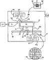
例示のリソグラフィ投影装置は真空チャンバVCを備え、この中で、マスクMAにビームPBが入射し、そして次に基板Wの目標部分に入射する。いわゆる「計測フレーム」MFは装置の主構造と機械的に隔離した、隔離基準フレームを提供する。計測フレームは、低弾性係数を有する、弾性のある支持を可能にするエアマウント(図示せず)により支持された、例えば重量テーブルとして具体化される。基準フレームMFは干渉計IFや他の位置センサといったようなデリケートな構成要素を支持し、それらに振動が及ばないようにする。 The exemplary lithographic projection apparatus comprises a vacuum chamber VC, in which the beam PB is incident on the mask MA and then on a target portion of the substrate W. The so-called "measuring frame" MF provides an isolated reference frame, mechanically isolated from the main structure of the device. The measuring frame is embodied, for example, as a weight table, supported by an air mount (not shown), which has a low elastic modulus and allows elastic support. The reference frame MF supports delicate components, such as the interferometer IF and other position sensors, and keeps them out of vibration.
投影レンズPLは、弾性要素12および支持11により計測フレームMF上に支持されている。投影レンズPLは、計測フレームMF上にそれ自身の支持14を有するシールド構造10にて部分的に囲まれており、熱伝達流体の供給パイプ16と、熱伝達液体のアブダクションパイプ18とに連結されている。
The projection lens PL is supported on the measurement frame MF by the elastic element 12 and the
図2は、投影レンズPLおよびそのシールド構造の実施例をより詳細に示したものである。投影レンズPLは、複数の光学活性ミラー20(1つのミラーのみに参照符号20を付す)および支持構造26を含む。ミラー20はマスクMAを基板W上に結像するように配列されている。ミラーおよび支持構造は望ましくは、Zerodur(登録商標)もしくはULE(登録商標)(超低膨張)ガラスといったような低膨張係数を有するガラス製である。アンバーもまた支持構造26に使用され得る。
FIG. 2 shows an embodiment of the projection lens PL and its shield structure in more detail. The projection lens PL includes a plurality of optically active mirrors 20 (only one mirror is denoted by reference numeral 20) and a
支持構造26は、ミラー20を取り付けるレッグを備えるとともに、ミラー20が配置され、かつ、実質的には投影ビームが通過する開口部分を除いて、ミラー20をほとんど囲んだボックスを備えていることが分かる。代替的にはケージの使用が可能である。ミラーを配したこのボックスあるいはケージ全体は計測フレームMFにより支持される。
The
シールド構造にはミラーシールド22(1つのみに参照符号を付す)、アウターシールド28、およびインナーシールド29を含む。図1において理解されるように、ミラー20および支持構造26とミラーシールド22、アウターシールド28およびインナーシールド19とはこれら各々は計測フレームMF上にそれ自身の支持を有する。ミラーシールド22、アウターシールド28、およびインナーシールド19は計測フレームMF上に結合した支持を有するか、もしくは別々の支持が使用される。または、特にシールド用の支持は、真空チャンバVCに連結されるか、もしくは計測フレーム以外のベースフレーム(図示せず)に連結される。支持構造16は弾性要素12により支持され、計測フレームMFの振動が支持構造に及ばないようにする。簡潔化のため、1つのみの弾性要素12を示しているが、支持構造16は同時に複数のそうした要素により支持されることが理解されよう。同様に、シールド28、29、22は計測フレーム上の一点以上のポイントにて支持され、これらの全部は、弾性要素エレメント12、あるいは支持構造26を支持する他の弾性要素によっては支持されていない。
The shield structure includes a mirror shield 22 (only one is denoted by a reference number), an
図2aは投影システムの詳細を示しており、ミラーシールド22とは隔離した、支持構造26とミラー20との機械的連結200を図示したものである。好ましくは、ミラーシールド22はインナーシールド29への支持連結202を有しているか、あるいはミラーシールド22は別々に支持される。
FIG. 2 a shows details of the projection system, illustrating the
ミラー20各々にそれぞれのミラーシールド22が配設される。各ミラーシールド22は、投影ビームPBを反射するミラー20の面と、支持構造26にミラー20を支持する連結部分を除いて、ミラー20のほぼ全体をしっかり囲む。ミラーシールド22の正確な幾何学的配置は重要ではないが、しかし、この配置は好ましくは、ミラーシールド22により遮断される熱放射の大部分がミラー20への、あるいはミラー20からの熱放射であって、他の構造間の熱放射ではないように形成される。好ましくは、ミラーシールドは、投影ビームPBを反射するミラー20の一部分からの熱放射を除いて、ミラー20への、またはミラー20からの熱放射の大部分(例えば>50%)を遮断するように調整される。
Each
図4は、ミラーシールド22の様々な構成を示しており、ミラー20の背面40のみを覆ったもの、ミラー20の形状に沿ってサイド42を覆ったもの、そして、投影ビームPBにより照射されない前面44の部分をも覆ったものを図示している。後者の構成は、他の構成によるヒーティングや、他の構造のヒーティングを出来るかぎり防止するのに望ましい。
FIG. 4 shows various configurations of the
好ましくは、熱輸送パイプ24がミラーシールド22に取り付けられる。アウターシールド28はミラー20と反対方向を向いた支持構造26の面に近接して設けられており、インナーシールド29はミラー20に面した支持構造の面に近接して設けられている。好ましくは、熱輸送パイプ27がアウターシールド28とインナーシールド29の両方に配設される。熱輸送パイプ24、27は直列に配列されるか、もしくは並列に配列される。
Preferably, a
図5は別の実施例を示したものであり、熱シールド52はミラー50の面への平均垂線方向に沿って伸長する。このようにして、ミラー50の反射面から反射された放射線のその少なくともいくらかは冷却された熱シールド52によって遮断される。好ましくは、熱シールドは投影ビームPBを遮ることなく出来るだけ長く(一般的には少なくともミラー50の直径の1/2)延在する。一般に、シールド52は垂線で囲む円柱形でありミラーを通る平面で円柱の断面のみを示している。ミラーが図のように示されているが、代わりに平行面シールドを使用することも可能である。
FIG. 5 shows another embodiment, in which the
稼動時に投影ビームPBはマスクMAに投影される。マスクMAはミラー20の光学動作により基板W上に結像される。熱伝達流体は熱伝達パイプ24、27によって送り込まれる。例示の方法により、水が熱伝達流体として使用され得る。
In operation, the projection beam PB is projected onto the mask MA. The mask MA is imaged on the substrate W by the optical operation of the
ミラーシールド22はミラー20の温度の揺れを制限する役割を有する。必然的に投影ビームPBがミラー20より反射されると吸収がいくらかおきる。この吸収がミラー20、マスクMA、および基板W間の幾何学的関係に影響を及ぼすと、結像問題が生じる。サブミクロンの精度が要求される場合、非常に小さな障害がすでにダメージとなり得る。これは、例えばEIVビームといったような短波長のビームPBで特に問題となる。なぜならば、こうしたビームは高い真空度を必要とし(吸収熱を減じるのを困難にする)、比較的高い吸収を伴うからである。
The
ミラーシールド22はミラー20から放射された熱を吸収する。過剰な熱は熱輸送パイプ24を介し取り除かれる。こうして、ミラー20のヒーティングによる影響が減じられ、ミラー20の温度はミラーシールドにより、熱輸送流体により決定されるような熱平衡に近づけられる。ミラーシールド22をミラー20の周りにしっかりと配備することにより、最少のシールド材料にて最大の熱が吸収され、ミラー20に到達する他のソースからの熱放射はわずかとなる。よって、ミラーシールド22に対する熱輸送能力は小さくて十分である。ミラーシールド22はミラー20とは別々に計測フレームMFに支持されているため、熱輸送流体による機械的振動がミラーの位置に影響を与えることはそれほどない。加えて、ミラーシールド22は他の構造からの放射熱によるミラー20のヒーティングを防止する。
The
好ましくは、ミラーシールド22の表面は、ミラー20にきっちり面した内表面の熱放射吸収係数が、ミラー20に直には面していない外表面の熱放射吸収係数よりも高くなるように処理される。アルミニウムを研磨することによって、例えば吸収係数を0.05まで低くすることが可能であり、同様の効果はゴールド層のコーティングによっても達せられる。酸化アルミニウムといったようなセラミック層でのコーティングにより、吸収係数を0.8乃至0.9にすることが可能である。本発明は、吸収に影響を与えるこうした方法を制限するものではないことは明らかである。あらゆる既知の技術が使用され得る。内表面の吸収係数はおおよそ0.8、乃至は0.9をも超過するほど出来るだけ高い方が好ましく、これに対し、外表面の吸収係数はおおよそ0.2乃至は0.1をも下回るほど出来るだけ低いほうが好ましい。結果として、他の構造からのヒーティングを防止するために、ミラーシールド22に最小限の熱伝播を必要とする。
Preferably, the surface of the
支持構造26のアウターシールド28は、ヒーティングによる支持構造26の幾何学的変形を防ぐ役割を果たす。アウターシールド28は支持構造26の低減温度のレベルに維持する。支持構造26の温度は、熱伝達流体により決定されるようなアウターシールド28との、熱平衡をほぼもたらすようにされる。よって、支持構造26の変形による投影レンズの幾何学的変形が実質的に回避される。加えて、アウターシールド28は外部熱源からの放射線による支持構造26のヒーティングを防止する。
The
好ましくは、アウターシールド28は、支持構造26の外表面への、またはこの外表面からの熱放射の大部分を遮断するように成形、かつ配置され、それにより、遮られた放射線の少量にしかすぎない部分(例えば<10%)は支持構造26への、あるいは支持構造26からのものではないようにする。望ましいどのようなシールド幾何学的アレンジメントであってもこの目的に使用され得る。
Preferably, the
好ましくは、ミラーシールド28の表面は、支持構造26に面した内表面の熱放射吸収係数が、支持構造26に直には面していない外表面の熱放射吸収係数よりも高くなるように処理される。内表面の吸収係数はおおよそ0.8、乃至は0.9をも超過するほど出来るだけ高い方が好ましく、これに対し、外表面の吸収係数はおおよそ0.2乃至は0.1をも下回るほど出来るだけ低いほうが好ましい。結果として、他の構造からのヒーティングを防ぐために、アウターシールド28に最小限の熱伝達を必要とする。
Preferably, the surface of the
支持構造26のインナーシールド29は、ミラー20の露出表面からの放射線と、支持構造26の孔(高い真空度を可能にするため大きな孔が設けられなくてはならない)から「可視」の外部熱源からの放射線によるヒーティングとによって生じる支持構造26の幾何学的変形を防ぐ役割を果たす。インナーシールド29は支持構造26の温度を減じたレベルに維持する。支持構造26の温度はインナーシールド29により、熱伝達流体により決定されるような熱平衡をほぼもたらすようにされる。好ましくは、インナーシールド29表面は、支持構造26にきっちりと面した内表面の熱放射吸収係数が、支持構造26に直には面していない外表面の熱放射吸収係数よりも高くなるように処理される。内表面の吸収係数は、おおよそ0.8、乃至は0.9をも超過するほど出来るだけ高い方が好ましく、これに対し、外表面の吸収係数はおおよそ0.2乃至は0.1をも下回るほど出来るだけ低いほうが望ましい。結果的に、他の構造からのヒーティングを防止するために、インナーシールド29に最小限の熱伝達を必要とする。
The
ミラーの位置調整のために、支持構造26とミラー20間にアクチュエータとセンサ(図示せず)を配設することが出来る。この場合、ミラーシールド22はこうしたアクチュエータおよびセンサからの放射線からミラー20を保護する役割を有する。インナーシールド29は、支持構造26と、これらアクチュエータ、センサ間に入り、アクチュエータおよびセンサによる熱放射から支持構造を保護するように配置されることが望ましい。
An actuator and a sensor (not shown) can be disposed between the
ミラーシールド22、アウターシールド28、およびインナーシールド29の使用法を最適な結合効果を達成するように共に記載を行ったが、これらのシールドのいずれかを使用せずに、1つずつ、もしくは組み合わせてこうしたシールドを使用することも可能であることを理解されたい。例えば、ヒーティングの主原因が、支持構造26の外表面に放射する外部熱源からのものである場合、アウターシールド28のみで十分である。この場合、ミラーシールド22は投影ビームPBによる熱問題が生じた際に追加的に使用される。また他の例として、ヒーティングの主原因が投影ビームPBである場合、ミラーシールド22このままのみで十分であり、状況によってはインナーシールド29が支持構造26を保護するために追加される。
The use of the
同様に、例えば、スペース制限によって少ない冷却効果を有するシールド22、28、29上の箇所において吸収を少なくするか、もしくは、ミラー20といったような熱源から、ミラー20あるいはそのミラーシールド22といったような温度にデリケートな構成要素への反射の経路にある箇所にて高い吸収をもたらすといったように、吸収係数を局所的に変えることが可能である。
Similarly, for example, the absorption on the
「熱伝達」という用語を、流体およびパイプ24、27全体にわたり使用したが、アブダクションパイプ18により過剰な熱を取り除くことにより、たいていの状況下でパイプ24、27は冷却パイプの役割を果たし、流体は冷却流体の役割を果たすことを理解されたい。しかし、投影ビームがないとき、本発明を逸脱することなく、流体が、ミラー20および支持構造を通常よりも高い温度に維持するために使用され得る。この場合、熱は通常通りミラー20に伝わるが、例えば投影ビームによって、より多くの熱がミラーに与えられると、この伝わる熱の量は減じられる。
Although the term "heat transfer" has been used throughout the fluid and the
図3は、ミラー20および/または支持構造26の温度を調整するために制御ループが使用される別の実施形態を示したものである。この実施例において、1つ以上のセンサ30(例えば温度依存抵抗)が1つあるいは複数のミラーシールド22に配備される。また、ヒータ32が熱輸送流体の供給パイプに連結して設けられる。制御回路34がセンサ30およびヒータ32間に連結され、ヒーティングの量を調整するようにアレンジされることにより、平均感知温度が設定温度に対して調整される。また、循環ポンプ36が供給パイプに設けられる。図中示していないが、流体からの過剰な熱を取り除くために、ヒータ32の上流に冷却要素が配備される。
FIG. 3 illustrates another embodiment in which a control loop is used to regulate the temperature of
原理的に、共通ヒータ32が全ミラー20および支持構造26のための流体を加熱するために設けられる。この場合、いくつかのセンサが異なる熱シールドに設けられ、平均感知温度が調整される。しかし、実施例においては、各ヒータ32が流体の流路の異なる平行部に配設されることにより、ミラー各々の、もしくはミラー群各々の温度を別々に調整する。この各々は、その該当するミラーもしくは複数のミラーの温度を感知するセンサに反応する。
In principle, a
しかし、本発明はこの方法における温度調整に限定されるものではないことを理解されたい。多くのケースではおそらく流体温度を一定に保つ以外では、温度調整がともに省かれるであろう。また、本発明から逸脱することなく、ミラー20、あるいは支持構造26にセンサ30を設けるか、もしくはミラーシールド22、支持構造26および/またはミラー20の両方にセンサを設けることも可能である。熱シールドにセンサを配設することにより、ミラー20の機械的な障害を最小限に抑える。流体は加熱されるかわりに、調整される量により冷却され得る。冷却あるいは加熱の量を調整する代わりに、温度調整のために流体の流量が調整され得る。
However, it should be understood that the invention is not limited to temperature regulation in this way. In many cases, temperature regulation will probably be omitted altogether, except to keep the fluid temperature constant. It is also possible to provide the
本発明は、パイプを循環する流体(「流体」なる用語は、液体、気体、ガス、およびこれら混合の両方を網羅する)を使用する流体冷却を用いる実施例に関して詳細説明を行ったが、ヒート・パイプといったような、熱シールドへの/からの熱を伝えるアクティブ冷却の他の形態も含まれることを理解されたい。 Although the present invention has been described in detail with respect to embodiments employing fluid cooling using fluid circulating through the pipe (the term "fluid" covers both liquids, gases, gases and mixtures thereof), -It should be understood that other forms of active cooling that conduct heat to / from the heat shield, such as pipes, are also included.
さらに、冷却流体が往復する循環流路を示したが、本文に使用した「熱伝達回路」は流体の循環を必要とするものでないことを理解されたい。循環流体の代わりに、新鮮な流体を使用することも可能である。 Further, while a circulation path through which the cooling fluid reciprocates is shown, it should be understood that the "heat transfer circuit" used herein does not require circulation of the fluid. Instead of a circulating fluid, it is also possible to use fresh fluid.
以上、本発明の実施形態を詳細に説明したが、本発明の範囲を逸脱することなく他の方法でも具体化できることは当業者にとって明らかである。本詳細説明は本発明を制限する意図ではない。 Although the embodiments of the present invention have been described in detail, it will be apparent to those skilled in the art that other methods can be embodied without departing from the scope of the present invention. This detailed description is not intended to limit the invention.
Claims (16)
− 所望するパターンに従って投影ビームをパターン化するパターニング手段を支持する支持装置と、
− 基板を保持する基板テーブルと、
− 光学活性ミラー、少なくともミラーを支持する支持構造、および、支持構造および/またはミラーの表面への、あるいは支持構造および/またはミラーの表面からの熱放射を遮断するように配置された少なくとも1つの熱放射シールドとによって構成されている、パターン化されたビームを基板の目標部分に投影する投影システムと、
− 少なくとも1つの熱シールドへの、あるいは少なくとも1つの熱シールドからの熱伝達を行う、少なくとも1つの熱シールドと熱的接触を行った熱伝達回路と、
− 支持構造および少なくとも1つの放射熱シールドをそれぞれ支持フレームに支持するために、それぞれ別々の支持要素を有した支持フレームとから成るリソグラフィ投影装置において、ミラーの支持要素と、少なくとも1つの熱シールドは、支持フレームによる支持を除き、互いに機械的に連結を行っていないことを特徴とするリソグラフィ投影装置。 A radiation system for providing a projection beam of radiation;
A support device for supporting a patterning means for patterning the projection beam according to a desired pattern;
A substrate table for holding the substrate;
An optically active mirror, a support structure supporting at least the mirror, and at least one arranged to block thermal radiation to or from the surface of the support structure and / or the mirror; A projection system configured to project the patterned beam onto a target portion of the substrate, the projection system comprising a thermal radiation shield;
-A heat transfer circuit in thermal contact with at least one heat shield for transferring heat to or from at least one heat shield;
A lithographic projection apparatus comprising a support frame and a support frame having separate support elements for supporting the support structure and the at least one radiant heat shield respectively on the support frame, wherein the support element of the mirror and the at least one heat shield are A lithographic projection apparatus characterized in that the lithographic projection apparatus is not mechanically connected to each other except for support by a support frame.
− 放射線システムを用いて放射線の投影ビームを供給するステップと、
− パターニング手段を用いて投影ビームのその断面にパターンを与えるステップと、
− 光学活性ミラーにより、放射線感光材料の層の目標部分に放射線のパターン化されたビームを投影するステップと、
− ミラーおよびその支持構造は全体として熱シールドとは別に支持されており、少なくとも1つの熱シールドにより、光学動作ミラーおよび/または光学動作ミラーの支持構造への、あるいは光学動作ミラーおよび/または光学動作ミラーの支持構造からの熱放射をシールドするステップと、
− 少なくとも1つの熱シールドに機械的に取り付けられたパイプを通して少なくとも1つの熱シールドに熱伝達流体を供給するステップとから成るデバイス製造方法。 Providing a substrate at least partially covered by a layer of radiation-sensitive material;
Providing a projection beam of radiation using a radiation system;
-Applying a pattern to that cross section of the projection beam using patterning means;
Projecting a patterned beam of radiation onto a target portion of the layer of radiation-sensitive material by an optically active mirror;
The mirror and its supporting structure are supported as a whole separately from the heat shield, and the at least one heat shield allows the optical working mirror and / or the supporting structure of the optical working mirror or to the optical working mirror and / or the optical operation; Shielding heat radiation from the mirror support structure;
Supplying the heat transfer fluid to the at least one heat shield through a pipe mechanically attached to the at least one heat shield.
− 所望するパターンに従って投影ビームをパターン化するパターニング手段を支持する支持構造と、
− 基板を保持する基板テーブルと、
− 光学動作ミラー、少なくともミラーを支持する支持構造、および、支持構造および/またはミラーの外表面への、あるいは支持構造および/またはミラーの外表面からの熱放射を遮断するように配置された、ミラーと反対方向を向く支持構造の外表面に近接したアウターシールドとによって構成されている、パターン化されたビームを基板の目標部分に投影する投影システムとから成ることを特徴とするリソグラフィ投影装置。 A radiation system for providing a projection beam of radiation;
A support structure for supporting patterning means for patterning the projection beam according to a desired pattern;
A substrate table for holding the substrate;
-An optically operating mirror, at least a support structure supporting the mirror, and arranged to block thermal radiation to or from the outer surface of the support structure and / or the mirror; A lithographic projection apparatus, comprising: a projection system configured to project a patterned beam onto a target portion of a substrate, the projection system comprising a mirror and an outer shield proximate an outer surface of a support structure facing in an opposite direction.
Applications Claiming Priority (1)
| Application Number | Priority Date | Filing Date | Title |
|---|---|---|---|
| EP03076433A EP1477850A1 (en) | 2003-05-13 | 2003-05-13 | Lithographic apparatus and device manufacturing method |
Publications (2)
| Publication Number | Publication Date |
|---|---|
| JP2004343116A true JP2004343116A (en) | 2004-12-02 |
| JP3929993B2 JP3929993B2 (en) | 2007-06-13 |
Family
ID=33016938
Family Applications (1)
| Application Number | Title | Priority Date | Filing Date |
|---|---|---|---|
| JP2004142232A Expired - Fee Related JP3929993B2 (en) | 2003-05-13 | 2004-05-12 | Lithographic apparatus, device manufacturing method, and device manufactured thereby |
Country Status (7)
| Country | Link |
|---|---|
| US (1) | US7116399B2 (en) |
| EP (2) | EP1477850A1 (en) |
| JP (1) | JP3929993B2 (en) |
| KR (1) | KR100654418B1 (en) |
| CN (1) | CN100422855C (en) |
| SG (1) | SG115684A1 (en) |
| TW (1) | TWI256075B (en) |
Cited By (12)
| Publication number | Priority date | Publication date | Assignee | Title |
|---|---|---|---|---|
| JP2006173618A (en) * | 2004-12-15 | 2006-06-29 | Asml Netherlands Bv | Lithography equipment |
| JP2007180551A (en) * | 2005-12-28 | 2007-07-12 | Asml Netherlands Bv | Lithographic apparatus, system, and method for manufacturing device |
| JP2011512018A (en) * | 2007-10-09 | 2011-04-14 | カール・ツァイス・エスエムティー・ゲーエムベーハー | Optical element temperature control device |
| KR20110046527A (en) * | 2008-08-11 | 2011-05-04 | 칼 짜이스 에스엠테 게엠베하 | Low contamination optical array |
| JP2012522257A (en) * | 2009-03-27 | 2012-09-20 | カール・ツァイス・エスエムティー・ゲーエムベーハー | Optical assembly |
| JP2013506978A (en) * | 2009-09-30 | 2013-02-28 | カール・ツァイス・エスエムティー・ゲーエムベーハー | Optical structure of a microlithographic projection exposure apparatus |
| JP2014526792A (en) * | 2012-03-05 | 2014-10-06 | カール・ツァイス・エスエムティー・ゲーエムベーハー | Optical imaging apparatus having vibration isolation support unit |
| JP2017526010A (en) * | 2014-08-21 | 2017-09-07 | カール・ツァイス・エスエムティー・ゲーエムベーハー | Mirror module especially for microlithography projection exposure equipment |
| JP2017538164A (en) * | 2014-12-03 | 2017-12-21 | カール・ツァイス・エスエムティー・ゲーエムベーハー | Optical assembly having heat conducting components |
| JP2020506432A (en) * | 2017-02-07 | 2020-02-27 | レイセオン カンパニー | Total reflection solar coronagraph sensor and thermal control subsystem |
| JP2020115237A (en) * | 2005-12-30 | 2020-07-30 | エーエスエムエル ネザーランズ ビー.ブイ. | Lithographic apparatus and device manufacturing method |
| JP2021515907A (en) * | 2018-03-06 | 2021-06-24 | エーエスエムエル ネザーランズ ビー.ブイ. | Radiation shielding devices and devices with such shielding devices |
Families Citing this family (19)
| Publication number | Priority date | Publication date | Assignee | Title |
|---|---|---|---|---|
| EP1513017A1 (en) * | 2003-09-04 | 2005-03-09 | ASML Netherlands B.V. | Lithographic apparatus and device manufacturing method |
| US6977713B2 (en) * | 2003-12-08 | 2005-12-20 | Asml Netherlands B.V. | Lithographic apparatus and device manufacturing method |
| WO2009039883A1 (en) * | 2007-09-26 | 2009-04-02 | Carl Zeiss Smt Ag | Optical imaging device with thermal stabilization |
| US9410010B2 (en) | 2007-12-10 | 2016-08-09 | E I Du Pont De Nemours And Company | Urea-terminated polyurethane dispersants |
| US20130022746A9 (en) * | 2007-12-10 | 2013-01-24 | Harry Joseph Spinelli | Aqueous inkjet inks with ionically stabilized dispersions and polyurethane ink additives |
| US20090259012A1 (en) * | 2007-12-10 | 2009-10-15 | Roberts C Chad | Urea-terminated ether polyurethanes and aqueous dispersions thereof |
| WO2009143441A1 (en) * | 2008-05-23 | 2009-11-26 | E. I. Du Pont De Nemours And Company | Urea-terminated polyurethane dispersants |
| US20110060102A1 (en) * | 2008-05-23 | 2011-03-10 | E.I. Du Pont De Nemours And Company | Urea-terminated polyurethane dispersants |
| WO2009143418A1 (en) * | 2008-05-23 | 2009-11-26 | E. I. Du Pont De Nemours And Company | Inkjet ink with self dispersed pigments and polyurethane ink additives |
| CN102216804B (en) * | 2008-09-23 | 2013-12-04 | 涅磐公司 | Deicing system in sodar systems |
| JP5495547B2 (en) * | 2008-12-25 | 2014-05-21 | キヤノン株式会社 | Processing apparatus and device manufacturing method |
| DE102009045193A1 (en) | 2009-09-30 | 2011-04-14 | Carl Zeiss Smt Gmbh | Optical arrangement in an optical system, in particular in a microlithographic projection exposure apparatus |
| DE102009045223A1 (en) * | 2009-09-30 | 2011-03-31 | Carl Zeiss Smt Gmbh | Optical arrangement in a projection exposure machine for EUV lithography |
| KR101895083B1 (en) * | 2010-07-30 | 2018-10-18 | 칼 짜이스 에스엠티 게엠베하 | Euv exposure apparatus |
| EP2726939B1 (en) | 2011-07-01 | 2020-09-16 | Carl Zeiss SMT GmbH | Optical imaging arrangement with individually actively supported components |
| CN103364077B (en) * | 2012-03-28 | 2016-06-29 | 睿励科学仪器(上海)有限公司 | For the temperature-controlled process of optical gauge and equipment and optical gauge |
| US9658542B2 (en) | 2013-10-14 | 2017-05-23 | Carl Zeiss Smt Gmbh | Optical element |
| DE102018200539A1 (en) * | 2018-01-15 | 2019-07-18 | Carl Zeiss Smt Gmbh | Projection exposure apparatus for semiconductor lithography with heat shielding elements |
| DE102023203872A1 (en) | 2023-04-26 | 2024-03-28 | Carl Zeiss Smt Gmbh | Assembly for an optical system |
Family Cites Families (16)
| Publication number | Priority date | Publication date | Assignee | Title |
|---|---|---|---|---|
| US6714278B2 (en) * | 1996-11-25 | 2004-03-30 | Nikon Corporation | Exposure apparatus |
| JPH10209040A (en) * | 1996-11-25 | 1998-08-07 | Nikon Corp | Aligner |
| US6118599A (en) * | 1998-11-03 | 2000-09-12 | Nikon Corporation | Hybrid optical barrel |
| JP2002118058A (en) * | 2000-01-13 | 2002-04-19 | Nikon Corp | Projection aligner and projection exposure method |
| US6621557B2 (en) * | 2000-01-13 | 2003-09-16 | Nikon Corporation | Projection exposure apparatus and exposure methods |
| JP4809987B2 (en) * | 2000-03-30 | 2011-11-09 | キヤノン株式会社 | Support structure for optical element, exposure apparatus using the same, and method for manufacturing semiconductor device |
| US6630984B2 (en) * | 2000-08-03 | 2003-10-07 | Asml Netherlands B.V. | Lithographic apparatus, device manufacturing method, and device manufactured thereby |
| EP1178357A1 (en) * | 2000-08-03 | 2002-02-06 | Asm Lithography B.V. | Lithographic apparatus |
| DE10106605A1 (en) * | 2001-02-13 | 2002-08-22 | Zeiss Carl | System for eliminating or at least damping vibrations |
| DE10134387A1 (en) * | 2001-07-14 | 2003-01-23 | Zeiss Carl | Optical system with several optical elements |
| JP2003234276A (en) * | 2002-02-07 | 2003-08-22 | Nikon Corp | Exposure device and optical device, manufacturing method of device |
| EP1376239A3 (en) * | 2002-06-25 | 2005-06-29 | Nikon Corporation | Cooling device for an optical element |
| JP2004029314A (en) | 2002-06-25 | 2004-01-29 | Nikon Corp | Device for cooling optical element, method of cooling optical element and exposure device |
| EP1387054B1 (en) * | 2002-07-31 | 2012-07-25 | Canon Kabushiki Kaisha | Cooling apparatus for an optical element, exposure apparatus comprising said cooling apparatus, and device fabrication method |
| JP2004080025A (en) | 2002-07-31 | 2004-03-11 | Canon Inc | Cooling device and method therefor, and aligner therewith |
| US6992306B2 (en) * | 2003-04-15 | 2006-01-31 | Canon Kabushiki Kaisha | Temperature adjustment apparatus, exposure apparatus having the same, and device fabricating method |
-
2003
- 2003-05-13 EP EP03076433A patent/EP1477850A1/en not_active Withdrawn
-
2004
- 2004-05-06 SG SG200402416A patent/SG115684A1/en unknown
- 2004-05-12 EP EP04076407A patent/EP1477855B1/en not_active Not-in-force
- 2004-05-12 JP JP2004142232A patent/JP3929993B2/en not_active Expired - Fee Related
- 2004-05-12 CN CNB2004100595085A patent/CN100422855C/en active Active
- 2004-05-12 TW TW093113357A patent/TWI256075B/en active
- 2004-05-13 US US10/844,570 patent/US7116399B2/en active Active
- 2004-05-13 KR KR1020040033773A patent/KR100654418B1/en active IP Right Grant
Cited By (30)
| Publication number | Priority date | Publication date | Assignee | Title |
|---|---|---|---|---|
| JP4621584B2 (en) * | 2004-12-15 | 2011-01-26 | エーエスエムエル ネザーランズ ビー.ブイ. | Lithographic apparatus |
| JP2006173618A (en) * | 2004-12-15 | 2006-06-29 | Asml Netherlands Bv | Lithography equipment |
| JP2007180551A (en) * | 2005-12-28 | 2007-07-12 | Asml Netherlands Bv | Lithographic apparatus, system, and method for manufacturing device |
| JP4546446B2 (en) * | 2005-12-28 | 2010-09-15 | エーエスエムエル ネザーランズ ビー.ブイ. | Lithographic apparatus, system and device manufacturing method |
| JP7193499B2 (en) | 2005-12-30 | 2022-12-20 | エーエスエムエル ネザーランズ ビー.ブイ. | Lithographic apparatus and device manufacturing method |
| JP2020115237A (en) * | 2005-12-30 | 2020-07-30 | エーエスエムエル ネザーランズ ビー.ブイ. | Lithographic apparatus and device manufacturing method |
| US11275316B2 (en) | 2005-12-30 | 2022-03-15 | Asml Netherlands B.V. | Lithographic apparatus and device manufacturing method |
| US11669021B2 (en) | 2005-12-30 | 2023-06-06 | Asml Netherlands B.V. | Lithographic apparatus and device manufacturing method |
| JP2011512018A (en) * | 2007-10-09 | 2011-04-14 | カール・ツァイス・エスエムティー・ゲーエムベーハー | Optical element temperature control device |
| US8328374B2 (en) | 2007-10-09 | 2012-12-11 | Carl Zeiss Smt Gmbh | Device for controlling temperature of an optical element |
| US8632194B2 (en) | 2007-10-09 | 2014-01-21 | Carl Zeiss Smt Gmbh | Device for controlling temperature of an optical element |
| JP2014179624A (en) * | 2007-10-09 | 2014-09-25 | Carl Zeiss Smt Gmbh | Temperature control device of optical element |
| US8894225B2 (en) | 2007-10-09 | 2014-11-25 | Carl Zeiss Smt Gmbh | Device for controlling temperature of an optical element |
| US9195151B2 (en) | 2007-10-09 | 2015-11-24 | Carl Zeiss Smt Gmbh | Device for controlling temperature of an optical element |
| US9442397B2 (en) | 2007-10-09 | 2016-09-13 | Carl Zeiss Smt Gmbh | Device for controlling temperature of an optical element |
| JP2011530820A (en) * | 2008-08-11 | 2011-12-22 | カール・ツァイス・エスエムティー・ゲーエムベーハー | Low contamination optical device |
| KR20110046527A (en) * | 2008-08-11 | 2011-05-04 | 칼 짜이스 에스엠테 게엠베하 | Low contamination optical array |
| KR101645750B1 (en) | 2008-08-11 | 2016-08-04 | 칼 짜이스 에스엠테 게엠베하 | Low-contamination optical arrangement |
| US8964162B2 (en) | 2009-03-27 | 2015-02-24 | Carl Zeiss Smt Gmbh | Optical assembly |
| JP2012522257A (en) * | 2009-03-27 | 2012-09-20 | カール・ツァイス・エスエムティー・ゲーエムベーハー | Optical assembly |
| US9436101B2 (en) | 2009-09-30 | 2016-09-06 | Carl Zeiss Smt Gmbh | Optical arrangement and microlithographic projection exposure apparatus including same |
| JP2013506978A (en) * | 2009-09-30 | 2013-02-28 | カール・ツァイス・エスエムティー・ゲーエムベーハー | Optical structure of a microlithographic projection exposure apparatus |
| JP2014526792A (en) * | 2012-03-05 | 2014-10-06 | カール・ツァイス・エスエムティー・ゲーエムベーハー | Optical imaging apparatus having vibration isolation support unit |
| JP2017526010A (en) * | 2014-08-21 | 2017-09-07 | カール・ツァイス・エスエムティー・ゲーエムベーハー | Mirror module especially for microlithography projection exposure equipment |
| JP2017538164A (en) * | 2014-12-03 | 2017-12-21 | カール・ツァイス・エスエムティー・ゲーエムベーハー | Optical assembly having heat conducting components |
| US10509336B2 (en) | 2014-12-03 | 2019-12-17 | Carl Zeiss Smt Gmbh | Optical assembly having a thermally conductive component |
| US11194119B2 (en) | 2014-12-03 | 2021-12-07 | Carl Zeiss Smt Gmbh | Optical assembly having a thermally conductive component |
| JP2020506432A (en) * | 2017-02-07 | 2020-02-27 | レイセオン カンパニー | Total reflection solar coronagraph sensor and thermal control subsystem |
| JP2021515907A (en) * | 2018-03-06 | 2021-06-24 | エーエスエムエル ネザーランズ ビー.ブイ. | Radiation shielding devices and devices with such shielding devices |
| JP7402808B2 (en) | 2018-03-06 | 2023-12-21 | エーエスエムエル ネザーランズ ビー.ブイ. | Radiation shielding devices and equipment equipped with such shielding devices |
Also Published As
| Publication number | Publication date |
|---|---|
| TWI256075B (en) | 2006-06-01 |
| US20050018154A1 (en) | 2005-01-27 |
| US7116399B2 (en) | 2006-10-03 |
| CN100422855C (en) | 2008-10-01 |
| JP3929993B2 (en) | 2007-06-13 |
| TW200510950A (en) | 2005-03-16 |
| KR20040097950A (en) | 2004-11-18 |
| EP1477855A1 (en) | 2004-11-17 |
| KR100654418B1 (en) | 2006-12-05 |
| EP1477850A1 (en) | 2004-11-17 |
| CN1550909A (en) | 2004-12-01 |
| SG115684A1 (en) | 2005-10-28 |
| EP1477855B1 (en) | 2012-01-11 |
Similar Documents
| Publication | Publication Date | Title |
|---|---|---|
| JP3929993B2 (en) | Lithographic apparatus, device manufacturing method, and device manufactured thereby | |
| EP1653283B1 (en) | Lithographic apparatus and device manufacturing method | |
| US20050206863A1 (en) | Lithographic apparatus, device manufacturing method, and device manufactured thereby | |
| KR100665750B1 (en) | Lithographic Apparatus and Device Manufacturing Method | |
| KR100748446B1 (en) | Lithographic apparatus comprising a gas flushing system | |
| US7375794B2 (en) | Lithographic apparatus and device manufacturing method | |
| JP4166730B2 (en) | Lithographic projection apparatus and device manufacturing method | |
| US7889321B2 (en) | Illumination system for illuminating a patterning device and method for manufacturing an illumination system | |
| US20050105066A1 (en) | Lithographic apparatus and device manufacturing method | |
| KR100700368B1 (en) | Lithographic Apparatus and Device Manufacturing Method | |
| JP2005175490A (en) | Lithography system, and device manufacturing method | |
| EP1178357A1 (en) | Lithographic apparatus | |
| US7471373B2 (en) | Lithographic apparatus with patterning device position determination | |
| JP2006073895A (en) | Cooling device, aligner, and device manufacturing method | |
| US20100103390A1 (en) | Lithographic apparatus and device manufacturing method | |
| JP2004274024A (en) | Lithographic apparatus, device manufacturing method, and device manufactured thereby | |
| KR20100100921A (en) | A lithographic apparatus, a projection system and a device manufacturing method |
Legal Events
| Date | Code | Title | Description |
|---|---|---|---|
| A977 | Report on retrieval |
Free format text: JAPANESE INTERMEDIATE CODE: A971007 Effective date: 20050725 |
|
| A131 | Notification of reasons for refusal |
Free format text: JAPANESE INTERMEDIATE CODE: A131 Effective date: 20050729 |
|
| A601 | Written request for extension of time |
Free format text: JAPANESE INTERMEDIATE CODE: A601 Effective date: 20051031 |
|
| A602 | Written permission of extension of time |
Free format text: JAPANESE INTERMEDIATE CODE: A602 Effective date: 20051104 |
|
| A521 | Written amendment |
Free format text: JAPANESE INTERMEDIATE CODE: A523 Effective date: 20060123 |
|
| RD03 | Notification of appointment of power of attorney |
Free format text: JAPANESE INTERMEDIATE CODE: A7423 Effective date: 20060904 |
|
| A131 | Notification of reasons for refusal |
Free format text: JAPANESE INTERMEDIATE CODE: A131 Effective date: 20061018 |
|
| A521 | Written amendment |
Free format text: JAPANESE INTERMEDIATE CODE: A523 Effective date: 20070115 |
|
| TRDD | Decision of grant or rejection written | ||
| A01 | Written decision to grant a patent or to grant a registration (utility model) |
Free format text: JAPANESE INTERMEDIATE CODE: A01 Effective date: 20070208 |
|
| A61 | First payment of annual fees (during grant procedure) |
Free format text: JAPANESE INTERMEDIATE CODE: A61 Effective date: 20070307 |
|
| R150 | Certificate of patent or registration of utility model |
Ref document number: 3929993 Country of ref document: JP Free format text: JAPANESE INTERMEDIATE CODE: R150 Free format text: JAPANESE INTERMEDIATE CODE: R150 |
|
| FPAY | Renewal fee payment (event date is renewal date of database) |
Free format text: PAYMENT UNTIL: 20100316 Year of fee payment: 3 |
|
| FPAY | Renewal fee payment (event date is renewal date of database) |
Free format text: PAYMENT UNTIL: 20110316 Year of fee payment: 4 |
|
| R250 | Receipt of annual fees |
Free format text: JAPANESE INTERMEDIATE CODE: R250 |
|
| R250 | Receipt of annual fees |
Free format text: JAPANESE INTERMEDIATE CODE: R250 |
|
| FPAY | Renewal fee payment (event date is renewal date of database) |
Free format text: PAYMENT UNTIL: 20130316 Year of fee payment: 6 |
|
| R250 | Receipt of annual fees |
Free format text: JAPANESE INTERMEDIATE CODE: R250 |
|
| FPAY | Renewal fee payment (event date is renewal date of database) |
Free format text: PAYMENT UNTIL: 20140316 Year of fee payment: 7 |
|
| R250 | Receipt of annual fees |
Free format text: JAPANESE INTERMEDIATE CODE: R250 |
|
| R250 | Receipt of annual fees |
Free format text: JAPANESE INTERMEDIATE CODE: R250 |
|
| R250 | Receipt of annual fees |
Free format text: JAPANESE INTERMEDIATE CODE: R250 |
|
| R250 | Receipt of annual fees |
Free format text: JAPANESE INTERMEDIATE CODE: R250 |
|
| R250 | Receipt of annual fees |
Free format text: JAPANESE INTERMEDIATE CODE: R250 |
|
| R250 | Receipt of annual fees |
Free format text: JAPANESE INTERMEDIATE CODE: R250 |
|
| R250 | Receipt of annual fees |
Free format text: JAPANESE INTERMEDIATE CODE: R250 |
|
| R250 | Receipt of annual fees |
Free format text: JAPANESE INTERMEDIATE CODE: R250 |
|
| LAPS | Cancellation because of no payment of annual fees |