JP2004342123A - Information processor and method and recording medium - Google Patents
Information processor and method and recording medium Download PDFInfo
- Publication number
- JP2004342123A JP2004342123A JP2004188866A JP2004188866A JP2004342123A JP 2004342123 A JP2004342123 A JP 2004342123A JP 2004188866 A JP2004188866 A JP 2004188866A JP 2004188866 A JP2004188866 A JP 2004188866A JP 2004342123 A JP2004342123 A JP 2004342123A
- Authority
- JP
- Japan
- Prior art keywords
- block
- data
- area
- user
- blocks
- Prior art date
- Legal status (The legal status is an assumption and is not a legal conclusion. Google has not performed a legal analysis and makes no representation as to the accuracy of the status listed.)
- Granted
Links
Images


Abstract
Description
本発明は、情報処理装置および情報処理方法、並びに記録媒体に関し、特に、所定の利用者からのコマンドを受信し、そのコマンドを処理し、処理の結果を送信する情報処理装置および情報処理方法、並びに記録媒体に関する。 The present invention relates to an information processing apparatus, an information processing method, and a recording medium, and more particularly, to an information processing apparatus and an information processing method for receiving a command from a predetermined user, processing the command, and transmitting a processing result, And a recording medium.
電子マネーシステムやセキュリティシステムで利用されるICカード(スマートカード)が開発されている。 IC cards (smart cards) used in electronic money systems and security systems have been developed.
このようなICカードは、各種処理を行うCPUや、処理に必要なデータなどを記憶するメモリを内蔵し、所定のリーダ/ライタ(R/W)に接触させた状態で、データの送受信を行っている。 Such an IC card has a built-in CPU for performing various processes and a memory for storing data necessary for the processes, and transmits and receives data while being in contact with a predetermined reader / writer (R / W). ing.
また、ICカードの中には、自らはバッテリを有していないバッテリレス型のICカードもある。このようなバッテリレス型のICカードは、R/Wから電力を供給される。 Further, among IC cards, there is a batteryless IC card which does not have a battery. Such a batteryless IC card is supplied with power from the R / W.
しかしながら、このようなICカードにおいては、R/Wに接触させた状態で使用することを前提としているので、非接触で使用する場合、電力を取得することが困難であるという問題を有している。 However, in such an IC card, it is assumed that the IC card is used in a state of being in contact with the R / W, so that it has a problem that it is difficult to obtain power when used without contact. I have.
また、電磁波を利用して、非接触でICカードとR/Wとの間でデータの送受信を行うとともに、その電磁波でICカードに必要な電力を供給する方法も考えられるが、このような方法においては、ICカードが内蔵するメモリにアクセスしている途中で、電磁波の受信状態が不良になった場合、十分な電力が得られなくなり、メモリにおけるデータの整合性に欠陥が生じる(メモリコラプション(Memory Corruption)が生じる)可能性があるという問題を有している。 In addition, a method of transmitting and receiving data between the IC card and the R / W in a non-contact manner using an electromagnetic wave and supplying necessary power to the IC card by the electromagnetic wave can be considered. In the case, when the reception state of the electromagnetic wave becomes poor while accessing the memory built in the IC card, sufficient power cannot be obtained, and a defect occurs in the data consistency in the memory (memory corruption ( Memory Corruption) may occur.
さらに、MS−DOS(Microsoft-Disc Operating System)のFAT(File Allocation Table)のように、データが記憶される単位(MS−DOSの場合はセクタ)毎に情報を保持すると、データが記憶される領域の大きさに比例した領域が、データ管理のために必要となり、メモリの利用効率が低下するという問題を有している。また、記憶領域を、データが記憶される所定の単位で管理すると、その単位に満たない大きさのデータを記憶するとき、使用されない記憶領域が発生し、さらに、メモリの利用効率が低下するという問題を有している。 Further, when information is held for each unit in which data is stored (sector in the case of MS-DOS) like a FAT (File Allocation Table) of MS-DOS (Microsoft-Disc Operating System), data is stored. An area proportional to the size of the area is required for data management, and there is a problem in that memory utilization efficiency is reduced. Further, if the storage area is managed in a predetermined unit in which data is stored, when storing data having a size smaller than the unit, an unused storage area is generated, and further, the memory utilization efficiency is reduced. Have a problem.
さらに、上述のICカードにおいては、R/Wに対して一様な処理を行っているため、複数のR/Wに対応して個別の処理を行うことが困難であるという問題を有している。 Further, in the above-described IC card, since the R / W is uniformly processed, it is difficult to perform individual processing corresponding to a plurality of R / Ws. I have.
本発明は、このような状況に鑑みてなされたもので、複数の利用者のデータを記憶する第1の領域と、第1の領域に記憶されている複数の利用者により使用され、所定の大きさの物理ブロック単位で管理される第2の領域とを含む記憶部を利用するとともに、その物理ブロックに記憶されるデータに、論理ブロック番号を割り当て、そのデータを、その論理ブロック番号を有するデータが記憶されている物理ブロック以外の物理ブロックに記憶したり、物理ブロックに記憶されるデータに、記憶される順番に対応する番号を割り当て、最後の番号を有する物理ブロックが、最後の物理ブロックである場合、そのデータを、先頭の物理ブロックに記憶し、最後の番号を有する物理ブロックが、最後の物理ブロックではない場合、そのデータを、最後尾の番号を有する物理ブロックの次の物理ブロックに記憶することで、メモリにおけるメモリコラプションの発生を論理的に抑制するものである。 The present invention has been made in view of such a situation, and has a first area for storing data of a plurality of users and a predetermined area used by a plurality of users stored in the first area. A storage unit including a second area managed in physical block units of size is used, a logical block number is assigned to data stored in the physical block, and the data is assigned to the logical block number. The data stored in the physical block other than the physical block in which the data is stored, or the data stored in the physical block is assigned a number corresponding to the storage order, and the physical block having the last number is the last physical block. If the data is stored in the first physical block, and if the physical block having the last number is not the last physical block, the data is stored in the first physical block. By storing the next physical block of the physical block having the number of tail is intended to suppress the occurrence of memory corruption in a memory logically.
また、本発明は、各利用者により使用される領域の先頭の物理ブロックに対応する番号および最後の物理ブロックに対応する番号を保持することで、利用者により使用される領域の大きさではなく、利用者の数に比例した量の情報(先頭の物理ブロックに対応する番号および最後の物理ブロックに対応する番号)で、データを管理することができるようにするものである。 Further, the present invention holds the number corresponding to the first physical block and the number corresponding to the last physical block of the area used by each user, so that the size of the area used by the user can be reduced. The data can be managed with an amount of information proportional to the number of users (the number corresponding to the first physical block and the number corresponding to the last physical block).
さらに、本発明は、上述の記憶部において、第2の領域における所定の領域、および、それぞれ異なるアクセス権を規定する複数のデータを、1利用者に対応して第1の領域に記憶したり、第2の領域における所定の領域を規定するデータを、複数の利用者に対応して、第1の領域に記憶することで、複数の利用者(R/W)に対応して個別の処理を行うことができるようにするものである。 Further, in the present invention, in the storage unit, a predetermined area in the second area and a plurality of data defining different access rights may be stored in the first area corresponding to one user. By storing data defining a predetermined area in the second area in the first area corresponding to a plurality of users, individual processing corresponding to a plurality of users (R / W) can be performed. Is to be able to do.
本発明の情報処理装置は、所定のシステムを提供するプロバイダの装置からのコマンドを受信する受信手段と、コマンドを処理する処理手段と、処理の結果を送信する送信手段と、プロバイダの装置が利用するデータを記憶するとともに、1以上のユーザブロックが所定の大きさのブロック単位で管理されるユーザブロック領域と、ユーザブロックの利用を定義する領域定義ブロック領域が形成される記憶手段とを含み、領域定義ブロック領域は、複数の領域定義ブロックからなり、領域定義ブロックは、1つのユーザブロックに対して複数の領域定義ブロックを割り当てるように定義されることを特徴とする。 The information processing apparatus according to the present invention includes: a receiving unit that receives a command from a provider device that provides a predetermined system; a processing unit that processes the command; a transmitting unit that transmits a processing result; And a storage unit in which a user block area in which one or more user blocks are managed in units of a block of a predetermined size, and an area definition block area that defines the use of the user block, The area definition block area includes a plurality of area definition blocks, and the area definition block is defined so that a plurality of area definition blocks are assigned to one user block.
情報処理装置は、1つのユーザブロックに対して割り当てられた複数の領域定義ブロックは、アクセス権を規定するデータが異なる2以上の領域定義ブロックであることを特徴とする。 The information processing apparatus is characterized in that the plurality of area definition blocks assigned to one user block are two or more area definition blocks having different data defining access rights.
情報処理装置は、アクセス権を規定するデータは、ユーザブロック領域のユーザブロックに対するリード/ライト、リードオンリーのいずれかのアクセス権を規定するデータであることを特徴とする。 The information processing device is characterized in that the data defining the access right is data defining one of read / write and read-only access rights to the user block in the user block area.
本発明の情報処理方法は、プロバイダの装置からのコマンドを受信する受信ステップと、領域定義ブロック領域を基に、コマンドを処理する処理ステップと、処理の結果を送信する送信ステップとを含むことを特徴とする。 The information processing method of the present invention includes a receiving step of receiving a command from a provider device, a processing step of processing a command based on an area definition block area, and a transmitting step of transmitting a processing result. Features.
本発明の記録媒体のプログラムは、プロバイダの装置からのコマンドの受信を制御する受信制御ステップと、領域定義ブロック領域を基に、コマンドを処理する処理ステップと、処理の結果の送信を制御する送信制御ステップとを含むことを特徴とする。 The program of the recording medium according to the present invention includes a reception control step of controlling the reception of a command from the provider device, a processing step of processing the command based on the area definition block area, and a transmission of controlling the transmission of the processing result. And a control step.
本発明の情報処理装置においては、所定のシステムを提供するプロバイダの装置からのコマンドが受信され、コマンドが処理され、処理の結果が送信され、プロバイダの装置が利用するデータを記憶するとともに、1以上のユーザブロックが所定の大きさのブロック単位で管理されるユーザブロック領域と、ユーザブロックの利用を定義する領域定義ブロック領域が形成される。また、領域定義ブロック領域は、複数の領域定義ブロックからなり、領域定義ブロックは、1つのユーザブロックに対して複数の領域定義ブロックを割り当てるように定義される In the information processing apparatus of the present invention, a command from a provider apparatus that provides a predetermined system is received, the command is processed, a processing result is transmitted, and data used by the provider apparatus is stored. A user block area in which the user blocks are managed in blocks of a predetermined size and an area definition block area that defines the use of the user block are formed. The area definition block area includes a plurality of area definition blocks, and the area definition block is defined such that a plurality of area definition blocks are assigned to one user block.
本発明の情報処理方法および記録媒体においては、プロバイダの装置からのコマンドが受信され、領域定義ブロック領域を基に、コマンドが処理され、処理の結果が送信される。 In the information processing method and the recording medium according to the present invention, a command is received from the device of the provider, the command is processed based on the area definition block area, and the processing result is transmitted.
本発明によれば、データを送受信することができる。また、所定の利用者に対して、所定の記憶領域における複数のアクセス権を与えることができる。さらに、複数の利用者に、同一の記憶領域を割り当てることができる。また、複数の利用者に対して、所定の記憶領域における異なるアクセス権を与えることができる。 According to the present invention, data can be transmitted and received. Also, a plurality of access rights in a predetermined storage area can be given to a predetermined user. Further, the same storage area can be allocated to a plurality of users. Further, different access rights in a predetermined storage area can be given to a plurality of users.
以下に本発明の実施の形態を説明するが、特許請求の範囲に記載の発明の各手段と以下の実施の形態との対応関係を明らかにするために、各手段の後の括弧内に、対応する実施の形態(但し一例)を付加して本発明の特徴を記述すると、次のようになる。但し勿論この記載は、各手段を記載したものに限定することを意味するものではない。 Hereinafter, embodiments of the present invention will be described, but in order to clarify the correspondence between each means of the invention described in the claims and the following embodiments, in parentheses after each means, The characteristics of the present invention will be described as follows by adding the corresponding embodiments (one example). However, of course, this description does not mean that each means is limited to those described.
請求項1に記載の情報処理装置は、所定のシステムを提供するプロバイダの装置からのコマンドを受信する受信手段(例えば、図3のアンテナ53,RFインタフェース部61、およびBPSK復調回路62)と、コマンドを処理する処理手段(例えば、図3のシーケンス91)と、処理の結果を送信する送信手段(例えば、図3のアンテナ53,RFインタフェース部61、およびBPSK変調回路68)と、プロバイダの装置が利用するデータを記憶するとともに、1以上のユーザブロックが所定の大きさのブロック単位で管理されるユーザブロック領域と、ユーザブロックの利用を定義する領域定義ブロック領域が形成される記憶手段と(例えば、図3のEEPROM66)を備え、領域定義ブロック領域は、複数の領域定義ブロックからなり、領域定義ブロックは、1つのユーザブロックに対して複数の領域定義ブロックを割り当てるように定義されることを特徴とする。
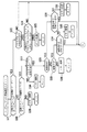
The information processing device according to
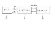
図1は、R/W1およびICカード2を利用した非接触カードシステムの一例を示している。R/W1およびICカード2は、電磁波を利用して非接触で、データの送受信を行う。
FIG. 1 shows an example of a contactless card system using an R /
R/W1が、所定のコマンドをICカード2に送信すると、ICカード2は、そのコマンドを受信し、そのコマンドに対応する処理を行うようになされている。
When the R /
本発明の情報処理装置の一実施の形態であるICカード2は、R/W1がデータをICカード2に送信すると、そのコマンドを受信し、受信したコマンドを処理し、その処理結果に対応する応答データをR/W1に送信するようになされている。
When the R /
また、R/W1は、所定のインタフェース(例えばRS−485A)を介してコントローラ3に接続され、コントローラ3より所定の制御信号を供給され、その制御信号に従って、処理を行うようになされている。
The R /
図2は、R/W1の構成を示している。 FIG. 2 shows the configuration of the R / W1.
IC21においては、データの処理を行うDPU(Data Processing Unit)31、ICカード2に送信するデータおよびICカード2から受信したデータの処理を行うSPU(Signal Processing Unit)32、コントローラ3との通信を行うSCC(Serial Communication Controller)33、および、データの処理に必要な情報を予め記憶しているROM部41と、処理途中のデータを一時的に記憶するRAM部42で構成されるメモリ部34が、バスを介して接続されている。
The
また、このバスには、所定のデータを記憶するフラッシュメモリ22も接続されている。
Further, a
DPU31は、ICカード2に送信するコマンドをSPU32に出力するとともに、ICカード2から受信した応答データをSPU32から受け取るようになされている。
The
SPU32は、ICカード2に送信するコマンドに対して所定の処理(例えば、BPSK(BiPhase Shift Keying)変調(後述))を行った後、変調回路23に出力するとともに、ICカード2により送信されてきた応答データを復調回路25から受け取り、そのデータに対して所定の処理を行うようになされている。
The
変調回路23は、発振器26より供給された所定の周波数(例えば13.56MHz)の搬送波を、SPU32より供給されたデータで、ASK(Amplitude Shift Keying)変調し、生成された変調波をアンテナ27を介して、電磁波としてICカード2に出力するようになされている。このとき、変調回路23は、変調度を1未満にして、ASK変調を行う。即ち、データがローレベルのときにおいても、変調波の最大振幅がゼロにならないようにする。
The
復調回路25は、アンテナ27を介して受信した変調波(ASK変調波)を復調し、復調されたデータをSPU32に出力するようになされている。
The
図3は、ICカード2の構成例を示している。このICカード2においては、IC51は、アンテナ53を介して、R/W1により送信された変調波を受信するようになされている。なお、コンデンサ52は、アンテナ53とともにLC回路を構成し、所定の周波数(キャリア周波数)の電磁波に同調するようになされている。
FIG. 3 shows a configuration example of the
IC51においては、RFインタフェース部61は、ASK復調部81で、アンテナ53を介して受信した変調波(ASK変調波)を検波して復調し、復調後のデータをBPSK復調回路62およびPLL(Phase Locked Loop)部63に出力するとともに、電圧レギュレータ82で、ASK復調部81が検波した信号を安定化し、各回路に直流電力として供給するようになされている。
In the
また、RFインタフェース部61は、発振回路83でデータのクロック周波数と同一の周波数の信号を発振し、その信号をPLL部63に出力するようになされている。
Further, the RF interface unit 61 oscillates a signal having the same frequency as the data clock frequency by the
そして、RFインタフェース部61のASK変調部84は、演算部64より供給されたデータに対応して、ICカード2の電源としてのアンテナ53の負荷を変動させる(例えば、データに対応して所定のスイッチング素子をオン/オフさせ、スイッチング素子がオン状態であるときだけ所定の負荷をアンテナ53に並列に接続させる)ことにより、アンテナ53を介して受信している変調波(ICカード2からデータを送信するときは、変調波の最大振幅を一定にしている)をASK変調し、その変調成分を、アンテナ53を介してR/W1に送信する(R/W1のアンテナ27の端子電圧を変動させる)ようになされている。
Then, the
PLL部63は、ASK復調部81より供給されたデータより、そのデータに同期したクロック信号を生成し、そのクロック信号をBPSK復調回路62およびBPSK変調回路68に出力するようになされている。
The
BPSK復調回路62は、ASK復調部81で復調されたデータが、BPSK変調されている場合、PLL部63より供給されたクロック信号に従って、そのデータの復調を行い、復調したデータを演算部64に出力するようになされている。
When the data demodulated by the
演算部64は、BPSK復調回路62より供給されたデータが暗号化されている場合、そのデータを暗号/復号部92で復号化した後、そのデータを、コマンドとして、シーケンサ91で処理するようになされている。なお、データが暗号化されていない場合、BPSK復調回路62より供給されたデータは、暗号/復号部92を介さず、シーケンサ91に、直接供給される。
When the data supplied from the
シーケンサ91は、供給されたコマンドに対応する処理を行うようになされている。例えば、このとき、シーケンサ91は、EEPROM66に記憶されているデータの処理を行う。
The
演算部64のパリティ演算部93は、EEPROM66に記憶されるデータや、EEPROM66に記憶されているデータから、パリティとして、リードソロモン符号を算出するようになされている。
The
さらに、演算部64は、シーケンサ91で所定の処理を行った後、その処理に対応する応答データ(R/W1に送信するデータ)をBPSK変調回路68に出力するようになされている。
Further, the
BPSK変調回路68は、演算部64より供給されたデータをBPSK変調し(後述)、変調後のデータをRFインタフェース部61のASK変調部84に出力するようになされている。
The
RAM67は、シーケンサ91が処理を行うとき、処理の途中のデータなどを、一時的に記憶するようになされている。
When the
EEPROM(Electrically Erasable and Programmable ROM)66は、不揮発性のメモリであり、ICカード2がR/W1との通信を終了し、電力供給が停止した後も、データを記憶し続けるようになされている。ROM65には、シーケンサ91がR/W1からのコマンドを処理するのに必要な基礎的なプログラムが記憶されている。
An EEPROM (Electrically Erasable and Programmable ROM) 66 is a non-volatile memory, and keeps storing data even after the
図4は、EEPROM66のメモリの割り当ての一例を示している。
FIG. 4 shows an example of memory allocation of the
EEPROM66は、40バイトの物理ブロックを、256個有している。各物理ブロックは、32バイトのデータ部(D00乃至D1f)、2バイトのアトリビュート部(AT1,AT2)、および、6バイトのパリティ部(P0乃至P5)の合計40バイトで構成されている。
The
EEPROM66の物理ブロック番号ffH(Hは16進数を表している)は、システムIDブロックに割り当てられている。システムIDブロックは、ICカード2のセキュリティに関する情報を記憶している。
The physical block number ffH (H represents a hexadecimal number) of the
次に、物理ブロック番号fdHから00Hに向かって順次、物理ブロックが、共通領域定義ブロック(Common Area Definition Block)(第1の領域)またはプロバイダ領域定義ブロック(Provider Area Definition Block)(第1の領域)に割り当てられている。 Next, in order from the physical block number fdH to 00H, the physical blocks are sequentially assigned to a common area definition block (Common Area Definition Block) (first area) or a provider area definition block (Provider Area Definition Block) (first area). ).
EEPROM66には、ICカード2が発行されるとき、所定の装置(発行機)により、このICカード2を利用したシステムを提供する者(プロバイダ)が登録される。発行機は、1プロバイダ当たり1物理ブロックで、プロバイダ領域定義ブロックを、物理ブロック番号fdHから00Hに向かって順次使用し、プロバイダを登録する。
When the
共通領域定義ブロックおよびプロバイダ領域定義ブロックは、プロバイダが使用する記憶領域の位置などの情報を記憶している。 The common area definition block and the provider area definition block store information such as the position of a storage area used by the provider.
そして、システムIDブロック、共通領域定義ブロック、およびプロバイダ領域定義ブロックとして利用されない物理ブロックが、プロバイダにより使用されるユーザブロック(User Block)に割り当てられる。 Then, physical blocks that are not used as the system ID block, the common area definition block, and the provider area definition block are allocated to user blocks (User Blocks) used by the provider.
図5は、システムIDブロックに対する各データの割り当ての一例を示している。 FIG. 5 shows an example of assignment of each data to the system ID block.
データ部のD00乃至D0fは、EEPROM66の製造時の製造ID(Manufacture ID)(IDm)が記憶されている。領域D00乃至D03、領域D04乃至D07、領域D08乃至D0b、および、領域D0c乃至D0fは、EEPROM66のICコード、EEPROM66を作成した製造機のコード(Manufacture Equipment Code)、EEPROM66の製造日(Manufacture Date)、および、EEPROM66の製造シリアルナンバ(Manufacture Serial Number)を、それぞれ記憶している。
D00 to D0f of the data section store a manufacturing ID (Manufacture ID) (IDm) at the time of manufacturing the
このIDmの情報を利用することにより、すべてのICカード2(EEPROM66)の識別を行うことができる。なお、製造日は、2000年1月1日を0000Hとして、2000年1月1日からの日数とする。なお、製造日が1990年台である場合、製造日は、2の補数を利用して、2000年1月1日からの負の日数として表現される。 By using the information of this IDm, all the IC cards 2 (EEPROM 66) can be identified. The date of manufacture is the number of days from January 1, 2000, with January 1, 2000 being 0000H. If the date of manufacture is in the 1990s, the date of manufacture is expressed as a negative number of days from January 1, 2000 using two's complement.
データ部のD10乃至D1fは、このIDカード2を発行したときの発行ID(Issue ID)(IDi)が記憶されている。領域D10乃至D13、領域D14乃至D17、領域D18乃至D1b、および、領域D1c乃至1fは、ICカード2の属するカテゴリおよびグループを示すカテゴリ/グループナンバ、このICカード2を発行した発行機のコード、ICカード2を発行した日にち、および、ICカード2の有効期限を、それぞれ記憶している。
D10 to D1f of the data section store an issue ID (Issue ID) (IDi) when the
図6は、システムIDブロックのアトリビュート部を示している。アトリビュート部は、登録されているプロバイダの数を記憶している。発行機は、1つのプロバイダを登録する際に、1つの物理ブロックを使用し、そのとき、このアトリビュート部の値を更新する。 FIG. 6 shows an attribute part of the system ID block. The attribute section stores the number of registered providers. When registering one provider, the issuing machine uses one physical block, and then updates the value of this attribute part.
アトリビュート部の値は、製造時に、ゼロに設定されており、その後、発行機が、ICカード2にプロバイダを登録するとき、アトリビュート部の値を、登録されるプロバイダの数で更新する。
The value of the attribute part is set to zero at the time of manufacture, and thereafter, when the issuing machine registers the provider in the
システムIDブロックのパリティ部は、データ部およびアトリビュート部の各ビットの値から、パリティ演算部93で演算されるリードソロモン符号(RS符号)を記憶している。従って、パリティ部の値は、データ部またはアトリビュート部が更新される度に、演算し直される。
The parity part of the system ID block stores a Reed-Solomon code (RS code) calculated by the
図7は、共通領域定義ブロックおよびプロバイダ領域定義ブロックの一例を示している。なお、これらのブロックは、ICカード2が発行されるとき、予め、発行機により書き込まれている。
FIG. 7 shows an example of the common area definition block and the provider area definition block. These blocks are written in advance by the issuing machine when the
共通領域定義ブロックは、EEPROM66の物理ブロック番号feHに配置され、全プロバイダにより使用される記憶領域(共通領域(Common Area))(第2の領域)の設定を記憶している。
The common area definition block is located at the physical block number feH of the
プロバイダ領域定義ブロックは、EEPROM66の物理ブロック番号fdHから、00Hに向かって配置され、1プロバイダ当たり1物理ブロックで、プロバイダの情報を記憶している。
The provider area definition block is arranged from the physical block number fdH of the
図7に示すように、領域定義ブロック(共通領域定義ブロックおよびプロバイダ領域定義ブロック)のデータ部D00乃至D1fの領域D00,D01は、プロバイダの種類を示すプロバイダコード(Provider Code)を記憶している。共 通領域定義ブロックの場合、領域D00,D01の値は、0000Hとされ、プロバイダ領域定義ブロックの場合、領域D00,D01の値は、0001H乃至FFFFHのいずれかの値とされている。 As shown in FIG. 7, the areas D00 and D01 of the data portions D00 to D1f of the area definition block (common area definition block and provider area definition block) store provider codes (Provider Code) indicating the type of provider. . In the case of the common area definition block, the values of the areas D00 and D01 are 0000H, and in the case of the provider area definition block, the values of the areas D00 and D01 are any one of 0001H to FFFFH.
領域定義ブロックのデータ部の領域D02乃至D05は、このプロバイダが使用する記憶領域(プロバイダ領域(Provider Area))(第2の領域)の先頭の物理ブロックの番号BN0(領域D02,D03)と、終わりの物理ブロックの番号の次の物理ブロックの番号BN1(領域D04,D05)(BN1>BN0)で構成されるアロケーションテーブル(Allocation Table)を記憶している。プロバイダ領域は、図8に示すように、システムブロック(システムIDブロック、領域定義ブロック)を除く、EEPROM66の所定の位置(物理ブロック番号BN0乃至(BN1−1))に設定される。
The areas D02 to D05 of the data part of the area definition block are the first physical block number BN 0 (areas D02 and D03) of the storage area (provider area) (second area) used by the provider. , An allocation table composed of a physical block number BN 1 (areas D04, D05) (BN 1 > BN 0 ) next to the last physical block number. As shown in FIG. 8, the provider area is set at a predetermined position (physical block numbers BN 0 to (BN 1 -1)) of the
このように、BN0とBN1でプロバイダ領域を指定しているので、プロバイダ(利用者)により使用される領域の大きさではなく、プロバイダの数に比例した量の情報で、データを管理することができ、メモリの利用効率を高くすることができる。 As described above, since the provider area is designated by BN 0 and BN 1 , the data is managed not with the size of the area used by the provider (user) but with information in an amount proportional to the number of providers. And the memory utilization efficiency can be increased.
領域定義ブロックのデータ部の領域D06乃至D09は、プロバイダが使用する記憶領域のうち、ランダムアクセス領域(後述)のブロック数BRA(領域D06,D07)と、ランダムアクセス領域中のリード/ライトブロックのブロック数BRW(領域D08,D09)で構成されるパーティションテーブル(Partition Table)を記憶している。このとき、ランダムアクセス領域のブロック数BRAは、式
BRA=0
または、式
2×n≦BRA≦BN1−BN0
(nはライトバッファ(後述)の数)
を満足する値に設定され、リード/ライトブロックのブロック数BRWは、BRA=0である場合においては、BRW=0に設定され、BRA≠0である場合においては、式
n≦BRW≦BRA−n
を満足する値に設定される。
The areas D06 to D09 of the data portion of the area definition block include, among the storage areas used by the provider, the number of blocks B RA (areas D06 and D07) of the random access area (described later) and the read / write blocks in the random access area. (Partition Table) composed of the number of blocks B RW (areas D08 and D09). At this time, the number of blocks B RA in the random access area is given by the following equation: B RA = 0
Or, the
(N is the number of write buffers (described later))
Is satisfied, and the number of read / write blocks B RW is set to B RW = 0 when B RA = 0, and the equation n ≦ when B RA n0. B RW ≦ B RA −n
Is satisfied.
領域定義ブロックのデータ部の領域D0a,D0bは、ランダムアクセス領域のライトバッファの数nを記憶している。n個のライトバッファは、n個のデータを、ランダムアクセス領域の論理ブロック番号00H乃至(00+n(16進数表示))Hに、同時に記憶させるときに利用される。なお、ランダムアクセス領域のうち、その他の論理ブロック番号を有する物理ブロックにデータを記憶するときにおいては、ライトバッファは、1個だけ利用される。 The areas D0a and D0b in the data section of the area definition block store the number n of write buffers in the random access area. The n write buffers are used when simultaneously storing n data in the logical block numbers 00H to (00 + n (hexadecimal notation)) H of the random access area. When data is stored in a physical block having another logical block number in the random access area, only one write buffer is used.
以上のように、領域定義ブロックに従って、図8に示すように、物理ブロック番号BN0乃至(BN1−1)の領域(プロバイダ領域または共通領域)は、プロバイダコードで指定されるプロバイダに割り当てられ、さらに、その領域(プロバイダ領域または共通領域)のうちのBRA個の物理ブロックが、ランダムアクセス領域に割り当てられ、残りの物理ブロックがシーケンシャルアクセス領域(後述)に割り当てられている。 As described above, according to the area definition block, as shown in FIG. 8, the area (provider area or common area) of the physical block numbers BN 0 to (BN 1 -1) is allocated to the provider specified by the provider code. Further, of the area (provider area or common area), BRA physical blocks are allocated to a random access area, and the remaining physical blocks are allocated to a sequential access area (described later).
さらに、領域定義ブロックに従って、図8に示すように、ランダムアクセス領域は、BRW個のリード/ライトブロック、リードオンリーブロック、および、n個のライトバッファに、論理的に割り当てられている。なお、リード/ライトブロックおよびライトバッファ以外の物理ブロックが、リードオンリーブロックに割り当てられる。 Further, according to the area definition block, as shown in FIG. 8, the random access area, B RW number of read / write block, a read only block and the n-number of write buffers are assigned logically. Note that physical blocks other than the read / write block and the write buffer are assigned to the read-only block.
領域定義ブロックのデータ部の領域D0c,D0dは、このプロバイダが利用する記憶領域(ランダムアクセス領域)におけるパースブロック(Purse Block)(後述)に対するアクセス権の情報を有するパースブロックパーミッションを記憶している。 The areas D0c and D0d of the data section of the area definition block store parse block permissions having access right information for a parse block (Purse Block) (described later) in a storage area (random access area) used by the provider. .
図9は、パースブロックパーミッションの一例を示している。 FIG. 9 shows an example of a parse block permission.
パースブロックパーミッション(16ビット、b0乃至bf)は、パースブロックに対する読み出し、加算命令、および、減算命令の許可または不許可を示している。 The parse block permission (16 bits, b 0 to b f ) indicates permission or non-permission of a read, an addition instruction, and a subtraction instruction for the parse block.
共通領域定義ブロックのパースブロックパーミッションは、共通領域定義ブロックで設定される記憶領域(共通領域)においてパースブロックを使用するか否かを、領域(ビット)bbに記憶している。即ち、bb=0の場合、パースブロックを使用しない。bb=1の場合、パースブロックを使用する。そして、共通領 域定義ブロックのパースブロックパーミッションにおけるその他の領域(ビット)は、特に使用されない。なお、bb=1の場合、論理ブロック番号が00Hで あるリード/ライトブロックが、パースブロックとして使用される。 Purse block permission of the common area definition block, whether to use a purse block in storage area set in the common area definition block (common area), stored in the area (bit) b b. That is, when b b = 0, no parse block is used. If b b = 1, use a parse block. Other areas (bits) in the parse block permission of the common area definition block are not particularly used. When b b = 1, the read / write block whose logical block number is 00H is used as a parse block.
次に、プロバイダ領域定義ブロックのパースブロックパーミッションにおいては、このプロバイダ領域定義ブロックで設定された記憶領域でパースブロックを使用するか否かを領域b3に記憶している。即ち、b3=0の場合、パースブロックを使用しない。b3=1の場合、パースブロックを使用する。なお、b3=1の場合、論理ブロック番号が00Hであるリード/ライトブロックが、パースブロックとして使用される。 Then, in the purse block permission of the provider area definition block, and stores whether or not to use the purse block in the region b 3 in the storage area set in the provider area definition block. That is, when b 3 = 0, no parse block is used. If b 3 = 1, use a parse block. When b 3 = 1, the read / write block whose logical block number is 00H is used as a parse block.
そして、そのパースブロックに対する加算命令の可否を領域b2に記憶し、そのパースブロックに対する減算命令の可否を領域b1に記憶し、そのパースブロックに対する読み出しの可否を領域b0に記憶している(bi=1(i=0,1,2)の場合、その命令は許可され、bi=0の場合、その命令は許可されない)。また、共通領域定義ブロックで設定された記憶領域でパースブロックを使用するか否かを領域bbに記憶している。なお、bbには、共通領域定義ブロックのパースブロックパーミッションのbbと同じ値が記憶されている。 The stores whether add instruction for that purse block in the region b 2, stores whether the subtraction instruction to the purse block in the area b 1, stores whether reading for that purse block in the region b 0 (If b i = 1 (i = 0, 1, 2), the instruction is allowed; if b i = 0, the instruction is not allowed). Also whether to use the purse block set storage area in the common area definition block is stored in the area b b. Note that the b b, the same value as b b Perth block permission of the common area definition block is stored.
さらに、そのパースブロックに対する加算命令の可否を領域baに記憶し、そのパースブロックに対する減算命令の可否を領域b9に記憶し、そのパースブロックに対する読み出しの可否を領域b8に記憶している(bi=1(i=8,9,a)の場合、その命令は許可され、bi=0の場合、その命令は許可されない)。 Further stores whether the add instruction for that purse block in the region b a, stores whether the subtraction instruction to the purse block in the region b 9, stores whether reading for that purse block in the region b 8 (If b i = 1 (i = 8, 9, a), the instruction is allowed; if b i = 0, the instruction is not allowed).
図7の領域定義ブロックのデータ部の領域D0e,D0fは、プロバイダ(R/W1)の認証、並びに、暗号化および復号化に利用されるセキュリティキー(共通鍵とプロバイダ鍵)のバージョン番号を記憶し、領域D10乃至1fは、そのセキュリティキーを記憶している。 The areas D0e and D0f of the data portion of the area definition block in FIG. 7 store the version numbers of the security keys (common key and provider key) used for authentication of the provider (R / W1) and encryption and decryption. The areas D10 to 1f store the security keys.
なお、R/W1がポーリングを行ったときは、ICカード2は、この2つのキー(共通鍵とプロバイダ鍵)のバージョン番号を返送する。従って、R/W1とICカード2との間の認証においては、複数のバージョンのセキュリティキーを使い分けることができる。
When the R /
そして、領域定義ブロックのアトリビュート部AT1,AT2は、予備として設けられており、特に情報は記憶されていない。領域定義ブロックのパリティ部は、データ部およびアトリビュート部のすべてのビットの値より演算されるパリティ(RS符号)を記憶している。 The attribute sections AT1 and AT2 of the area definition block are provided as spares, and no particular information is stored. The parity part of the area definition block stores a parity (RS code) calculated from the values of all bits of the data part and the attribute part.
このように、発行機により設定される領域定義ブロックは、プロバイダコード、アロケーションテーブル、パーティションテーブル、パースブロックパーミッション、セキュリティキーバージョン、および、セキュリティキーを記憶している。 As described above, the area definition block set by the issuing machine stores the provider code, the allocation table, the partition table, the parse block permission, the security key version, and the security key.
図10は、ユーザブロックの一例を示している。図4を参照して上述したように、EEPROM66のメモリ空間のうち、システムIDブロック、共通領域定義ブロック、プロバイダ領域定義ブロック以外の物理ブロックが、ユーザブロックとして、プロバイダにより使用される。
FIG. 10 shows an example of a user block. As described above with reference to FIG. 4, in the memory space of the
例えば、図4に示すように、メモリ空間が256ブロックで構成されている場合において、8個のプロバイダが登録されると、システムIDブロック、共通領域定義ブロック、および、8個のプロバイダ領域定義ブロックの合計10(=1+1+8)個のシステムブロック以外の、246(=256−10)ブロックがユーザブロックとして使用される。また、40個のプロバイダを登録すると、システムブロックは合計42(=1+1+40)個となり、214(=256−42)個のユーザブロックが確保される。 For example, as shown in FIG. 4, when the memory space is configured with 256 blocks, when eight providers are registered, a system ID block, a common area definition block, and eight provider area definition blocks are registered. , 246 (= 256-10) blocks other than the total of 10 (= 1 + 1 + 8) system blocks are used as user blocks. When 40 providers are registered, a total of 42 (= 1 + 1 + 40) system blocks are provided, and 214 (= 256-42) user blocks are secured.
ユーザブロックは、領域定義ブロックのアロケーションテーブル(図7)に従って、各プロバイダに割り当てられる。なお、プロバイダは、アロケーションテーブルを参照して、予め割り当てられているユーザブロックを使用するので、アロケーションテーブルで割り当てられた領域(プロバイダ領域または共通領域)以外にアクセスすることはない。 User blocks are assigned to each provider according to the allocation table of the area definition block (FIG. 7). Since the provider refers to the allocation table and uses the user blocks allocated in advance, the provider does not access any area other than the area (provider area or common area) allocated in the allocation table.
アロケーションテーブルで割り当てられた領域(プロバイダ領域または共通領域)のユーザブロックは、上述のパーティションテーブル(図7)に従って、ランダムアクセス領域と、シーケンシャルアクセス領域に割り当てられている。 The user blocks in the area (provider area or common area) allocated in the allocation table are allocated to a random access area and a sequential access area according to the above-described partition table (FIG. 7).
さらに、ランダムアクセス領域のユーザブロックは、リード/ライトブロック、リードオンリーブロック、および、ライトバッファのいずれかとして利用され、これらのブロックの数は、上述のように、パーティションテーブルおよびライトバッファの数に従って設定されている。 Further, the user block in the random access area is used as one of a read / write block, a read-only block, and a write buffer, and the number of these blocks depends on the number of partition tables and the number of write buffers as described above. Is set.
このように割り当てられているユーザブロックのデータ部D00乃至D1fは、そのユーザブロックが割り当てられているプロバイダによる処理に応じて使用される。 The data portions D00 to D1f of the user block allocated in this way are used in accordance with the processing by the provider to which the user block is allocated.
ランダムアクセス領域のユーザブロックのアトリビュート部は、図11に示すように、インクリメンタルカウンタ(Incremental Counter)(ビットbf,be)および論理ブロック番号(ビットbd乃至b0)を記憶している。 Attributes of the user block of random access area, as shown in FIG. 11, and stores the incremental counter (Incremental Counter) (bit b f, b e) and logical block number (bits b d to b 0).
論理ブロック番号とインクリメンタルカウンタは、ランダムアクセス領域のユーザブロックにアクセスするときに利用される。 The logical block number and the incremental counter are used when accessing a user block in the random access area.
ランダムアクセス領域に記憶されているデータを読み出すときにおいては、論理ブロック番号で、読み出すデータ(物理ブロック)を検索し、その論理ブロック番号を有するデータのインクリメンタルカウンタを参照して最も新しいデータを読み出す。 When reading the data stored in the random access area, the data (physical block) to be read is searched by the logical block number, and the newest data is read by referring to the incremental counter of the data having the logical block number.
一方、ランダムアクセス領域にデータを記憶する場合、既にランダムアクセス領域に記憶されているデータの論理ブロック番号とインクリメンタルカウンタを参照し、不要となった物理ブロック(後述)を、ライトバッファとした後、そのライトバッファにデータを書き込む。 On the other hand, when storing data in the random access area, by referring to the logical block number and the incremental counter of the data already stored in the random access area, an unnecessary physical block (described later) is used as a write buffer, and Write data to the write buffer.
なお、上述の領域定義ブロックのパースブロックパーミッションが、パースブロックを使用するように設定されている場合、論理ブロック番号が00Hであるリード/ライトブロックは、パースブロックとして使用される。 If the parse block permission of the area definition block is set to use a parse block, the read / write block whose logical block number is 00H is used as a parse block.
パースブロックは、データの加算および減算を頻繁に行うとき、既に記憶している値を読み出したくないとき(情報が漏洩する可能性が増すので)、データに対するアクセス権を細かく設定するときなどに利用される。 The parse block is used when frequently adding and subtracting data, when not wanting to read a value already stored (because the possibility of information leakage increases), and when setting detailed access rights to data. Is done.
図12は、パースブロックの一例を示している。パースブロックのデータ部D00乃至D1fの領域D00乃至D07は、パースデータ部として利用される。パースブロックのデータ部D00乃至D1fの領域D08乃至D0fは、エグゼキューションID(Execution ID)を記憶している。なお、パースブロックのデータ部の領域D10乃至D1fは、ユーザデータ部として利用されるが、読み出し専用に設定される。 FIG. 12 shows an example of a parse block. The areas D00 to D07 of the data parts D00 to D1f of the parse block are used as parse data parts. The areas D08 to D0f of the data parts D00 to D1f of the parse block store an execution ID (Execution ID). Note that the areas D10 to D1f of the data section of the parse block are used as user data sections, but are set to read-only.
パースデータ部は、所定のデータを記憶している。エグゼキューションIDは、パースブロックに対する加算命令または減算命令が実行されるときに参照され、その加算命令または減算命令に含まれているエグゼキューションIDと比較される。 The parse data section stores predetermined data. The execution ID is referred to when an addition instruction or a subtraction instruction for a parse block is executed, and is compared with the execution ID included in the addition instruction or the subtraction instruction.
一方、シーケンシャルアクセス領域のユーザブロックのアトリビュート部は、図13に示すように、ラップラウンド番号(ビットbf乃至b0)を記憶している。シーケンシャルアクセス領域には、領域の先頭の物理ブロックから順番に(シーケンシャルに)データが記憶されていき、領域の最後の物理ブロックまでデータが記憶されると、再び、領域の先頭の物理ブロックから順番にデータが記憶されていく(上書きされていく)。ラップラウンド番号は、その順番を記憶している。 On the other hand, the attribute of the user block of the sequential access area, as shown in FIG. 13, stores a wraparound number (bits b f to b 0). In the sequential access area, data is sequentially stored (sequentially) from the first physical block of the area. When data is stored up to the last physical block of the area, the data is again stored in order from the first physical block of the area. Are stored (overwritten). The lap round number stores the order.
従って、ラップラウンド番号は、シーケンシャルアクセス領域のユーザブロックにアクセスするときに利用されるとともに、シーケンシャルアクセス領域にデータを記憶する場合、順次参照される。そして、それまでの最後尾のラップラウンド番号を有する物理ブロックの次の物理ブロックに、データが記憶される。このとき、データが記憶された物理ブロックのラップラウンド番号は、それまでの最後尾のラップラウンド番号に1を加算した数に設定される。 Therefore, the wrap round number is used when accessing a user block in the sequential access area, and is sequentially referred to when data is stored in the sequential access area. Then, the data is stored in the physical block next to the physical block having the last wrap round number up to that time. At this time, the wrap round number of the physical block in which the data is stored is set to the number obtained by adding 1 to the last wrap round number up to that time.
なお、例えば前回の書込のときに書込の途中で障害が発生して、最後尾のラップラウンド番号を有する物理ブロックにパリティエラー(物理的なメモリコラプション)が生じている場合、新たなデータは、その物理ブロックに記憶される。また、最後尾のラップラウンド番号を有する物理ブロックがシーケンシャルアクセス領域の終わりの物理ブロックの場合、新たなデータは、シーケンシャルアクセス領域の先頭の物理ブロックに記憶される。 For example, when a failure occurs in the middle of writing at the time of previous writing and a parity error (physical memory corruption) occurs in the physical block having the last wrap round number, new data is written. Is stored in the physical block. If the physical block having the last wrap round number is the physical block at the end of the sequential access area, new data is stored in the first physical block of the sequential access area.
以上のように、EEPROM66は、各プロバイダに適宜利用される。
As described above, the
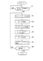
次に、図14のフローチャートおよび図15のタイミングチャートを参照して、ICカード2およびR/W1の動作について説明する。
Next, operations of the
最初にステップS1において、ICカード2に登録されているプロバイダに対応しているR/W1は、アンテナ27から所定の電磁波を放射して、アンテナ27の負荷状態を監視し、ICカード2が接近し、負荷状態の変化が検出されるまで待機する。なお、ステップS1においては、R/W1は、所定の短いパターンのデータでASK変調した電磁波を放射して、ICカード2への呼びかけを、ICカード2からの応答が一定時間内において得られるまで繰り返すようにしてもよい。
First, in step S1, the R /
R/W1がステップS1においてICカード2の接近を検出した場合(図15の時刻t0)、ステップS2に進み、R/W1のSPU32は、図16(a)に 示すような所定の周波数(例えば、データのクロック周波数の2倍の周波数)の矩形波を搬送波として、ICカード2に送信するデータ(ICカード2に実行させる処理に対応するコマンド)(例えば、図16(b)に示すデータ)で、BPSK変調を行い、生成した変調波(BPSK変調信号)(図16(c))を変調回路23に出力する。
When the R /
なお、BPSK変調時においては、差動変換を利用して、図16(c)に示すように、値が0のデータが現れた場合、直前のBPSK変調信号(「1」「0」または「0」「1」)と同じものをBPSK変調信号とし、値が1のデータが現れた場合、直前のBPSK変調信号の位相を反転させたもの(「1」を「0」に反転させ、「0」を「1」に反転させたもの)をBPSK変調信号としている。 At the time of BPSK modulation, when data having a value of 0 appears as shown in FIG. 16C using differential conversion, the immediately preceding BPSK modulation signal (“1” “0” or “ The same signal as “0” and “1” is used as a BPSK modulation signal, and when data having a value of 1 appears, a signal obtained by inverting the phase of the immediately preceding BPSK modulation signal (“1” is inverted to “0” and “ "0" is inverted to "1") as a BPSK modulation signal.
このように差動変換を利用して、変調波の位相の変化でデータを保持することにより、BPSK変調信号が反転した場合も、元のデータに復調されるので、復調するとき変調波の極性を配慮する必要が無くなる。 As described above, the data is held by the change in the phase of the modulated wave using the differential conversion, so that even if the BPSK modulation signal is inverted, the data is demodulated to the original data. There is no need to consider.
そして、変調回路23は、そのBPSK変調信号で、所定の搬送波を1未満(例えば0.1)の変調度(=データ信号の最大振幅/搬送波の最大振幅)でASK変調させ、生成された変調波(ASK変調波)を、アンテナ27を介してICカード2に送信する(図15の時刻t0乃至時刻t1の間)。
Then, the
なお、送信を行わないとき、変調回路23は、デジタル信号の2つのレベル(ハイレベルとローレベル)のうちのハイレベルで変調波を生成するようになされている。
When transmission is not performed, the
次にステップS3において、ICカード2は、アンテナ53およびコンデンサ52で、R/W1のアンテナ27が放射した電磁波の一部を電気信号に変換し、その電気信号(変調波)を、IC51のRFインタフェース部61に出力する。そして、RFインタフェース部61のASK復調部81は、その変調波を整流および平滑し(即ち、包絡線検波し)、生成された信号を電圧レギュレータ82に供給するとともに、生成された信号の直流成分を抑制してデータ信号を抽出し、そのデータ信号をBPSK復調回路62およびPLL部63に出力する。
Next, in step S3, the
電圧レギュレータ82は、ASK復調部81より供給された信号を安定化し、直流電力を生成し、各回路に供給する。
The
なお、このとき、アンテナ53の端子電圧V0は、例えば次のようになる。
V0=V10(1+k×Vs(t))cos(ωt)
At this time, the terminal voltage V 0 of the
V 0 = V 10 (1 + k × Vs (t)) cos (ωt)
ここで、V10は、搬送波成分の振幅を、kは変調度を、Vs(t)は信号成分を、それぞれ示している。 Here, V 10 is the amplitude of the carrier component, k is the modulation depth, Vs (t) is a signal component, respectively.
また、ASK復調部81による整流後の電圧V1におけるローレベルの値VLRは、例えば次のようになる。
VLR=V10(1+k×(−1))−Vf
The value V LR of low level in the voltage V 1 of the post-rectification by the
V LR = V 10 (1 + k × (−1)) − Vf
ここで、Vfは、整流回路のダイオードDにおける電圧降下を示している。通常Vfは0.7ボルト程度である。 Here, Vf indicates a voltage drop in the diode D of the rectifier circuit. Usually, Vf is about 0.7 volt.
そして、電圧レギュレータ82は、ASK復調部81により整流および平滑された信号を安定化し、直流電力として、演算部64を始めとする各回路に供給する。なお、変調波の変調度kは1未満であるので、整流後の電圧変動(ハイレベルとローレベルの差)が小さい。従って、電圧レギュレータ82は、直流電力を容易に生成することができる。
Then, the
例えば、変調度kが5%の変調波を、V10が3ボルト以上になるように受信した場合、整流後のローレベル電圧VLRは、2.15(=3×(1−0.05)−0.7)ボルト以上となり、電圧レギュレータ82は、電源として充分な電圧を各回路に供給することができるとともに、整流後の電圧V1の交流成分(データ 成分)の振幅2×k×V10(Peak-to-Peak値)は、0.3(=2×0.05×3)ボルト以上になり、ASK復調部81は、十分高いS/N比でデータの復調を行うことができる。
For example, when the modulation degree k is 5% of the modulation wave, received as V 10 is equal to or greater than 3 volts, the low level voltage V LR after the rectification, 2.15 (= 3 × (1-0.05 ) -0.7) becomes volts or more, the
このように、変調度kが1未満のASK変調波を利用することにより、エラーレートの低い(S/N比の高い状態で)通信を行うとともに、電源として充分な直流電圧がICカード2に供給される。
As described above, by using the ASK modulated wave having the modulation factor k of less than 1, communication with a low error rate (in a state of a high S / N ratio) is performed, and a sufficient DC voltage as a power supply is supplied to the
そして、BPSK復調回路62は、PLL部63より供給されるクロック信号に従って、ASK復調部81からのデータ信号(BPSK変調信号)を復調し、復調したデータを演算部64に出力する。
Then, the
次に、ステップS4において、演算部64は、BPSK復調回路62より供給されたデータが暗号化されている場合は、暗号/復号部92で復号化した後、そのデータ(コマンド)をシーケンサ91に供給し、そのコマンドに対応する処理を行う(図15の時刻t1乃至時刻t2の間)。なお、この期間、即ちICカード2からの返答を受信するまでの間、R/W1は、値が1のデータを送信したまま待機している。従って、この期間においては、ICカード2は、最大振幅が一定である変調波を受信している。
Next, in step S4, if the data supplied from the
次に、ステップS5において、演算部64のシーケンサ91は、処理結果などのデータ(R/W1に送信するデータ)を、BPSK変調回路68に出力する。BPSK変調回路68は、R/W1のSPU32と同様に、そのデータをBPSK変調した後、RFインタフェース部61のASK変調部84に出力する。
Next, in step S5, the
そして、ASK変調部84は、アンテナ53の両端に接続される負荷を、スイッチング素子を利用してデータに応じて変動させることにより、受信している変調波(ICカード2の送信時においては、変調波の最大振幅は一定になっている)を、送信するデータに応じてASK変調させ、それに応じてR/W1のアンテナ27の端子電圧を変動させて、そのデータをR/W1に送信する(図15の時刻t2乃至時刻t3の間)。
Then, the
ステップS6において、R/W1の変調回路23は、ICカード2からのデータの受信時においても、値が1(ハイレベル)のデータの送信を継続している。そして、復調回路25は、ICカード2のアンテナ27と電磁気的に結合しているアンテナ27の端子電圧の微小な変動(例えば、数十マイクロボルト)から、ICカード2により送信されてきたデータを検出する。
In step S6, the
そして、復調回路25は、検出した信号(ASK変調波)を高利得の増幅器で増幅した後、復調し、生成されたデジタルデータをSPU32に出力する。
Then, the
そして、ステップS7において、R/W1のSPU32は、そのデータ(BPSK変調信号)を復調した後、DPU31に出力し、DPU31は、そのデータを処理する(図15の時刻t3乃至時刻t4の間)。
Then, in step S7,
さらに、ステップS8において、R/W1のDPU31は、処理結果に応じて、通信を終了するか否かを判断し、再度、通信を行うと判断した場合、ステップS2に戻り、ステップS2乃至ステップS7で、次のデータ(コマンド)の通信を行う(図15の時刻t4乃至時刻t8)。一方、通信を終了すると判断した場合、R/W1は、ICカード2との通信を終了する。
Further, in step S8, the
以上のように、R/W1は、変調度kが1未満であるASK変調を利用して、ICカード2に所定のコマンドを送信し、ICカード2は、そのコマンドを受け取り、そのコマンドに対応する処理を行って、その処理の結果に対応するデータを、R/W1に返送する。
As described above, the R /
次に、上述のステップS4におけるICカード2による処理の例として、EEPROM66に対してデータの書込を行うときの動作について、図17乃至図21のフローチャートを参照して説明する。
Next, as an example of the processing by the
最初に、図17乃至図19のフローチャートを参照して、EEPROM66のランダムアクセス領域にデータを書き込むときの動作について説明する。
First, an operation when writing data in the random access area of the
ステップS21において、シーケンサ91は、データを書き込む物理ブロックがリード/ライトブロック(パースブロックは含まない)である(図8に示すように、BN0から順番に、BRW個までのブロックはリード/ライトブロックとされる)か否かを判断し、リード/ライトブロックであると判断した場合、ステップS22に進む。
In step S21, the
シーケンサ91は、R/W1のプロバイダコードを有するプロバイダ領域定義ブロックのパースブロックパーミッション(図9)を参照し、パースブロックを使用している(b3=1)か否かを判断し、パースブロックを使用していない場
合(b3=0の場合)、ステップS23(図18)に進む。
The
一方、ステップS22においてパースブロックを使用していると判断した場合、シーケンサ91は、ステップS24において、記憶する(書き込む)データの論理ブロック番号が00Hであるか否か、即ち、データを書き込むリード/ライトブロックがパースブロックと重なっているか否かを判断し、データを書き込むリード/ライトブロックがパースブロックと重なっていないと判断した場合、ステップS23に進む。
On the other hand, if it is determined in step S22 that a parse block is being used, the
データを書き込むリード/ライトブロックがパースブロックと重なっていると判断した場合、シーケンサ91は、ステップS25において、エラー処理を行った後、処理を終了する。
If it is determined that the read / write block to which data is to be written overlaps the parse block, the
また、ステップS21においてデータを書き込む物理ブロックがリード/ライトブロックではないと判断した場合、ステップS26に進み、シーケンサ91は、データを書き込む物理ブロックがパースブロックであるか否かを判断し、パースブロックであると判断した場合、ステップS27に進む。
If it is determined in step S21 that the physical block to which data is to be written is not a read / write block, the process proceeds to step S26, where the
データを書き込む物理ブロックがパースブロックではないと判断した場合、シーケンサ91は、ステップS28において、エラー処理を行った後、処理を終了する。
If it is determined that the physical block in which the data is to be written is not a parse block, the
ステップS27において、シーケンサ91は、ランダムアクセス領域において、パースブロック(論理ブロック番号が00Hの物理ブロック)を探し、パースブロックを発見した場合、ステップS29に進む。
In step S27, the
ステップS27でパースブロックが発見されなかった場合、パースブロックに対する書込を行うことができないので、シーケンサ91は、ステップS30において、エラー処理を行った後、処理を終了する。
If a parse block is not found in step S27, writing to the parse block cannot be performed, so the
次に、ステップS29において、シーケンサ91は、そのパースブロックに対する命令(コマンド)が加算命令であるか否かを判断し、加算命令であると判断した場合、ステップS31に進み、プロバイダ領域定義ブロックのパースブロックパーミッションを参照して、加算命令が許可されているか(b2=1)否かを判断する。
Next, in step S29, the
そして、ステップS31で、シーケンサ91が、パースブロックに対する加算命令が許可されていると判断した場合、ステップS23に進む。
Then, in step S31, when the
一方、ステップS31で、パースブロックに対する加算命令が許可されていないと判断した場合(b2=0の場合)、シーケンサ91は、加算命令を実行せずに、ステップS32において、エラー処理を行った後、処理を終了する。
On the other hand, if it is determined in step S31 that the addition instruction for the parse block is not permitted (in the case of b 2 = 0), the
また、ステップS29において、パースブロックに対する命令が加算命令ではないと判断した場合、ステップS33に進み、シーケンサ91は、そのパースブロックに対する命令が減算命令であるか否かを判断し、減算命令であると判断した場合、ステップS34に進む。
If it is determined in step S29 that the instruction for the parse block is not an addition instruction, the process proceeds to step S33, where the
そして、ステップS34において、シーケンサ91は、プロバイダ領域定義ブロックのパースブロックパーミッションを参照して、減算命令が許可されている(b1=1)か否かを判断し、パースブロックに対する減算命令が許可されていると判断した場合、ステップS23に進む。
Then, in step S34, the
一方、ステップS34で、パースブロックに対する減算命令が許可されていないと判断した場合(b1=0の場合)、シーケンサ91は、減算命令を実行せずに、ステップS35において、エラー処理を行った後、処理を終了する。
On the other hand, when it is determined in step S34 that the subtraction instruction for the parse block is not permitted (when b 1 = 0), the
また、ステップS33において、パースブロックに対する命令が減算命令ではないと判断した場合、シーケンサ91は、ステップS36において、エラー処理を行った後、処理を終了する。
If it is determined in step S33 that the instruction for the parse block is not a subtraction instruction, the
次に、図18のステップS23において、シーケンサ91は、ランダムアクセス領域の物理ブロックを検索して、書込を行うデータの論理ブロック番号と同一の論理ブロック番号を有する物理ブロックを探す。
Next, in step S23 in FIG. 18, the
そして、ステップS37において、シーケンサ91は、ステップS23で発見した物理ブロックの数が2個であるか否かを判断する。すなわち、このシステムにおいては、各論理ブロックについて、少なくとも、前回のデータと、前々回のデータを記憶するようにする。そして、さらに新たなデータを記憶するときは、前々回のデータの上に新たなデータを記憶する(他の論理ブロック番号の前々回のデータの上に記憶される場合もある)。同一の論理ブロック番号の物理ブロックが2個存在する場合、ステップS38に進み、その2つの物理ブロックにおけるインクリメンタルカウンタの値(00,01,10,11のいずれか)を読み出し、比較する。
Then, in step S37, the
そして、インクリメンタルカウンタの値が大きい物理ブロックを、新しいデータが記憶されている物理ブロック(新しい物理ブロック)とし、インクリメンタルカウンタの値が小さい物理ブロックを、古いデータが記憶されている物理ブロック(古い物理ブロック)とする。 Then, a physical block having a large incremental counter value is defined as a physical block storing new data (new physical block), and a physical block storing a small incremental counter value is defined as a physical block storing old data (old physical block). Block).
ただし、2つのインクリメンタルカウンタの値が00と11である場合は、インクリメンタルカウンタの値が00である物理ブロックを、新しい物理ブロックとし、インクリメンタルカウンタの値が11である物理ブロックを、古い物理ブロックとする。 However, when the values of the two incremental counters are 00 and 11, the physical block whose incremental counter value is 00 is set as a new physical block, and the physical block whose incremental counter value is 11 is replaced with an old physical block. I do.
ステップS39において、シーケンサ91は、2つの物理ブロックのうち、新しい物理ブロックの番号(物理ブロック番号)を、変数Yとして、RAM67に記憶し、古い物理ブロックの番号を、変数W(ライトブロックとして利用される物理ブロックの番号)として、RAM67に記憶させる。
In step S39, the
このように、シーケンサ91が、変数Yと変数Wを記憶させた後、ステップS49に進む。
After the
一方、ステップS37において、ステップS23で発見した物理ブロックの数が2個ではないと判断した場合、ステップS40に進み、シーケンサ91は、ステップS23で発見した物理ブロックの数が1個であるか否かを判断する。そして、1個であると判断した場合、ステップS41に進む。
On the other hand, if it is determined in step S37 that the number of physical blocks found in step S23 is not two, the process proceeds to step S40, and the
ステップS40において、シーケンサ91が、ステップS23で発見した物理ブロックの数が1個ではないと判断した場合、ステップS42において、エラー処理を行った後、処理を終了する。
If the
同一の論理ブロックが1個しか存在しないということは、何等かの理由により、前々回のデータが存在しないことになる。そこで、この場合は、他の論理ブロック番号の物理ブロックで、前回と前々回のデータを有する物理ブロック(すなわち、同一の論理ブロック番号を有する物理ブロックの数が2個である物理ブロック)を検索し、そのうちの前々回の物理ブロックをライトブロックとして利用する。このため、ステップS41において、シーケンサ91は、発見した物理ブロック(1個)の番号を、変数Yとして、RAM67に記憶させた後、ステップS43に進む。
The fact that there is only one identical logical block means that, for some reason, the data before the previous one does not exist. Therefore, in this case, a physical block having another logical block number is searched for a physical block having data of the previous and previous times (ie, a physical block having two physical blocks having the same logical block number). The physical block of the last two times is used as a write block. For this reason, in step S41, the
ステップS43において、シーケンサ91は、ランダムアクセス領域の物理ブロックを検索して、所定の(任意の)同一の論理ブロック番号(いま書込対象としている論理ブロック番号とは無関係の論理ブロック番号)を有する2個の物理ブロックを探す。
In step S43, the
なお、物理ブロックを検索するときは、論理ブロック番号00Hから順次検索していくので、頻繁に書込処理を行うデータの論理ブロック番号を、より小さい番号すると、検索時間を短くすることができる。 When searching for a physical block, the search is performed sequentially from the logical block number 00H. Therefore, if the logical block number of the data to be frequently written is smaller, the search time can be shortened.
そして、ステップS44において、シーケンサ91は、論理ブロック番号が同一である2個の物理ブロックがステップS43で発見されたか否かを判断し、発見されたと判断した場合、ステップS45に進み、発見された2個の物理ブロックのインクリメンタルカウンタを参照し、2個の物理ブロックのうち、古い方の物理ブロックの番号を、変数W(ライトブロックの番号)として、RAM67に記憶させた後、ステップS49(図19)に進む。
Then, in step S44, the
一方、ステップS44において、ステップS43で2個の物理ブロックが発見されなかったと判断した場合、ステップS46に進み、シーケンサ91は、ランダムアクセス領域の各物理ブロックのパリティを順次計算して、各物理ブロックのパリティ部に記憶されている値と比較し、パリティエラーを起こしている物理ブロックを探す。
On the other hand, if it is determined in step S44 that two physical blocks have not been found in step S43, the process proceeds to step S46, where the
そして、パリティエラーを起こしている物理ブロックがあるか否かを判断し、パリティエラーを起こしている物理ブロックがあると判断した場合、ステップS47に進み、シーケンサ91は、その物理ブロックの番号を、変数W(ライトブロックの番号)として、RAM67に記憶させた後、ステップS49に進む。
Then, it is determined whether or not there is a physical block having a parity error. If it is determined that there is a physical block having a parity error, the process proceeds to step S47, and the
ステップS46において、パリティエラーを起こしている物理ブロックがないと判断した場合、シーケンサ91は、ステップS48において、エラー処理を行った後、処理を終了する。
If it is determined in step S46 that there is no physical block having a parity error, the
次に、図19のステップS49において、シーケンサ91は、データを書き込む物理ブロックがパースブロック(論理ブロック番号が00Hである物理ブロック)であるか否かを判断し、パースブロックであると判断した場合、ステップS50に進み、パースブロックに対して行われる命令のエグゼキューションIDが、ステップS39またはステップS41で変数Yとして記憶された番号の物理ブロックのエグゼキューションID(図12)と同一であるか否かを判断し、同一であると判断した場合、この命令は既に処理されていると判断し、処理を終了する。
Next, in step S49 in FIG. 19, the
このようにエグゼキューションIDを利用することにより、R/W1が同じコマンドをリトライした場合において、そのコマンドが既に処理されているときは、ICカード2は、そのコマンドの処理を行わないので、同じコマンドが2度処理されることはない。
By using the execution ID in this way, if the R /
ステップS50において、パースブロックに対して行われる命令のエグゼキューションIDが、変数Yとして記憶された番号の物理ブロックのエグゼキューションIDと同一ではないと判断した場合、シーケンサ91は、ステップS51において、パースブロックに対して行われる命令が加算命令であるか否かを判断し、加算命令である場合、ステップS52に進む。
If it is determined in step S50 that the execution ID of the instruction executed for the parse block is not the same as the execution ID of the physical block having the number stored as the variable Y, the
ステップS52において、シーケンサ91は、変数Yの番号の物理ブロックのパースデータを読み出し、そのパースデータと、パースブロックに対して行われる命令に含まれているデータの和を計算し、その和を新規ブロックデータにおけるパースデータ(新規パースデータ)とする。このように処理を行った後、ステップS54に進む。なお、このとき、変数Yの番号の物理ブロックのエグゼキューションIDを新規ブロックデータのエグゼキューションIDとする。これにより2重の処理を防止する。
In step S52, the
一方、ステップS51において、パースブロックに対して行われる命令が加算命令ではない(即ち、減算命令である)と判断した場合、ステップS53に進み、シーケンサ91は、変数Yの番号の物理ブロックのパースデータを読み出し、そのパースデータと、パースブロックに対して行われる命令に含まれているデータの差を計算し、その差を新規ブロックデータにおけるパースデータ(新規パースデータ)とする。このように処理を行った後、ステップS54に進む。なお、このとき、変数Yの番号の物理ブロックのエグゼキューションIDを新規ブロックデータのエグゼキューションIDとする。これにより2重の処理を防止する。
On the other hand, if it is determined in step S51 that the instruction performed on the parse block is not an addition instruction (that is, a subtraction instruction), the process proceeds to step S53, where the
また、ステップS49において、シーケンサ91は、データを書き込む物理ブロックがパースブロックではない(即ち、リード/ライトブロックである)と判断した場合、ステップS54に進む。
If the
そして、ステップS54において、シーケンサ91は、変数Yの番号の物理ブロックのインクリメンタルカウンタの値に1を加算した数を、新規ブロックデータのインクリメンタルカウンタの値とする。ただし、変数Yの番号の物理ブロックのインクリメンタルカウンタの値が11である場合、シーケンサ91は、新規ブロックデータのインクリメンタルカウンタの値を00とする。
Then, in step S54, the
次に、ステップS55において、シーケンサ91は、パリティ演算部93に、新たに書き込むデータ、インクリメンタルカウンタおよび論理ブロック番号のパリティを計算させ、そのパリティの値を、新規ブロックデータのパリティ部の値とする。
Next, in step S55, the
そして、ステップS56において、シーケンサ91は、ステップS39、ステップS45、または、ステップS47のいずれかで記憶された変数Wの番号の物理ブロック(ライトバッファ)に、新規ブロックデータ(新たに記憶するデータ(パースブロックの場合、パースデータとエグゼキューションID)、その論理ブロック番号、インクリメンタルカウンタ、および、これらのパリティ)を記憶させる。
Then, in step S56, the
以上のように、論理ブロック番号と、インクリメンタルカウンタを利用して、データを記憶する物理ブロック(ライトバッファ)を選択することにより、データの書込の最中に、障害が発生した場合においても、そのデータの論理ブロック番号と同一の論理ブロック番号のデータがメモリに残されているので、論理的には、メモリコラプションが発生することはない。 As described above, by selecting a physical block (write buffer) for storing data using the logical block number and the incremental counter, even if a failure occurs during data writing, Since data having the same logical block number as the logical block number of the data is left in the memory, logically, memory corruption does not occur.
上記実施の形態では、ランダムアクセス領域の同一の論理ブロックのうち、新しいデータが記録されているブロックを判別するためにインクリメンタルカウンタを用いたが、例えば、記録時の絶対時刻(日付と時刻、あるいはカウンタの値)をランダムアクセス領域に、例えば4バイトの領域を確保して、そこに記録させることによって、新しいデータが記録されているブロックを判別することも可能である。 In the above embodiment, among the same logical blocks in the random access area, the incremental counter is used to determine a block in which new data is recorded. For example, an absolute time (date and time, or For example, by securing an area of, for example, 4 bytes in the random access area and recording it in the random access area, it is possible to determine a block in which new data is recorded.
次に、図20および図21のフローチャートを参照して、EEPROM66のシーケンシャルアクセス領域にデータを書き込むときの動作について説明する。
Next, an operation of writing data in the sequential access area of the
ステップS61において、シーケンサ91は、シーケンシャルアクセス領域の先頭の物理ブロックの番号を、変数Zとして、RAM67に記憶させる。
In step S61, the
次に、ステップS62において、シーケンサ91は、物理ブロック番号がZである物理ブロックのラップラウンド番号を読み出し、変数Aとして、RAM67に記憶させるとともに、物理ブロック番号がZ+1である物理ブロックのラップラウンド番号を読み出し、変数Bとして、RAM67に記憶させる。
Next, in step S62, the
そして、ステップS63において、シーケンサ91は、変数Aの値と変数Bの値の差(A−B)が1であるか否かを判断し、1ではない場合、物理ブロック番号Zの物理ブロックが、最後尾のラップラウンド番号を有するデータを記憶する物理ブロックであると判断し、ステップS66に進む。
Then, in step S63, the
変数Aの値と変数Bの値の差(A−B)が1であると判断した場合、シーケンサ91は、ステップS64において、物理ブロック番号Zが、シーケンシャルアクセス領域の終わりの物理ブロックの番号と同一であるか否かを判断し、同一であると判断した場合、シーケンシャルアクセス領域の終わりの物理ブロックが、最後尾のラップラウンド番号を有するデータを記憶する物理ブロックであると判断し、ステップS66に進む。
When determining that the difference (A−B) between the value of the variable A and the value of the variable B is 1, the
ステップS64において、物理ブロック番号Zが、シーケンシャルアクセス領域の終わりの物理ブロックの番号と同一ではないと判断した場合、シーケンサ91は、ステップS65において、RAM67に記憶させた変数Zの値を1だけ増加させた後、ステップS62に戻る。そして、ステップS62乃至ステップS65の処理を、変数Zの値(検索する物理ブロック番号の値)を変化させながら順次繰り返す。
If it is determined in step S64 that the physical block number Z is not the same as the number of the physical block at the end of the sequential access area, the
このようにして、シーケンシャルに記憶されているデータのラップラウンド番号の最後尾を発見する。そして、ステップS66において、シーケンサ91は、変数Zの番号(=ラップラウンド番号の最後尾の物理ブロックの番号)のブロックのパリティチェックを行う。
In this way, the end of the wrap round number of the data stored sequentially is found. Then, in step S66, the
そして、ステップS67において、シーケンサ91は、その物理ブロックにパリティエラーが生じているか否かを判断し、パリティエラーが生じていると判断した場合、ステップS68に進む。
Then, in step S67, the
ステップS68において、シーケンサ91は、変数Zの値が、シーケンシャルアクセス領域の先頭の物理ブロックの番号と同一であるか否かを判断し、同一であると判断した場合、データ(パリティエラーを起こしているものは含まない)の最後尾が、シーケンシャルアクセス領域の終わりの物理ブロックであると判断し、ステップS70において、シーケンシャルアクセス領域の終わりの物理ブロックの番号を、新たな変数Yとして、RAM67に記憶させた後、ステップS72(図21)に進む。
In step S68, the
変数Zの値が、シーケンシャルアクセス領域の先頭の物理ブロックの番号と同一ではないと判断した場合、ステップS71において、シーケンサ91は、データの最後尾の物理ブロックの番号を、変数Zの値から1を減算して算出し、算出した値(Z−1)を、変数Yとして、RAM67に記憶させた後、ステップS72に進む。
When determining that the value of the variable Z is not the same as the number of the first physical block in the sequential access area, the
一方、ステップS67でパリティエラーが生じていないと判断した場合、ステップS69において、シーケンサ91は、データの最後尾の物理ブロックの番号(この場合、変数Zの値)を、変数Yとして、RAM67に記憶させた後、ステップS72に進む。
On the other hand, if it is determined in step S67 that a parity error has not occurred, in step S69, the
次に、ステップS72において、シーケンサ91は、データの最後尾の物理ブロックの番号(変数Yの値)と、シーケンシャルアクセス領域の終わりの物理ブロックの番号が同一であるか否かを判断し、同一であると判断した場合、ステップS73に進む。
Next, in step S72, the
そして、ステップS73において、シーケンサ91は、シーケンシャルアクセス領域の先頭の物理ブロックの番号を、新たなデータを書き込む物理ブロックの番号とし、その番号を変数Wとして、RAM67に記憶させた後、ステップS75に進む。
Then, in step S73, the
ステップS72においてデータの最後尾の物理ブロックの番号(変数Yの値)と、シーケンシャルアクセス領域の終わりの物理ブロックの番号が同一ではないと判断した場合、ステップS74において、シーケンサ91は、変数Yの値に1を加算した数を、新たなデータを書き込む物理ブロックの番号とし、その番号を変数Wとして、RAM67に記憶させた後、ステップS75に進む。
If it is determined in step S72 that the number of the last physical block of the data (the value of the variable Y) and the number of the physical block at the end of the sequential access area are not the same, the
次にステップS75において、シーケンサ91は、新たに記憶するデータと、変数Yの番号の物理ブロック(最後尾のデータ)が同一であるか否かを判断し、同一である場合、新たに記憶するデータが既に記憶されているので、処理を終了する。
Next, in step S75, the
一方、新たに記憶するデータと、変数Yの番号の物理ブロック(最後尾のデータ)が同一ではないと判断された場合、ステップS76において、シーケンサ91は、変数Yの番号の物理ブロックのラップラウンド番号を読み出し、その値に1を加算した数を、新たに記憶されるデータ(新規ブロックデータ)のラップラウンド番号とする。
On the other hand, if it is determined that the data to be newly stored is not the same as the physical block (the last data) of the number of the variable Y, in step S76, the
次にステップS77において、シーケンサ91は、パリティ演算部93に、記憶するデータおよびラップラウンド番号(新規ブロックデータ)のパリティを演算させ、ステップS78において、番号Wの物理ブロックに新規ブロックデータを書き込む。
Next, in step S77, the
このように、シーケンシャルに記憶されているデータにおけるラップラウンド番号を順次検索していき、最後尾のデータの次の物理ブロック(または、シーケンシャルアクセス領域の先頭の物理ブロック)に、新たなデータを記憶するので、新たなデータの書込の最中に、障害が発生した場合においても、書き込んでいたデータのラップラウンド番号より小さいラップラウンド番号のデータが残っているので、論理的には、メモリコラプションは発生しない。 As described above, the wrap round number in the data stored sequentially is sequentially searched, and new data is stored in the next physical block of the last data (or the first physical block of the sequential access area). Therefore, even if a failure occurs during the writing of new data, data of a wrap round number smaller than the wrap round number of the written data remains, so logically, memory corruption Does not occur.
以上のように、EEPROM66は、複数のプロバイダに対して、独立に記憶領域を提供することができるとともに、アトリビュート部の情報を利用して、メモリコラプションの発生を抑制するようになされている。
As described above, the
なお、複数のプロバイダに対して、同一のユーザブロックを割り当てることもできる。その場合、それらのプロバイダ(オーバラッププロバイダ)が登録されているプロバイダ領域定義ブロックのアロケーションテーブルで、同一のユーザブロックを割り当てるようにする。このとき、各プロバイダ毎に、プロバイダ領域定義ブロックのパーティションテーブルを設定することにより、同一のユーザブロックに対して、プロバイダ毎に異なるアクセス権(リード/ライトまたはリードオンリー)を設定することができる。さらに、所定のプロバイダに対してはパースブロックを使用しないように設定し、他のプロバイダに対してはパースブロックを使用するように設定することにより、所定のプロバイダは、他のプロバイダが使用するパースブロックのユーザデータ部(他のプロバイダに対しては読み出し専用)に対して、データの書込を行うことができる。 Note that the same user block can be assigned to a plurality of providers. In this case, the same user block is allocated in the allocation table of the provider area definition block in which those providers (overlap providers) are registered. At this time, by setting the partition table of the provider area definition block for each provider, different access rights (read / write or read only) can be set for the same user block for each provider. Further, by setting the parse block not to be used for a given provider and by setting the parse block to be used for another provider, the given provider is able to use the parse block used by the other provider. Data can be written to the user data portion of the block (read only for other providers).
また、領域定義ブロックの領域D0e,D0f(通常、セキュリティキーのバージョン番号が記憶されている領域)の値を、所定の値(例えば、FFFFH)に設定し、さらに、領域定義ブロックの領域D10乃至D1fに、所定のプロバイダのプロバイダコード(最大8個)を記憶することにより、そのプロバイダ(ローカルコモンプロバイダ)は、この領域定義ブロックのアロケーションテーブルで割り当てられるユーザブロックを、共通領域として使用することができる。 Also, the values of the areas D0e and D0f (usually areas where the security key version number is stored) of the area definition block are set to predetermined values (for example, FFFFH). By storing the provider code (up to eight) of a predetermined provider in D1f, the provider (local common provider) can use a user block allocated in the allocation table of the area definition block as a common area. it can.
また、同一のユーザブロックを割り当てる2つの領域定義ブロックに、ローカルコモンプロバイダを登録し、領域定義ブロック毎に、異なるアクセス権を設定することにより、そのユーザブロックに対するアクセス権を、ローカルコモンプロバイダ毎に設定することができる。 In addition, the local common provider is registered in two area definition blocks to which the same user block is assigned, and different access rights are set for each area definition block, so that the access right to the user block is set for each local common provider. Can be set.
このように、オーバラッププロバイダおよびローカルコモンプロバイダを設定することにより、複数のプロバイダ(即ち、R/W)に対応して個別の処理を行うことができる。 In this way, by setting the overlap provider and the local common provider, it is possible to perform individual processing corresponding to a plurality of providers (ie, R / W).
なお、本発明は、電波(非接触)で信号を授受する場合の他、物理的に結合された状態(接触)で信号を授受する場合にも適用することができる。停電の場合、あるいは、電池で動作する装置において、電池が取り外されてしまったような場合に、データを確保しておくことができる。 Note that the present invention can be applied to a case where signals are transmitted and received in a physically coupled state (contact), in addition to a case where signals are transmitted and received by radio waves (non-contact). In the case of a power outage, or in a case where a battery has been removed from a battery-operated device, data can be secured.
また、上記各処理を行うプログラムは、磁気ディスク、CD−ROMなどの記録媒体よりなる伝送媒体に記録してユーザに提供したり、ネットワークなどの伝送媒体を介してユーザに伝送し、ハードディスク、固体メモリなどの記録媒体よりなる伝送媒体に記録し、利用させるようにすることができる。 Further, the program for performing each of the above-described processes is recorded on a transmission medium such as a magnetic disk or a CD-ROM and provided to the user, or transmitted to the user via a transmission medium such as a network. It can be recorded on a transmission medium such as a recording medium such as a memory and used.
1 リーダ/ライタ, 2 ICカード, 3 コントローラ, 21 IC, 23 変調回路, 25 復調回路, 27 アンテナ, 51 IC, 52 コンデンサ, 53 アンテナ, 61 RFインタフェース部, 62 BPSK復調回路, 63 PLL部, 64 演算部, 65 ROM, 66 EEPROM, 67 RAM, 68 BPSK変調回路, 81 ASK復調部, 82 電圧レギュレータ, 83 発振回路, 84 ASK変調部, 91 シーケンサ, 92 暗号/復号部, 93 パリティ演算部 1 reader / writer, 2 IC card, 3 controller, 21 IC, 23 modulation circuit, 25 demodulation circuit, 27 antenna, 51 IC, 52 capacitor, 53 antenna, 61 RF interface section, 62 BPSK demodulation circuit, 63 PLL section, 64 Operation unit, 65 ROM, 66 EEPROM, 67 RAM, 68 BPSK modulation circuit, 81 ASK demodulation unit, 82 voltage regulator, 83 oscillation circuit, 84 ASK modulation unit, 91 sequencer, 92 encryption / decryption unit, 93 parity operation unit
Claims (5)
前記コマンドを処理する処理手段と、
前記処理の結果を送信する送信手段と、
前記プロバイダの装置が利用するデータを記憶するとともに、1以上のユーザブロックが所定の大きさのブロック単位で管理されるユーザブロック領域と、前記ユーザブロックの利用を定義する領域定義ブロック領域が形成される記憶手段と
を備え、
前記領域定義ブロック領域は、複数の領域定義ブロックからなり、
前記領域定義ブロックは、1つの前記ユーザブロックに対して複数の前記領域定義ブロックを割り当てるように定義される
ことを特徴とする情報処理装置。 Receiving means for receiving a command from a device of a provider providing a predetermined system;
Processing means for processing the command;
Transmitting means for transmitting a result of the processing,
In addition to storing data used by the provider device, a user block area in which one or more user blocks are managed in block units of a predetermined size, and an area definition block area defining use of the user block are formed. Storage means and
The area definition block area includes a plurality of area definition blocks,
The information processing apparatus according to claim 1, wherein the area definition block is defined such that a plurality of the area definition blocks are assigned to one user block.
ことを特徴とする請求項1に記載の情報処理装置。 2. The information processing apparatus according to claim 1, wherein the plurality of area definition blocks assigned to one user block are two or more area definition blocks having different data defining access rights. 3. .
ことを特徴とする請求項2に記載の情報処理装置。 The information processing apparatus according to claim 2, wherein the data defining the access right is data defining one of read / write access and read-only access to the user block in the user block area. .
前記プロバイダの装置からのコマンドを受信する受信ステップと、
前記領域定義ブロック領域を基に、前記コマンドを処理する処理ステップと、
前記処理の結果を送信する送信ステップと
を含むことを特徴とする情報処理方法。 A user block area for storing data used by a device of a provider that provides a predetermined system and in which one or more user blocks are managed in block units of a predetermined size, and an area definition for defining use of the user blocks An information processing apparatus including a storage unit in which a block area is formed, wherein the area definition block area includes a plurality of area definition blocks, and a plurality of the area definition blocks are assigned to one user block. In the information processing method of the information processing device defined,
A receiving step of receiving a command from the provider device;
A processing step of processing the command based on the area definition block area;
A transmitting step of transmitting a result of the processing.
前記プロバイダの装置からのコマンドの受信を制御する受信制御ステップと、
前記領域定義ブロック領域を基に、前記コマンドを処理する処理ステップと、
前記処理の結果の送信を制御する送信制御ステップと
を含むことを特徴とするコンピュータが読み取り可能なプログラムが記録されている記録媒体。 A user block area for storing data used by a device of a provider that provides a predetermined system and in which one or more user blocks are managed in block units of a predetermined size, and an area definition for defining use of the user blocks An information processing apparatus including a storage unit in which a block area is formed, wherein the area definition block area includes a plurality of area definition blocks, and a plurality of the area definition blocks are assigned to one user block. In the defined information processing program of the information processing apparatus,
A reception control step of controlling reception of a command from the provider device;
A processing step of processing the command based on the area definition block area;
A transmission control step of controlling transmission of a result of the processing, wherein a computer-readable program is recorded.
Priority Applications (1)
| Application Number | Priority Date | Filing Date | Title |
|---|---|---|---|
| JP2004188866A JP3890602B2 (en) | 1996-06-28 | 2004-06-25 | Information processing apparatus, information processing method, and recording medium |
Applications Claiming Priority (2)
| Application Number | Priority Date | Filing Date | Title |
|---|---|---|---|
| JP16896696 | 1996-06-28 | ||
| JP2004188866A JP3890602B2 (en) | 1996-06-28 | 2004-06-25 | Information processing apparatus, information processing method, and recording medium |
Related Parent Applications (1)
| Application Number | Title | Priority Date | Filing Date |
|---|---|---|---|
| JP17143097A Division JP4462646B2 (en) | 1996-06-28 | 1997-06-27 | Information processing apparatus, information processing method, reader / writer, access method, and recording medium |
Publications (2)
| Publication Number | Publication Date |
|---|---|
| JP2004342123A true JP2004342123A (en) | 2004-12-02 |
| JP3890602B2 JP3890602B2 (en) | 2007-03-07 |
Family
ID=33542793
Family Applications (1)
| Application Number | Title | Priority Date | Filing Date |
|---|---|---|---|
| JP2004188866A Expired - Lifetime JP3890602B2 (en) | 1996-06-28 | 2004-06-25 | Information processing apparatus, information processing method, and recording medium |
Country Status (1)
| Country | Link |
|---|---|
| JP (1) | JP3890602B2 (en) |
Families Citing this family (2)
| Publication number | Priority date | Publication date | Assignee | Title |
|---|---|---|---|---|
| JP4631935B2 (en) | 2008-06-06 | 2011-02-16 | ソニー株式会社 | Information processing apparatus, information processing method, program, and communication system |
| JP5272637B2 (en) | 2008-10-14 | 2013-08-28 | ソニー株式会社 | Information processing apparatus, encryption switching method, and program |
-
2004
- 2004-06-25 JP JP2004188866A patent/JP3890602B2/en not_active Expired - Lifetime
Also Published As
| Publication number | Publication date |
|---|---|
| JP3890602B2 (en) | 2007-03-07 |
Similar Documents
| Publication | Publication Date | Title |
|---|---|---|
| US7752406B2 (en) | Information processing method and information processing apparatus having data locations accessible by different devices in accordance with different permissions | |
| JP3721725B2 (en) | Information processing method and information processing apparatus | |
| JP4051510B2 (en) | Data storage device and data storage method | |
| US8756384B2 (en) | Information processing device and information processing method for data recovery after failure | |
| JP2004054394A (en) | Radio information processing system, radio information recording medium, radio information processor and communication method for radio information processing system | |
| JP3702923B2 (en) | Information processing method and information processing apparatus | |
| US7376973B2 (en) | Data storage apparatus | |
| JP4462646B2 (en) | Information processing apparatus, information processing method, reader / writer, access method, and recording medium | |
| JP3890602B2 (en) | Information processing apparatus, information processing method, and recording medium | |
| JP3890603B2 (en) | Information processing apparatus, information processing method, reader / writer, access method, and recording medium | |
| JPH1139450A (en) | Ic card | |
| JP2003030609A (en) | Portable information processor | |
| JP2007086934A (en) | Rfid tag | |
| JP2005309975A (en) | Data communication system, method, and device |
Legal Events
| Date | Code | Title | Description |
|---|---|---|---|
| A977 | Report on retrieval |
Free format text: JAPANESE INTERMEDIATE CODE: A971007 Effective date: 20060517 |
|
| A131 | Notification of reasons for refusal |
Free format text: JAPANESE INTERMEDIATE CODE: A131 Effective date: 20060619 |
|
| A521 | Request for written amendment filed |
Free format text: JAPANESE INTERMEDIATE CODE: A523 Effective date: 20060818 |
|
| TRDD | Decision of grant or rejection written | ||
| A01 | Written decision to grant a patent or to grant a registration (utility model) |
Free format text: JAPANESE INTERMEDIATE CODE: A01 Effective date: 20061113 |
|
| A61 | First payment of annual fees (during grant procedure) |
Free format text: JAPANESE INTERMEDIATE CODE: A61 Effective date: 20061126 |
|
| FPAY | Renewal fee payment (event date is renewal date of database) |
Free format text: PAYMENT UNTIL: 20171215 Year of fee payment: 11 |
|
| EXPY | Cancellation because of completion of term |