JP2004340950A - Navigation device using interference - Google Patents
Navigation device using interference Download PDFInfo
- Publication number
- JP2004340950A JP2004340950A JP2004119296A JP2004119296A JP2004340950A JP 2004340950 A JP2004340950 A JP 2004340950A JP 2004119296 A JP2004119296 A JP 2004119296A JP 2004119296 A JP2004119296 A JP 2004119296A JP 2004340950 A JP2004340950 A JP 2004340950A
- Authority
- JP
- Japan
- Prior art keywords
- optical
- navigation device
- optical radiation
- phase pattern
- mouse
- Prior art date
- Legal status (The legal status is an assumption and is not a legal conclusion. Google has not performed a legal analysis and makes no representation as to the accuracy of the status listed.)
- Withdrawn
Links
Images


Classifications
-
- G—PHYSICS
- G06—COMPUTING; CALCULATING OR COUNTING
- G06F—ELECTRIC DIGITAL DATA PROCESSING
- G06F3/00—Input arrangements for transferring data to be processed into a form capable of being handled by the computer; Output arrangements for transferring data from processing unit to output unit, e.g. interface arrangements
- G06F3/01—Input arrangements or combined input and output arrangements for interaction between user and computer
- G06F3/03—Arrangements for converting the position or the displacement of a member into a coded form
- G06F3/0304—Detection arrangements using opto-electronic means
- G06F3/0317—Detection arrangements using opto-electronic means in co-operation with a patterned surface, e.g. absolute position or relative movement detection for an optical mouse or pen positioned with respect to a coded surface
-
- G—PHYSICS
- G06—COMPUTING; CALCULATING OR COUNTING
- G06F—ELECTRIC DIGITAL DATA PROCESSING
- G06F3/00—Input arrangements for transferring data to be processed into a form capable of being handled by the computer; Output arrangements for transferring data from processing unit to output unit, e.g. interface arrangements
- G06F3/01—Input arrangements or combined input and output arrangements for interaction between user and computer
- G06F3/03—Arrangements for converting the position or the displacement of a member into a coded form
- G06F3/033—Pointing devices displaced or positioned by the user, e.g. mice, trackballs, pens or joysticks; Accessories therefor
- G06F3/0354—Pointing devices displaced or positioned by the user, e.g. mice, trackballs, pens or joysticks; Accessories therefor with detection of 2D relative movements between the device, or an operating part thereof, and a plane or surface, e.g. 2D mice, trackballs, pens or pucks
- G06F3/03543—Mice or pucks
Abstract
Description
本発明は、運動検知装置に関し、更に詳しくは、光学位相パターン画像を使用して相対運動を判定するシステム及び方法に関するものである。 The present invention relates to motion detection devices, and more particularly, to systems and methods for determining relative motion using an optical phase pattern image.
既存の光学相対運動検出装置においては、装置が表面上を通過する際に(或いは、これと等価的に表面が装置を通過する際に)表面の画像を取得することにより、画像相関法を利用して装置と表面間の相対運動を判定している。1つの画像を次のものと比較することにより、装置による運動の距離と方向の両方が判定される。この技法は、通常、表面上における影の強度変動を検出するものであり、その感度と有用性は、取得した表面画像における強度のコントラストによって左右される。相対運動センサは、例えば、コンピュータのポインタ(例:マウス)の制御に使用されており、このようなポインタは、通常、オプティクスを使用してコンピュータ画面上のポインタの位置を制御している。 Existing optical relative motion detectors utilize image correlation techniques by acquiring an image of the surface as it passes over the surface (or equivalently, as the surface passes over the device). To determine the relative motion between the device and the surface. By comparing one image to the next, both the distance and direction of motion by the device are determined. This technique typically detects intensity variations of shadows on the surface, the sensitivity and usefulness of which depends on the intensity contrast in the acquired surface image. Relative motion sensors are used, for example, to control computer pointers (eg, a mouse), and such pointers typically use optics to control the position of the pointer on a computer screen.
特許文献1、特許文献2、特許文献3、特許文献4、特許文献5、及び特許文献6の各明細書には、光学マウス、その他の携帯型ナビゲーション装置、及び携帯型スキャナの例が記述されている。これらの特許の内容は、この引用により、本明細書に包含される。
The specifications of
通常の既存の装置の場合には、例えば、ガラスやホワイトボードなどの鏡のような(又は、光沢のある)表面、均一な表面、又は浅い形状を有する表面においては、十分に機能しない。このような装置は、画像のコントラストを改善するべく、通常、正反射を遮断し、表面からの散乱光学放射のみを取得しており、この方法によれば、電力及び光学放射の使用効率が大幅に制限されることになる。又、使用する表面は、通常、影を投影する能力を有していなければならない。一般に、これは、観測対象の表面における形状が、使用する光学放射の波長に対応した光学形状範囲内の寸法を備えていなければならないことを意味している。従って、この電力の非効率的な使用法と表面タイプにおける制約が現在の光学マウス設計における代表的な欠点となっている。 Typical existing devices do not work well on mirror-like (or glossy) surfaces, such as glass or whiteboard, uniform surfaces, or surfaces with shallow shapes. Such devices typically block specular reflections and obtain only scattered optical radiation from the surface to improve image contrast, which significantly increases the efficiency of power and optical radiation use. Will be limited to Also, the surface used must typically have the ability to cast shadows. Generally, this means that the shape at the surface to be observed must have dimensions within the optical shape range corresponding to the wavelength of the optical radiation used. Therefore, this inefficient use of power and limitations on surface types are typical drawbacks in current optical mouse designs.
本発明によれば、物体に対する移動を判定する光学ナビゲーション装置が提供される。この装置は、物体を照射する光学放射源と、光学放射が物体から戻ってきた後に、光学放射における位相パターンを取得する検出器と、を含んでおり、これらの位相パターンは、物体の光学的な不均一性と相関している。尚、本明細書において使用するこの「光学放射」という用語は、約1ナノメートル(nm)〜約1ミリメートル(mm)の波長範囲における電磁放射を含んでいる。又、本明細書において使用する「光学的な不均一性」という用語は、光学放射ビームと相互作用する能力を有し、相互作用する光学放射ビーム内の位相パターンを変化させる(例えば、粒状、形状、反射率、スペクトル、又は散在による不均質性や不規則性などの)意図的及び非意図的な表面又は容積の不規則性を含んでいる。 According to the present invention, there is provided an optical navigation device for determining movement with respect to an object. The apparatus includes an optical radiation source that illuminates the object, and a detector that obtains a phase pattern in the optical radiation after the optical radiation returns from the object, wherein the phase patterns are based on optical characteristics of the object. Is correlated with significant non-uniformity. It should be noted that the term "optical radiation" as used herein includes electromagnetic radiation in the wavelength range from about 1 nanometer (nm) to about 1 millimeter (mm). Also, as used herein, the term "optical inhomogeneity" refers to the ability to interact with an optical radiation beam and change the phase pattern within the interacting optical radiation beam (e.g., granular, Includes intentional and unintentional surface or volume irregularities (such as shape, reflectivity, spectral, or scattered inhomogeneities and irregularities).
本発明によれば、光学ナビゲーション装置と物体間の相対的な移動を判定する方法は、物体を照射する光学放射ビームを提供する段階と、この光学放射が物体から戻ってきた後に、光学放射における位相パターンを判定する段階と、を含んでいる。 According to the present invention, a method for determining relative movement between an optical navigation device and an object includes providing a beam of optical radiation illuminating the object and, after the optical radiation returns from the object, the optical radiation. Determining a phase pattern.
本発明によれば、センサと物体間の相対的な移動の表示を制御する方法は、センサが物体に対して移動した際に一連のインターフェログラムを生成する段階と、生成されたインターフェログラムの連続したペア間における相関の関数として相対的な移動の視覚表現を表示する段階と、を含んでいる。 According to the present invention, a method for controlling an indication of relative movement between a sensor and an object includes the steps of generating a series of interferograms when the sensor moves relative to the object; Displaying a visual representation of the relative movement as a function of the correlation between successive pairs of.
本発明によれば、物体に対する移動を検出するマウスを使用してコンピュータの画面上の位置ポインタを制御するシステムが提供される。このシステムは、その上をマウスが移動する物体の一部に対してそれぞれが固有のものになっている複数のインターフェログラムを生成する手段と、この固有のインターフェログラムの連続したペアをマウスと物体間の相対的な移動に対応する信号に変換する手段と、を含んでいる。 In accordance with the present invention, there is provided a system for controlling a position pointer on a computer screen using a mouse that detects movement relative to an object. The system consists of a means for generating multiple interferograms, each unique to a part of the object over which the mouse moves, and a continuous pair of these unique interferograms. And means for converting the signal into a signal corresponding to the relative movement between the objects.
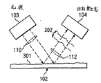
図1は、本発明による光学ナビゲーションシステム100を示す概略ブロックダイアグラムであり、図2は、本発明による光学ナビゲーションシステム100を使用する方法において必要とされる操作を示すフローチャートである。光学ナビゲーションシステム100は、光学装置101と、この光学装置101に対して(矢印107、108によって示されているように)2次元の面内においてあらゆる方向に運動可能な物体102と、の間における相対位置を判定するものである。
FIG. 1 is a schematic block diagram illustrating an
まず、操作201において、物体102は、光学装置101の光源103からの光学放射ビーム110によって照射される。次いで、操作202において、この光学放射ビーム110は、物体102との相互作用によって処理され、この結果、この光学放射ビーム110内の位相パターンは、物体102から伝播してくる(例:物体を透過又は物体から反射してくる)出射光学放射ビーム112において変化する。従って、本発明による実施例の中には、出射光学放射ビーム112内の位相パターンを、例えば、物体102の表面106における反射又は散乱による光学放射ビーム110の相互作用によって変化させるものが存在している。更には、この代わりに、例えば、物体102を貫通して光学放射ビーム110が透過する際に発生する相互作用により、位相パターンを変化させることも可能である。次いで、操作203において、この位相パターンが変化した出射光学放射ビーム112を位相検出器104によって検出する。
First, in operation 201, an
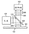
図3A〜図3Cは、本発明による光学ナビゲーションに関連する位相パターンの変化の基本原理を示す図である。まず、図3Aにおいては、照射された光源103からの光学放射ビーム110が、物体102の表面301において反射している。尚、図示を容易にするべく、平行化されたものとして光学放射ビーム110を示し、且つ表面301を不規則なでこぼこの表面として示しているが、本発明においては、このような平行化や不規則なでこぼこの表面は、いずれも必要とされるものではない。表面301から出射する反射光学放射ビーム112は、表面301と光学放射ビーム110の相互作用の結果生成された位相パターン302を含んでいる。この位相パターン302は、光学放射ビーム110によって照射された表面301の特定部分の固有の特性を表すものである。この反射光学放射ビーム112を位相検出器104によって取得し、処理して信号を生成する(この信号からは、後程、位相パターン302内に含まれている情報を抽出することができる)。又、位相検出器104は、後程詳述するように、この取得の前に、位相パターンが変化した光学放射ビーム112を更に処理するべく構成することができる。
3A to 3C are diagrams illustrating the basic principle of phase pattern change related to optical navigation according to the present invention. First, in FIG. 3A, an emitted
図3Bは、通常、その内部が光学的に不均一な物体307を通じた透過による光源103からの光学放射ビーム110の位相パターンの変化を示している。図3Aと同様に、位相パターン309を有する透過光学放射ビーム308を位相検出器104によって取得し、必要に応じて、更なる処理を施す。この位相パターン309は、光学放射ビーム110が通過した物体307の特定容積部分の固有の特徴を表している。一方、図3Cにおいては、図3Aと同様に、光源103からの光学放射ビーム110が反射すると共に、その位相パターンが物体102の表面301によって変化している。しかしながら、この場合には、光学放射ビーム110は、まず、ビームスプリッタ303に水平に入射しており、このビームの一部304をビームスプリッタが下向きに表面301上に部分反射している。そして、位相パターン306を有する反射光学放射ビーム305がビームスプリッタ303を通じて上方に部分透過した後に、画像検出器322によって取得され、必要に応じて、更なる処理が施される。
FIG. 3B shows a change in the phase pattern of the
ここで、再度、図1及び図2を参照すれば、操作204において、位相検出器104は、位相パターンが変化した出射光学放射ビーム112の画像を取得し、画像信号114が生成される。この検出は、例えば、CCD、CMOS、GaAs、アモルファスシリコン、又はその他の適切な検出器アレイなどのアレイ画像化装置によって実行可能である。通常、光源103から放射される光学放射ビーム110の波長スペクトルを、このアレイ画像化装置の波長応答に適合させる。次いで、画像信号114を画像プロセッサ105に伝送し、ここで、操作205において、画像に更なる処理が施され、操作206において、画像信号114に応答し出力信号116が生成される。画像プロセッサ105においては、例えば、画像の連続したペアを比較する相関アルゴリズムを使用する従来の方法により、相対移動を判定するための画像処理を実行することができる。本発明による実施例の中には、タイミング信号を利用して相対速度を判定できるものも存在する。出力信号116は、例えば、コンピュータ画面上のポインタの位置を駆動するべく構成可能である。
Referring again to FIGS. 1 and 2, in
光源103と位相検出器104は、通常、光学的な完全性を考慮して光学装置101内に一緒に内蔵されている。又、任意選択により、画像プロセッサ105を光学装置101内に内蔵することも可能である(但し、画像プロセッサは、光学ナビゲーションシステム100内のどこか別の場所に配置することもできる)。本発明による実施例の中には、光学装置101がコンピュータシステム用の光学マウスになっており、任意選択により、ユーザーが手で操作可能なものも存在している。
The
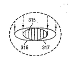
図3D〜図3Eは、本発明による位相検出器に適用する平行板干渉計を示す図である。後面312に平行な前面311を備える平行板310上に光学放射ビーム110が導波される。そして、前面311において、光学放射ビーム110は、光線313b、314bによって示されているように部分反射する共に、光線313a、314aによって示されているように部分屈折する。次いで、屈折した光線313a、314aは、後面312によって、個々の反射光線313c、314cに部分反射され、次いで、これらが、前面311において、個々の透過光線313d、314dに屈折し、光線313b、314bによって定義される反射光学放射ビームとオーバーラップすると共にオフセットされた光学放射ビームを定義している。図3Eの詳細図に示されているように、オフセットされたビームのそれぞれは、領域316、317を照射しており、これら両方のオフセットビームは、いずれもオーバーラップ領域315を照射している。これらのオフセットビームは、いずれも単一の光学放射ビーム110によるものであるため、オーバーラップ領域315内には干渉パターンが生成されることになる。この干渉パターンは、2つのオーバーラップしたビームのずれの方向における位相関数の傾きに対応している。
3D to 3E are views showing a parallel plate interferometer applied to the phase detector according to the present invention. The
本発明によれば、通常、画像を取得する前に、位相パターンが変化した光学放射ビーム112を処理するべく、位相検出器104に干渉計を内蔵している。本明細書に記述されている概念の基礎をなす光学インターフェロメトリは、従来、表面解析と計測に広く使用されているものである(例えば、非特許文献2の1〜7章を参照されたい。尚、この内容は、この引用により、本明細書に包含される)。インターフェロメトリの利点には、通常、波長以下のスケールの感度と精度が含まれている。
In accordance with the present invention, an interferometer is typically included in
図3Dの平行板構造は、通常のシアリング干渉計の一種と見なすことが可能であり、光学干渉は、位相パターンが変化した光学フィールドと、この位相パターンが変化した光学フィールドの変位バーションと、が空間的にオーバーラップする結果生成される。観測される干渉縞は、直接的には、オリジナルの光学フィールドの位相関数の傾きを、そして、結果的には、表面形状の傾き関数に関連付けることができる。シアリング干渉計は、表面解析に広く使用されており、シアリング干渉計は、その共通経路構成のために、その他のタイプの干渉計と比べ、丈夫であって、振動や温度変化の影響を受けにくい。又、この共通経路構成により、低コヒーレンス光源を使用することができる。尚、本明細書において使用するこの「低コヒーレンス」という用語は、時間的な低コヒーレンス(即ち、広がったスペクトル幅又はいずれか一時点と前の(又は、後の)時点における光源からの光学放射の振幅及び/又は位相間の強い相関の欠如)と、空間的な低コヒーレンス(即ち、光源からの光学放射ビームの2つの点における波面の瞬間的な振幅間及び瞬間的な位相角度間における強い相関の欠如)の両方を含んでいる(例えば、非特許文献3参照)。低コヒーレンス光源には、例えば、発光ダイオード(LED)などのダイオードエミッタ、マルチモード垂直共振器面発光レーザー(VCSEL)、及びその他のマルチモードレーザーダイオードタイプや白色灯が含まれる(例えば、非特許文献1参照。尚、この内容は、この引用により、本明細書に包含される)。例えば、低しきい値のVCSEL光源(通常、約2mAの電流を使用するもの)を使用すれば、従来使用されているLED(通常、約30mAの電流を使用するもの)に比べ、電力消費量を削減することができる。再度図3Cを参照し、この図に示されている構造がシアリング干渉計の一種と見なすことができることを認識されたい。 The parallel plate structure of FIG. 3D can be considered as a type of ordinary shearing interferometer, where the optical interference is based on the optical field with the changed phase pattern, the displacement version of the optical field with the changed phase pattern, Are spatially overlapped. The observed fringes can be directly related to the slope of the phase function of the original optical field and, consequently, to the slope function of the surface shape. Shearing interferometers are widely used for surface analysis, and due to their common path configuration, shearing interferometers are more robust and less susceptible to vibration and temperature changes than other types of interferometers . Also, with this common path configuration, a low coherence light source can be used. As used herein, the term "low coherence" refers to low coherence in time (i.e., broadened spectral width or optical emission from a light source at any one time and before (or after) a point in time). Lack of strong correlation between the amplitude and / or phase of the light) and the spatially low coherence (ie, between the instantaneous amplitude and instantaneous phase angle of the wavefront at two points of the optical radiation beam from the light source). (Lack of correlation)) (for example, see Non-Patent Document 3). Low coherence light sources include, for example, diode emitters such as light emitting diodes (LEDs), multi-mode vertical cavity surface emitting lasers (VCSELs), and other multi-mode laser diode types and white lamps (see, eg, Non-Patent Documents). 1, the contents of which are hereby incorporated by reference). For example, using a low-threshold VCSEL light source (which typically uses about 2 mA of current) would consume less power than a conventionally used LED (typically using about 30 mA of current). Can be reduced. Referring again to FIG. 3C, it should be appreciated that the structure shown in this figure can be considered a type of shearing interferometer.
シアリング干渉計は、通常、その他のタイプの干渉計を上回る利点を提供するが、本発明による光学ナビゲーション技法は、シアリング干渉計に限定されるものではなく、所望の特定のアプリケーションに応じて異なるタイプの干渉計を利用することができる。本発明において使用可能なタイプの代替干渉計には、例えば、Michelson(Twyman−Green)、Mach−Zehnder、Fizeau、及び単一又は複数の回折要素を備える干渉計の実装が含まれる。これらの干渉計の更に詳細な説明については、例えば、引用によって既に本明細書に包含されている非特許文献2の1〜7章を参照されたい。
Although shearing interferometers typically offer advantages over other types of interferometers, the optical navigation techniques according to the present invention are not limited to shearing interferometers, but different types depending on the particular application desired. Can be used. Alternative interferometers of the type that can be used in the present invention include, for example, Michelson (Tyman-Green), Mach-Zehnder, Fizeau, and interferometer implementations with single or multiple diffractive elements. For a more detailed description of these interferometers, see, for example,
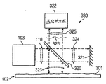
図3F〜図3Gは、Michelson(Twyman−Green)及びMach−Zehnder干渉計を含む本発明において使用可能な一般的な代替干渉計のタイプを示す図である。図3Fは、Twyman−Green干渉計の原理を示す図である。これは、図3Cに示されている構造に類似しており、光学放射ビーム110は、反射光学放射ビーム323として、ビームスプリッタ320から部分反射され、物体102の不規則な表面301を照射する。しかしながら、透過光学放射ビーム324として、ビームスプリッタ320を透過した光学放射ビーム110の部分は、ミラー321によって反射してビームスプリッタ320上に戻り、次いで、上方に部分反射される。この上方に部分反射した光学放射ビーム324は、次いで、表面301における反射後の位相パターン326を有する光学放射ビーム325とオーバーラップする。このオーバーラップしたビーム324及び325を画像検出器322によって取得するのである。
3F-3G illustrate common alternative interferometer types that can be used in the present invention, including Michelson (Tyman-Green) and Mach-Zehnder interferometers. FIG. 3F is a diagram illustrating the principle of the Twyman-Green interferometer. This is similar to the structure shown in FIG. 3C, where the
図3Gの場合には、ビームスプリッタ341において、Mach−Zehnder干渉計は、基準ビーム346として、光源103からの光学放射ビーム110を部分反射すると共に、透過ビーム344として、光学放射ビーム110を部分透過し、次いで、これが、反射ビーム345として、物体102の表面301から反射する。基準ビーム346は、反射基準ビーム347として、基準ミラー342から反射し、次いで、ビームスプリッタ341において反射する。反射ビーム345は、ビームスプリッタ341を透過し、ここで、反射基準ビーム347とオーバーラップしてオーバーラップビーム348を生成する。そして、このオーバーラップしたビーム348を画像検出器343によって取得し、処理を施すのである。
In the case of FIG. 3G, in the
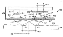
図4は、本発明による実施例400の図であり、光源411を含むナビゲーション装置434を示している。光源411は、光学放射光線412を提供し、これがコリメータ要素413に入射して平行化された光線412’が生成される。但し、光線412’は、平行化させる必要はなく、従って、このコリメータ要素413は、光源411の任意選択要素である。尚、使用する場合には、コリメータ要素413は、例えば、回折又は屈折レンズなどの光学放射光線412を平行化するための適切な光学要素であれば、どのようなものであってもよい。本発明による実施例の中には、光源411が可視波長範囲の光学放射を放出するものも存在するが、本システムは、例えば、シリコン検出器の反応性がピークを示す赤外(IR)領域などのその他の波長範囲の光学放射によって動作するべく構成することも可能である。
FIG. 4 is a diagram of an
光線412’は、領域401として識別されている表面418の一部において光線412”として反射するべく、非垂直入射によって表面418を照射している。領域401の表面の不完全性(表面が光学的に研磨されていない限り、通常、存在するもの)又はその他の不均一性(例:意図的なざらつき)により、個々の光線412”は、反射地点における表面の高さが個々に異なることから結果的に生成される異なる伝播時間を有することになる。この光線ごとに異なる伝播時間により、光線間に位相差が生成され、光線412”上に位相パターンが生成されることになる。
本発明による実施例400は、透過可能な回折格子417を含んでおり、この回折格子は、アレイ画像化装置416による画像取得の前の時点において、位相パターンが変化した光線412”が通過する際に、この光線に対して処理を施すものである。この格子417は、位相パターンが変化した光線412”のそれぞれの少なくとも一部の角度を変化させる。例えば、光線414は、2つの異なる回折次数(光線414’及び414”として示されているもの)に回折し、光線415は、同様に、2つの異なる回折次数(光線415’及び415”として示されているもの)に回折する。この結果、それぞれ光線414’〜415’及び414”〜415”で示されている2つのオフセットされた位相パターンが変化したビームが生成され、これらは、光線414”及び415’(及びこれらの間のすべての光線)が互いの相対的な位相に応じて干渉する(即ち、加算又は減算する)オーバーラップ領域410を定義している。即ち、この回折格子417は、図3D〜図3Eに示されているシアリングプレート(shear plate)の機能を効果的に実行しているのである。
The
回折格子417とアレイ画像化装置416間の合焦要素419は、回折格子417を通過した表面418の画像をアレイ画像化装置416上に合焦する。これにより、インターフェログラムがアレイ画像化装置416上に投影され、このインターフェログラムをアレイ画像化装置が検出して画像信号を生成する。任意選択により、合焦要素419と回折格子417は、単一のモノリシック又は集積構造に組み合わせることができる。図5A〜図5Bは、本発明による装置434と表面418間の異なる相対位置において生成されたインターフェログラムを示す図である。図5Bのインターフェログラム521は、図5Aに示されている表面418上の約6マイクロメートル(μm)の高さの小さな隆起502により、領域401からの反射光線412’上に生成された位相パターンを表す等高線画像520を示している。図5Bに示されているように、インターフェログラム521は、光線412’が表面418において反射する領域401(例えば、通常のコンピュータマウスの場合には、約1mm2〜約4mm2の範囲)に一意に依存している。
A focusing element 419 between the
しかしながら、表面418がナビゲーション装置434に対して移動すると、位相パターンが変化した新しい反射領域に通常一意に依存する別の固有のインターフェログラムが生成されることになろう。例えば、表面418が、図5Aの矢印512によって示されているように、ナビゲーション装置434に対して長手方向に移動すると、新しい領域402が画像化され、結果的に、図5Bに示されているように、等高線画像図520がインターフェログラム521に対して垂直にシフトしたインターフェログラム522が生成されることになる。同様に、等高線画像図520がインターフェログラム521に対して水平にシフトした図5Bのインターフェログラム523は、図5Aの矢印513によって示されているように、装置434が表面418に対して横方向に移動した際に、表面418上に入射する光線412’から生成されることになろう。同様に、等高線画像図520がインターフェログラム521に対して斜めにシフトした図5Bのインターフェログラム524は、図5Aの矢印514によって示されているように、装置434が表面418に対して斜めに移動した際に、上面418上に入射する光線412’から生成されることになろう。
However, movement of the
図5Bに示されているように、連続保存したインターフェログラムを比較することによって相対運動を判定可能であり、縞のパターンの相関計算を使用して相対的な移動の距離と方向を判定することができる。即ち、取得画像は、以前の取得画像と部分的にオーバーラップしている。従って、ナビゲーションソフトウェアのアルゴリズムにより、それぞれの画像上の特定の識別可能な地点を「参照」し、相対的な運動の距離と方向を計算することができる。連続して画像のペアを保存することにより、従来の画像相関アルゴリズムを使用してオーバーラップの特性を判定し、これにより、移動の方向と大きさを導出することができるのである。この操作は、特許文献1に詳述されており、連続した表面画像の比較に基づいた光学ポインティング装置において広く使用されているものである(この場合、表面画像は、表面からの反射光学放射によって生成された影により、従来技術に従って生成されている)。本発明によるインターフェロメトリ技法を使用することにより、例えば、ガラスなどの非常に滑らかな(但し、通常、光学的に研磨されてはいない)表面上における相対移動も判定できるようになる。 As shown in FIG. 5B, relative motion can be determined by comparing successively stored interferograms, and the relative movement distance and direction is determined using a correlation calculation of the fringe pattern. be able to. That is, the acquired image partially overlaps with the previously acquired image. Thus, algorithms in the navigation software can "see" a particular identifiable point on each image and calculate the distance and direction of relative movement. By storing successive pairs of images, conventional image correlation algorithms can be used to determine the nature of the overlap, thereby deriving the direction and magnitude of movement. This operation is described in detail in U.S. Pat. No. 6,037,036 and is widely used in optical pointing devices based on the comparison of successive surface images (where the surface image is reflected by the reflected optical radiation from the surface). The generated shadows are generated according to the prior art). The use of the interferometry technique according to the invention also makes it possible to determine the relative movement on very smooth (but usually not optically polished) surfaces such as, for example, glass.
回折格子417は、例えば、平行板、プリズム、デュアル又は複数格子、又はシアリングプレートの機能を実行する(即ち、シアリングインターフェロメトリを可能にする)あらゆる光学要素によって置換することができる。
図6A〜図6Bは、その上を光学マウス634が移動する固定表面418を備える本発明によるシステム630の図である。光学マウス634は、通常、図1に示されている位相検出器104に類似した位相検出器を含んでいる。光線612(図6B)が(図4に関連して説明したように)表面418から反射し、通常小さな矢印又はポインタの形態で示される一連の連続した位置画像が有線又は無線によってCPU631に送信され、表示画面632上に表示される。通常、この位置計算は、例えば、プロセッサ601及びメモリ602により、マウス634内において実行される。但し、位相検出器からCPU631に生データ(又は、その他の中間データ)を送信し、処理することも可能である。CPU631は、通常、例えば、キーボード633などのユーザー入力装置と相互接続されている。
6A-6B are diagrams of a
図7は、本発明によるシステム740の図であり、この場合には、ナビゲーション装置743が表面742内に格納されており(又は、その一部を構成しており)、位相パターンが変化した光線744は、移動表面741から反射される。装置743は、通常、図1に示されている位相検出器104に類似した位相検出器を含んでいる。尚、装置743と表面741の両方を互いに移動させることも可能であることに留意されたい。又、光学コンポーネント及び設計により、表面741から反射した位相パターンが変化した光線744を装置743内の位相検出器によって取得可能な場合には、これら2つの構造(装置743と表面741)を互いに近接配置させる必要はない。
FIG. 7 is a diagram of a
以上、特定の実施例に関連し、本発明について説明したが、上述の説明に鑑み、当業者には、多くの代替、変更、及び変形が明らかになるであろうことは明白である。従って、本発明には、添付の特許請求の範囲の精神及び範囲に属するそれらその他の代替、変更、及び変形のすべてが包含される。 While the invention has been described with reference to specific embodiments, it is evident that many alternatives, modifications and variations will become apparent to those skilled in the art in light of the above description. Accordingly, the invention includes all such alternatives, modifications, and variations as fall within the spirit and scope of the appended claims.
最後に、本発明の代表的な実施態様を示す。
(実施態様1)
物体に対する移動を検出する光学ナビゲーション装置であって、
前記物体を照射する光学放射の光源と、
前記物体から戻ってきた前記光学放射の位相パターンを検出する検出器とを備え、
前記位相パターンは、前記物体の光学的な不均一性と相関していることを特徴とする光学ナビゲーション装置。
Finally, representative embodiments of the present invention will be described.
(Embodiment 1)
An optical navigation device that detects movement with respect to an object,
A light source of optical radiation for irradiating the object,
A detector for detecting a phase pattern of the optical radiation returned from the object,
The optical navigation device, wherein the phase pattern is correlated with optical non-uniformity of the object.
(実施態様2)
前記位相パターンを、前記検出器が検出する干渉パターンに変換するインターフェロメトリ要素を更に有する実施態様1記載の光学ナビゲーション装置。
(Embodiment 2)
The optical navigation device according to
(実施態様3)
前記インターフェロメトリ要素は、前記物体と前記検出器との間に設けられた、前記位相パターン間に干渉のオーバーラップを生成するためのシアリング要素であることを特徴とする実施態様2記載の光学ナビゲーション装置。
(Embodiment 3)
The optical system according to claim 2, wherein the interferometry element is a shearing element provided between the object and the detector for generating an overlap of interference between the phase patterns. Navigation device.
(実施態様4)
前記ナビゲーション装置は、コンピュータと共に使用するポインティング装置を制御するべく動作し、前記ナビゲーション装置が前記物体に対して移動することを特徴とする実施態様1から3のいずれかに記載の光学ナビゲーション装置。
(Embodiment 4)
4. The optical navigation device according to
(実施態様5)
コンピュータのディスプレイ上の位置ポインタを制御するべく動作可能な手で操作するマウスを備える実施態様4記載の光学ナビゲーション装置。
(Embodiment 5)
The optical navigation device of embodiment 4, comprising a hand operated mouse operable to control a position pointer on a computer display.
(実施態様6)
前記インターフェロメトリ要素は、一連のインターフェログラムを生成するべく動作可能であり、前記ナビゲーション装置と前記物体が互いに対して移動した際に、前記生成されたインターフェログラムのそれぞれは、前記物体の特定部分の構造を示すことを特徴とする実施態様2から5のいずれかに記載の光学ナビゲーション装置。
(Embodiment 6)
The interferometry element is operable to generate a series of interferograms, and when the navigation device and the object move relative to each other, each of the generated interferograms causes The optical navigation device according to any one of Embodiments 2 to 5, wherein a structure of a specific portion is shown.
(実施態様7)
前記検出器によって取得した前記インターフェログラムを処理するべく動作可能な画像プロセッサを更に有し、前記インターフェログラムの第1のものを前記インターフェログラムの中の少なくとも1つの後続のものと相関させ、前記ナビゲーション装置と前記物体の部分間における前記インターフェログラムに対応する相対的な運動を判定する実施態様6に記載の光学ナビゲーション装置。
(Embodiment 7)
An image processor operable to process the interferogram obtained by the detector, correlating a first one of the interferograms with at least one subsequent one of the interferograms The optical navigation device according to embodiment 6, wherein a relative motion corresponding to the interferogram between the navigation device and the part of the object is determined.
(実施態様8)
前記光源は、ダイオードエミッタ、発光ダイオード、マルチモード垂直共振器面発光レーザ、レーザダイオード、及び白色灯のうちのいずれかであることを特徴とする実施態様1から7のいずれかに記載の光学ナビゲーション装置。
(Embodiment 8)
The optical navigation device according to any one of
(実施態様9)
光学ナビゲーション装置と物体間における相対的な移動を検出する方法であって、
前記物体を照射する光学放射ビームを供給する段階と、
前記物体から戻った前記光学放射の位相パターンを検出する検出段階とを有し、
前記位相パターンは、前記物体の光学的な不均一性と相関していることを特徴とする方法。
(Embodiment 9)
A method for detecting a relative movement between an optical navigation device and an object,
Providing an optical radiation beam that illuminates the object;
Detecting a phase pattern of the optical radiation returned from the object.
The method of
(実施態様10)
前記光学放射を供給する段階と前記検出段階は、前記光学ナビゲーション装置内において実行されることを特徴とする実施態様9記載の方法。
(Embodiment 10)
10. The method of embodiment 9, wherein the steps of providing optical radiation and detecting are performed in the optical navigation device.
(実施態様11)
物体に対する移動を検出する光学マウスであって、前記相対的な移動は、コンピュータの画面上の位置ポインタを制御するべく動作し、
それぞれが前記マウスの相対的な位置に対応する前記物体の一部に固有のインターフェログラムを生成する干渉計と、
前記固有のインターフェログラムのペアを前記マウスと前記物体間における相対的な移動に対応する信号に変換する少なくとも1つのプロセッサとを有することを特徴とする光学マウス。
(Embodiment 11)
An optical mouse for detecting movement with respect to an object, wherein the relative movement operates to control a position pointer on a screen of a computer,
Interferometers each generating a unique interferogram on a portion of the object corresponding to a relative position of the mouse;
An optical mouse, comprising: at least one processor that converts the pair of unique interferograms into a signal corresponding to relative movement between the mouse and the object.
(実施態様12)
前記光学放射が前記表面の異なる地点において前記物体の表面から反射されるように前記物体を照射するべく適合された光源を更に有し、それぞれの前記地点からの前記反射光学放射の異なる部分間の位相パターンが、前記反射地点における表面構造によって少なくとも部分的に変化していることを特徴とする実施態様11記載の光学マウス。
(Embodiment 12)
A light source adapted to illuminate the object such that the optical radiation is reflected from a surface of the object at different points on the surface, wherein the light source is adapted to illuminate the object between different portions of the reflected optical radiation from each of the points. 12. The optical mouse of embodiment 11, wherein the phase pattern is at least partially changed by a surface structure at the reflection point.
101、434 光学ナビゲーション装置
102、418 物体
103、411 光源
104、416 検出器
105 画像プロセッサ
107〜108、512〜514 移動
110 光学放射ビーム
112、412” 位相パターン
303、310 シアリング要素
315 干渉のオーバーラップ
417 干渉計
418 物体
502 光学的な不均一性
521〜524 インターフェログラム
601 プロセッサ
630、631、632 コンピュータ
632 ディスプレイ
634、741 光学マウス
101,434 Optical navigation device 102,418 Object 103,411 Light source 104,416
Claims (12)
前記物体を照射する光学放射の光源と、
前記物体から戻ってきた前記光学放射の位相パターンを検出する検出器とを備え、
前記位相パターンは、前記物体の光学的な不均一性と相関していることを特徴とする光学ナビゲーション装置。 An optical navigation device that detects movement with respect to an object,
A light source of optical radiation for irradiating the object,
A detector for detecting a phase pattern of the optical radiation returned from the object,
The optical navigation device, wherein the phase pattern is correlated with optical non-uniformity of the object.
前記物体を照射する光学放射ビームを供給する段階と、
前記物体から戻った前記光学放射の位相パターンを検出する検出段階とを有し、
前記位相パターンは、前記物体の光学的な不均一性と相関していることを特徴とする方法。 A method for detecting a relative movement between an optical navigation device and an object,
Providing an optical radiation beam that illuminates the object;
Detecting a phase pattern of the optical radiation returned from the object.
The method of claim 1, wherein the phase pattern is correlated with optical non-uniformity of the object.
それぞれが前記マウスの相対的な位置に対応する前記物体の一部に固有のインターフェログラムを生成する干渉計と、
前記固有のインターフェログラムのペアを前記マウスと前記物体間における相対的な移動に対応する信号に変換する少なくとも1つのプロセッサとを有することを特徴とする光学マウス。 An optical mouse for detecting movement with respect to an object, wherein the relative movement operates to control a position pointer on a screen of a computer,
Interferometers each generating a unique interferogram on a portion of the object corresponding to a relative position of the mouse;
An optical mouse, comprising: at least one processor that converts the pair of unique interferograms into a signal corresponding to relative movement between the mouse and the object.
A light source adapted to illuminate the object such that the optical radiation is reflected from a surface of the object at different points on the surface, wherein the light source is adapted to illuminate the object between different portions of the reflected optical radiation from each of the points. The optical mouse according to claim 11, wherein the phase pattern is at least partially changed by a surface structure at the reflection point.
Applications Claiming Priority (1)
| Application Number | Priority Date | Filing Date | Title |
|---|---|---|---|
| US10/439,674 US20040227954A1 (en) | 2003-05-16 | 2003-05-16 | Interferometer based navigation device |
Publications (2)
| Publication Number | Publication Date |
|---|---|
| JP2004340950A true JP2004340950A (en) | 2004-12-02 |
| JP2004340950A5 JP2004340950A5 (en) | 2007-05-31 |
Family
ID=33029817
Family Applications (1)
| Application Number | Title | Priority Date | Filing Date |
|---|---|---|---|
| JP2004119296A Withdrawn JP2004340950A (en) | 2003-05-16 | 2004-04-14 | Navigation device using interference |
Country Status (5)
| Country | Link |
|---|---|
| US (1) | US20040227954A1 (en) |
| EP (1) | EP1477888A3 (en) |
| JP (1) | JP2004340950A (en) |
| CN (1) | CN100576154C (en) |
| TW (1) | TWI241516B (en) |
Cited By (1)
| Publication number | Priority date | Publication date | Assignee | Title |
|---|---|---|---|---|
| JP2007517198A (en) * | 2003-12-19 | 2007-06-28 | アバゴ・テクノロジーズ・ジェネラル・アイピー(シンガポール)プライベート・リミテッド | System and method for optical navigation using projected fringe technique |
Families Citing this family (36)
| Publication number | Priority date | Publication date | Assignee | Title |
|---|---|---|---|---|
| US7321359B2 (en) * | 2003-07-30 | 2008-01-22 | Avago Technologies Ecbu Ip (Singapore) Pte. Ltd. | Method and device for optical navigation |
| US7528824B2 (en) * | 2004-09-30 | 2009-05-05 | Microsoft Corporation | Keyboard or other input device using ranging for detection of control piece movement |
| CN100386715C (en) * | 2004-12-14 | 2008-05-07 | 原相科技股份有限公司 | Optical mouse imaging device employing interference imaging principle |
| US8212775B2 (en) | 2005-02-22 | 2012-07-03 | Pixart Imaging Incorporation | Computer input apparatus having a calibration circuit for regulating current to the light source |
| US20060209027A1 (en) * | 2005-03-21 | 2006-09-21 | Pixart Imaging, Inc. | Optical mouse with a light-interfering unit |
| US20060213997A1 (en) * | 2005-03-23 | 2006-09-28 | Microsoft Corporation | Method and apparatus for a cursor control device barcode reader |
| TWM284968U (en) * | 2005-04-13 | 2006-01-01 | Pixart Imaging Inc | Lens module for optical mouse and related optical module and computer input device |
| US7268705B2 (en) * | 2005-06-17 | 2007-09-11 | Microsoft Corporation | Input detection based on speckle-modulated laser self-mixing |
| US7557795B2 (en) * | 2005-06-30 | 2009-07-07 | Microsoft Corporation | Input device using laser self-mixing velocimeter |
| US7898524B2 (en) * | 2005-06-30 | 2011-03-01 | Logitech Europe S.A. | Optical displacement detection over varied surfaces |
| US7399954B2 (en) * | 2005-08-16 | 2008-07-15 | Avago Technologies Ecbu Ip Pte Ltd | System and method for an optical navigation device configured to generate navigation information through an optically transparent layer and to have skating functionality |
| US7283214B2 (en) * | 2005-10-14 | 2007-10-16 | Microsoft Corporation | Self-mixing laser range sensor |
| US7543750B2 (en) * | 2005-11-08 | 2009-06-09 | Microsoft Corporation | Laser velocimetric image scanning |
| US7505033B2 (en) * | 2005-11-14 | 2009-03-17 | Microsoft Corporation | Speckle-based two-dimensional motion tracking |
| US20070109267A1 (en) * | 2005-11-14 | 2007-05-17 | Microsoft Corporation | Speckle-based two-dimensional motion tracking |
| US7746477B1 (en) * | 2006-02-24 | 2010-06-29 | Cypress Semiconductor Corporation | System and method for illuminating and imaging a surface for an optical navigation system |
| US20070242277A1 (en) * | 2006-04-13 | 2007-10-18 | Dolfi David W | Optical navigation in relation to transparent objects |
| US7675020B2 (en) * | 2006-08-28 | 2010-03-09 | Avago Technologies General Ip (Singapore) Pte. Ltd. | Input apparatus and methods having diffuse and specular tracking modes |
| US20080150897A1 (en) * | 2006-12-22 | 2008-06-26 | Timothy Lin | Optical structure for a laser input device |
| US8730167B2 (en) * | 2007-06-28 | 2014-05-20 | Microsoft Corporation | Pointing device with optical positioning on low-diffusive surfaces |
| US20090135140A1 (en) * | 2007-11-27 | 2009-05-28 | Logitech Europe S.A. | System and method for accurate lift-detection of an input device |
| WO2009096618A1 (en) * | 2008-02-01 | 2009-08-06 | Ytel Photonics Inc. | Optical navigation sensor device and optical module, a portable mouse using the same |
| FR2927175B1 (en) * | 2008-02-05 | 2011-02-18 | Altatech Semiconductor | DEVICE FOR INSPECTING SEMICONDUCTOR WAFERS |
| TW200943136A (en) * | 2008-04-03 | 2009-10-16 | Pixart Imaging Inc | Optical pointing device |
| CN101566886B (en) * | 2008-04-21 | 2012-09-26 | 原相科技股份有限公司 | Optical index device |
| US8373110B2 (en) * | 2009-05-26 | 2013-02-12 | Honeywell International Inc. | System and method for linear and angular measurements of a moving object |
| US9703398B2 (en) * | 2009-06-16 | 2017-07-11 | Microsoft Technology Licensing, Llc | Pointing device using proximity sensing |
| US20160025480A1 (en) * | 2014-07-25 | 2016-01-28 | Nikon Corporation | Interferometric level sensor |
| US9817488B2 (en) * | 2015-01-21 | 2017-11-14 | Pixart Imaging (Penang) Sdn. Bhd. | Optical navigation device and related automatic magnification adjusting method |
| US10719144B2 (en) | 2016-05-11 | 2020-07-21 | Otm Technologies Ltd. | Devices and methods for determining relative motion |
| US10268032B2 (en) | 2016-07-07 | 2019-04-23 | The Board Of Regents Of The University Of Texas System | Systems and method for imaging devices with angular orientation indications |
| CN106996753A (en) * | 2017-03-28 | 2017-08-01 | 哈尔滨工业大学深圳研究生院 | Small three dimensional shape measurement system and method based on the micro- fringe projections of LED |
| US11493336B2 (en) * | 2020-06-22 | 2022-11-08 | Pixart Imaging Inc. | Optical navigation device which can determine dirtiness level of cover or fix multi light pattern issue |
| US11523722B2 (en) | 2019-05-28 | 2022-12-13 | Pixart Imaging Inc. | Dirtiness level determining method and electronic device applying the dirtiness level determining method |
| US11933883B2 (en) | 2021-09-24 | 2024-03-19 | Aloft Sensing, Inc. | System and method for self-contained high-precision navigation |
| CN114963994B (en) * | 2022-04-14 | 2023-05-02 | 西安交通大学 | System and grating sensing method for measuring nanometer precision displacement |
Family Cites Families (60)
| Publication number | Priority date | Publication date | Assignee | Title |
|---|---|---|---|---|
| US3881879A (en) * | 1971-10-05 | 1975-05-06 | Reynolds Metals Co | Al-Si-Mg alloy |
| US3881819A (en) * | 1972-11-22 | 1975-05-06 | Nippon Electric Co | Cassette-type hologram graphic tablet |
| US4168906A (en) * | 1978-04-19 | 1979-09-25 | The United States Of America As Represented By The Secretary Of Commerce | Differential Doppler velocity sensor |
| US4294544A (en) * | 1979-08-03 | 1981-10-13 | Altschuler Bruce R | Topographic comparator |
| US4470696A (en) * | 1981-10-14 | 1984-09-11 | Systems Research Laboratories, Inc. | Laser doppler velocimeter |
| US4553842A (en) * | 1983-05-09 | 1985-11-19 | Illinois Tool Works Inc. | Two dimensional optical position indicating apparatus |
| US4664513A (en) * | 1984-09-25 | 1987-05-12 | Cornell Research Foundation, Inc. | Multidimensional vorticity measurement optical probe system |
| US4794384A (en) * | 1984-09-27 | 1988-12-27 | Xerox Corporation | Optical translator device |
| US4857903A (en) * | 1986-05-06 | 1989-08-15 | Summagraphics Corporation | Electro-optical mouse with improved resolution for compensation of optical distortion |
| US4751380A (en) * | 1986-11-25 | 1988-06-14 | Msc Technologies, Inc. | Detector system for optical mouse |
| JP2801360B2 (en) * | 1990-05-21 | 1998-09-21 | キヤノン株式会社 | Doppler speedometer |
| EP0461437B1 (en) * | 1990-05-22 | 1998-07-29 | Canon Kabushiki Kaisha | Information recording apparatus |
| JPH0452559A (en) * | 1990-06-20 | 1992-02-20 | Omron Corp | Velocity measuring apparatus using spatial filter |
| US5103106A (en) * | 1990-09-11 | 1992-04-07 | Moshe Golberstein | Reflective optical instrument for measuring surface reflectance |
| GB9026622D0 (en) * | 1990-12-07 | 1991-01-23 | Ometron Limited | Apparatus for the measurement of surface shape |
| US5729009A (en) * | 1992-10-05 | 1998-03-17 | Logitech, Inc. | Method for generating quasi-sinusoidal signals |
| JP3279116B2 (en) * | 1994-03-22 | 2002-04-30 | 株式会社豊田中央研究所 | Laser Doppler velocimeter |
| IT1272219B (en) * | 1994-04-27 | 1997-06-16 | Siv Soc Italiana Vetro | APPARATUS FOR THE CONTROL OF AN ELECTROCHROMIC WINDOW |
| US5578813A (en) * | 1995-03-02 | 1996-11-26 | Allen; Ross R. | Freehand image scanning device which compensates for non-linear movement |
| US5788804A (en) * | 1995-07-17 | 1998-08-04 | Liba Maschinenfabrik Gmbh | Machine for the production of pre-ready made reinforcement formations |
| US5786804A (en) * | 1995-10-06 | 1998-07-28 | Hewlett-Packard Company | Method and system for tracking attitude |
| US6690474B1 (en) * | 1996-02-12 | 2004-02-10 | Massachusetts Institute Of Technology | Apparatus and methods for surface contour measurement |
| US6256016B1 (en) * | 1997-06-05 | 2001-07-03 | Logitech, Inc. | Optical detection system, device, and method utilizing optical matching |
| US6685313B2 (en) * | 1997-06-30 | 2004-02-03 | Hewlett-Packard Development Company, L.P. | Early transparency detection routine for inkjet printing |
| US6069700A (en) * | 1997-07-31 | 2000-05-30 | The Boeing Company | Portable laser digitizing system for large parts |
| US6220686B1 (en) * | 1998-02-13 | 2001-04-24 | Ascom Hasler Mailing Systems Ag | Measurement of paper speed using laser speckle detection |
| US6219145B1 (en) * | 1998-02-17 | 2001-04-17 | California Institute Of Technology | Interferometric system for precision imaging of vibrating structures |
| US6424407B1 (en) * | 1998-03-09 | 2002-07-23 | Otm Technologies Ltd. | Optical translation measurement |
| CN1548963A (en) * | 1998-03-09 | 2004-11-24 | Otm��������˾ | Optical translational measurement |
| AU6633798A (en) * | 1998-03-09 | 1999-09-27 | Gou Lite Ltd. | Optical translation measurement |
| US6268599B1 (en) * | 1998-12-11 | 2001-07-31 | Avision Inc. | Optical sensor switch system for a scanner |
| US6303924B1 (en) * | 1998-12-21 | 2001-10-16 | Microsoft Corporation | Image sensing operator input device |
| US6442725B1 (en) * | 1999-02-18 | 2002-08-27 | Agilent Technologies, Inc. | System and method for intelligent analysis probe |
| US6222174B1 (en) * | 1999-03-05 | 2001-04-24 | Hewlett-Packard Company | Method of correlating immediately acquired and previously stored feature information for motion sensing |
| US6219143B1 (en) * | 1999-06-16 | 2001-04-17 | Bandag, Incorporated | Method and apparatus for analyzing shearogram images by animation |
| US6564168B1 (en) * | 1999-09-14 | 2003-05-13 | Immersion Corporation | High-resolution optical encoder with phased-array photodetectors |
| US6380529B1 (en) * | 1999-09-29 | 2002-04-30 | Hewlett-Packard Company | Position sensing device having a movable photosensing element |
| US6525306B1 (en) * | 2000-04-25 | 2003-02-25 | Hewlett-Packard Company | Computer mouse with integral digital camera and method for using the same |
| US6642506B1 (en) * | 2000-06-01 | 2003-11-04 | Mitutoyo Corporation | Speckle-image-based optical position transducer having improved mounting and directional sensitivities |
| US6592039B1 (en) * | 2000-08-23 | 2003-07-15 | International Business Machines Corporation | Digital pen using interferometry for relative and absolute pen position |
| WO2002037410A1 (en) * | 2000-11-06 | 2002-05-10 | Koninklijke Philips Electronics N.V. | Method of measuring the movement of an input device. |
| KR20020050787A (en) * | 2000-12-21 | 2002-06-27 | 이형도 | Optical mouse |
| KR100399635B1 (en) * | 2000-12-21 | 2003-09-29 | 삼성전기주식회사 | Optical mouse |
| US6621483B2 (en) * | 2001-03-16 | 2003-09-16 | Agilent Technologies, Inc. | Optical screen pointing device with inertial properties |
| US6774351B2 (en) * | 2001-05-25 | 2004-08-10 | Agilent Technologies, Inc. | Low-power surface for an optical sensor |
| US6903888B2 (en) * | 2002-06-28 | 2005-06-07 | Seagate Technology Llc | Detection of defects embedded in servo pattern on stamper by using scattered light |
| US7050798B2 (en) * | 2002-12-16 | 2006-05-23 | Microsoft Corporation | Input device with user-balanced performance and power consumption |
| US7019733B2 (en) * | 2003-03-31 | 2006-03-28 | Ban Kuan Koay | Optical mouse adapted for use on glass surfaces |
| US7321359B2 (en) * | 2003-07-30 | 2008-01-22 | Avago Technologies Ecbu Ip (Singapore) Pte. Ltd. | Method and device for optical navigation |
| US7116427B2 (en) * | 2003-10-30 | 2006-10-03 | Avago Technologies Ecbu Ip (Singapore) Pte. Ltd. | Low power consumption, broad navigability optical mouse |
| US6934037B2 (en) * | 2003-10-06 | 2005-08-23 | Agilent Technologies, Inc. | System and method for optical navigation using a projected fringe technique |
| US7400317B2 (en) * | 2003-08-29 | 2008-07-15 | Avago Technologies Ecbu Ip Pte Ltd | Finger navigation system using captive surface |
| TWI230359B (en) * | 2003-11-21 | 2005-04-01 | Pacing Technology Co Ltd | Optical image retrieval method |
| US7394454B2 (en) * | 2004-01-21 | 2008-07-01 | Microsoft Corporation | Data input device and method for detecting lift-off from a tracking surface by electrical impedance measurement |
| US7439954B2 (en) * | 2004-04-15 | 2008-10-21 | Logitech Europe S.A. | Multi-light-source illumination system for optical pointing devices |
| US7339575B2 (en) * | 2004-05-25 | 2008-03-04 | Avago Technologies Ecbu Ip Pte Ltd | Optical pointing device with variable focus |
| US7189985B2 (en) * | 2004-10-30 | 2007-03-13 | Avago Technologies General Ip (Singapore) Pte. Ltd. | Tracking separation between an object and a surface using a reducing structure |
| US8081159B2 (en) * | 2005-02-24 | 2011-12-20 | Avago Technologies Ecbu Ip (Singapore) Pte. Ltd. | Programmable lift response for an optical navigation device |
| US7898524B2 (en) * | 2005-06-30 | 2011-03-01 | Logitech Europe S.A. | Optical displacement detection over varied surfaces |
| US7399954B2 (en) * | 2005-08-16 | 2008-07-15 | Avago Technologies Ecbu Ip Pte Ltd | System and method for an optical navigation device configured to generate navigation information through an optically transparent layer and to have skating functionality |
-
2003
- 2003-05-16 US US10/439,674 patent/US20040227954A1/en not_active Abandoned
-
2004
- 2004-01-16 CN CN200410001025A patent/CN100576154C/en not_active Expired - Fee Related
- 2004-01-20 TW TW093101603A patent/TWI241516B/en active
- 2004-01-21 EP EP04001237A patent/EP1477888A3/en not_active Withdrawn
- 2004-04-14 JP JP2004119296A patent/JP2004340950A/en not_active Withdrawn
Cited By (2)
| Publication number | Priority date | Publication date | Assignee | Title |
|---|---|---|---|---|
| JP2007517198A (en) * | 2003-12-19 | 2007-06-28 | アバゴ・テクノロジーズ・ジェネラル・アイピー(シンガポール)プライベート・リミテッド | System and method for optical navigation using projected fringe technique |
| JP4718486B2 (en) * | 2003-12-19 | 2011-07-06 | アバゴ・テクノロジーズ・ジェネラル・アイピー(シンガポール)プライベート・リミテッド | System and method for optical navigation using projected fringe technique |
Also Published As
| Publication number | Publication date |
|---|---|
| TWI241516B (en) | 2005-10-11 |
| CN1551043A (en) | 2004-12-01 |
| CN100576154C (en) | 2009-12-30 |
| US20040227954A1 (en) | 2004-11-18 |
| EP1477888A3 (en) | 2006-06-21 |
| TW200426665A (en) | 2004-12-01 |
| EP1477888A2 (en) | 2004-11-17 |
Similar Documents
| Publication | Publication Date | Title |
|---|---|---|
| JP2004340950A (en) | Navigation device using interference | |
| US7116427B2 (en) | Low power consumption, broad navigability optical mouse | |
| US6934037B2 (en) | System and method for optical navigation using a projected fringe technique | |
| EP1739471B1 (en) | Dual technology (confocal and intererometric) optical profilometer for the inspection and three-dimensional measurement of surfaces | |
| US6882433B2 (en) | Interferometer system of compact configuration | |
| US7046371B2 (en) | Interferometer having a coupled cavity geometry for use with an extended source | |
| JP4879471B2 (en) | Method and apparatus for determining position in response to retroreflective objects | |
| JP2004340950A5 (en) | ||
| US20080174785A1 (en) | Apparatus for the contact-less, interferometric determination of surface height profiles and depth scattering profiles | |
| KR100950351B1 (en) | Fringe pattern discriminator for grazing incidence interferometer | |
| EP3443296B1 (en) | Depth sensing using structured illumination | |
| JPH05503787A (en) | Surface shape measuring device | |
| US20070242277A1 (en) | Optical navigation in relation to transparent objects | |
| JP5428538B2 (en) | Interfering device | |
| US20150354953A1 (en) | Laser triangulation sensor and method of measurement with laser triangulation sensor | |
| KR101539946B1 (en) | Integrated shape measuring apparatus | |
| JP6796780B2 (en) | White interference device and measurement method of white interference device | |
| Lim et al. | A novel one-body dual laser profile based vibration compensation in 3D scanning | |
| Harding et al. | Improved measurement dynamic range for point triangulation probes | |
| JPH01235807A (en) | Depth measuring instrument | |
| JP2004309201A (en) | Optical interferometer | |
| JP3634327B2 (en) | Optical chromatic dispersion spatial coherence tomographic imaging system | |
| JP6761160B2 (en) | Dimension measuring device | |
| TWI252435B (en) | System and method for optical navigation using a projected fringe technique | |
| Quintián et al. | Study of an incremental optical encoder using speckle |
Legal Events
| Date | Code | Title | Description |
|---|---|---|---|
| RD03 | Notification of appointment of power of attorney |
Free format text: JAPANESE INTERMEDIATE CODE: A7423 Effective date: 20060320 |
|
| A711 | Notification of change in applicant |
Free format text: JAPANESE INTERMEDIATE CODE: A711 Effective date: 20070326 |
|
| A521 | Written amendment |
Free format text: JAPANESE INTERMEDIATE CODE: A523 Effective date: 20070409 |
|
| A621 | Written request for application examination |
Free format text: JAPANESE INTERMEDIATE CODE: A621 Effective date: 20070409 |
|
| A761 | Written withdrawal of application |
Free format text: JAPANESE INTERMEDIATE CODE: A761 Effective date: 20070427 |