JP2004337345A - Deodorizing apparatus and deodorizing method - Google Patents
Deodorizing apparatus and deodorizing method Download PDFInfo
- Publication number
- JP2004337345A JP2004337345A JP2003137201A JP2003137201A JP2004337345A JP 2004337345 A JP2004337345 A JP 2004337345A JP 2003137201 A JP2003137201 A JP 2003137201A JP 2003137201 A JP2003137201 A JP 2003137201A JP 2004337345 A JP2004337345 A JP 2004337345A
- Authority
- JP
- Japan
- Prior art keywords
- plasma
- adsorbent
- pulse
- generated
- deodorizing
- Prior art date
- Legal status (The legal status is an assumption and is not a legal conclusion. Google has not performed a legal analysis and makes no representation as to the accuracy of the status listed.)
- Pending
Links
Images


Landscapes
- Treating Waste Gases (AREA)
- Physical Or Chemical Processes And Apparatus (AREA)
- Disinfection, Sterilisation Or Deodorisation Of Air (AREA)
Abstract
Description
【0001】
【発明の属する技術分野】
本発明は、におい成分をプラズマにて分解し、該分解されて生成された物質を吸着材にて吸着することによって脱臭を行う脱臭装置及び脱臭方法に関する。
【0002】
【従来の技術】
近時、プラズマによる脱臭は、他の脱臭方法では除去しにくかった臭気や複合臭気にも有効に働き、安定した脱臭効果を得ることができるという効果を奏する。
【0003】
従来のプラズマ脱臭装置は、例えば非特許文献1に示すように、放電ユニットと吸着・触媒ユニットで構成されている。放電ユニットでは、臭気中でプラズマを発生させ、発生されたプラズマによって臭気は吸着・触媒剤に吸着されやすい状態に変化(活性化)する。即ち、前記プラズマによって活性種が生成されることになる。
【0004】
活性種は、吸着・触媒ユニット内で一旦捕らえられ、前記プラズマによって臭気中に発生する酸化力の強い物質(オゾン(O3)などの酸化ラジカル類)との化学反応(触媒酸化反応)が起こって、無臭の物質となって除去される。
【0005】
また、オゾン除去の目的で出口手前に活性炭吸着体を設けており、同時に有毒ガス残渣も吸着させる機能を持たせている。
【0006】
他の従来例では、例えば非特許文献2に示すように、オゾナイザーによるオゾン脱臭も提案されている。オゾナイザーは、セラミックスに形成された放電電極に適切な高周波・高電圧を印加して、放電電極から沿面放電を発生させ、ここに原料ガス(酸素又は、乾燥空気)を供給することにより、高濃度のオゾンを生成するというものである。この場合も、オゾン除去の目的で出口手前に活性炭吸着体を設けている。
【0007】
【非特許文献1】
日新電機[online]、インターネット<http://kankyou.nissin.co.jp/>
【非特許文献2】
三菱電機グループ[online]、インターネット<http://www.ryomatec.co.jp/jyokin.html>
【0008】
【発明が解決しようとする課題】
しかしながら、従来のプラズマ脱臭装置は、放電ユニットと吸着・触媒ユニットとが分離して構成されていることから、微量成分である悪臭物質は、プラズマ中でラジカル等の活性種との反応で分解するものの、生成された化学的に活性状態の分子が更に反応して別の化学物質になったり(副反応)、場合によっては逆反応を経て元の悪臭物質に戻るおそれがある。
【0009】
プラズマで活性化したガス状物質を効率的に処理することを目的としたPACT(Plasma Assisted Catalytic Technology)では、触媒金属をプラズマ電極としている。従って、電極が触媒活性を発揮するため加熱するか、あるいは紫外光を照射する必要があり、装置が複雑になるという問題がある。
【0010】
しかも、従来のプラズマ発生装置は、高周波あるいは直流による放電が多いことから、大気圧ではエネルギ効率が悪く、損失による発熱を伴う。
【0011】
一方、オゾナイザーを用いた脱臭装置においては、沿面放電の放電領域がセラミックスの表面近傍に限られるため、大流量処理には適さないという問題がある。
【0012】
本発明はこのような問題を考慮してなされたものであり、プラズマから発生した活性種をできるだけ早い時期に吸着安定させることができ、活性種による副反応や逆反応の発生を抑えて、他の有害物質の発生を防止することができる脱臭装置及び脱臭方法を提供することを目的とする。
【0013】
【課題を解決するための手段】
本発明に係る脱臭装置は、プラズマを発生させるプラズマ発生手段と、発生したプラズマによって臭気物質から分解生成された物質を吸着する吸着材とを有し、前記吸着材が前記プラズマの発生領域に直接接触して設置されていることを特徴とする。
【0014】
また、本発明に係る脱臭方法は、発生したプラズマによって生成された物質を吸着する吸着材を、前記プラズマの発生領域に直接接触させて脱臭処理を行うことを特徴とする。
【0015】
通常、プラズマから発生した活性種は、その後に、副反応や逆反応によって他の有害物質に変化するおそれがある。しかし、本発明では、吸着材がプラズマの発生領域に直接接触して設置されていることから、活性種は、副反応や逆反応が起こる前に吸着材に吸着され、吸着物として安定化することになる。
【0016】
このように、本発明においては、プラズマから発生した活性種をできるだけ早い時期に吸着安定させることができ、活性種による副反応や逆反応の発生を抑えて、他の有害物質の発生を防止することができる。
【0017】
また、活性種が吸着材に吸着して吸着物として安定化するということは、吸着材付近の活性種の濃度が、プラズマの発生領域における活性種の濃度よりも低くなっていることを示している。この場合、低濃度の領域を高濃度に移行させるように、即ち、化学平衡に向かってプラズマでの分解反応が促進することになる。
【0018】
また、吸着すべき対象成分は、微量であるため、吸着材の寿命として、実用上問題のない期間を確保することができる。
【0019】
そして、前記吸着材は前記プラズマの発生領域内に設置してもよい。あるいは前記吸着材は、中空部を有し、前記吸着材の前記中空部内において前記プラズマを発生させるようにしてもよい。
【0020】
ところで、高電圧パルスの放電によるプラズマにより、脱臭、殺菌、成膜、有害ガスの分解等を行う技術が適応されるようになってきている(例えば特許第2649340号公報(第8欄第3行〜第41行)、応用物理,第61巻,第10号,1992,第1039頁〜第1043頁「高電圧パルス放電化学気相成長法によるアモルファスシリコン系薄膜の作製」参照)。また、プラズマによる処理を効率よく行うためには、高電圧の極めて幅の狭いパルスを供給することが必要であることがわかってきている(例えば文献「IEEE TRANSACTION ON PLASMIC SCIENCE」,VOL.28,No.2,APRIL 2000,p.434〜442「Improvement of NOx Removal Efficiency Using Short−Width Pulsed Power」参照)。
【0021】
そこで、本発明に係る脱臭装置は、前記プラズマ発生手段において、パルス電界によって前記プラズマを発生させるようにしてもよい。
【0022】
この場合、前記プラズマ発生手段は、大気圧下において前記プラズマを発生させるようにしてもよい。そして、前記プラズマ発生手段にて生成される前記パルス電界は、パルス半値幅が10〜1000nsであることが好ましく、更に好ましくは、パルス半値幅が50〜100nsであるとよい。
【0023】
また、前記プラズマ発生手段にて生成される前記パルス電界は、立ち上がり時における電圧上昇率(dV/dt)が109(V/s)以上であることが好ましく、更に好ましくは1011(V/s)以上であるとよい。
【0024】
前記プラズマ発生手段は、非化石エネルギ源(太陽電池、風力、波力、潮汐、温度差発電、燃料電池、地熱発電等)からの電力供給によって前記パルス電界を発生するようにしてもよい。非化石エネルギ源を使用することにより、本発明に係る脱臭装置の動力源からの二酸化炭素の排出を抑えることができ、環境面でも有効な脱臭装置となる。
【0025】
【発明の実施の形態】
以下、本発明に係る脱臭装置及び脱臭方法の実施の形態例について図1〜図12を参照しながら説明する。
【0026】
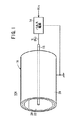
まず、第1の実施の形態に係る脱臭装置10Aは、図1及び図2に示すように、直流入力電圧Vinの供給によって高電圧パルスVL(又は高電圧パルスVLを含む高電圧パルス列Pc)を発生するパルス電源14と、該パルス電源14に接続され、該パルス電源14にて発生された高電圧パルスVL(又は高電圧パルスVLを含む高電圧パルス列Pc)によって放電を発生し、脱臭のための反応を促進させるリアクタ16とを有する。
【0027】
リアクタ16は、パルス電源14に接続された線状電極18と、GNDに接続された筒状電極20とを有し、該筒状電極20の中空部22に線状電極18が挿入されて構成されている。
【0028】
線状電極18は、径が約1mm、長さが約300mmであり、材質はステンレスである。材質としては、その他、インコネル等の耐蝕性導電材料を使用することができる。
【0029】
筒状電極20は、内径が約30mm、外径が約33mm、長さが約300mmであり、材質はステンレスである。材質としては、その他、インコネル等の耐蝕性導電材料を使用することができる。
【0030】
更に、筒状電極20の内壁に筒状の吸着材24が同心円状に配置されている。この吸着材24としては、例えばアルミナやコージェライト等の多孔質セラミックスや、吸着すべき対象成分のみ吸着できるゼオライト、あるいは大きな比表面積を有するγ−Al2O3などが好ましく採用される。吸着材24は、筒状電極20の内壁に対して接着剤によって固着するようにしてもよいし、その他、焼き付けるようにしてもよい。もちろん、金属製の筒状電極20の内壁にガラス質のうわ薬を高温で焼きつけたホーローを用いるようにしてもよい。
【0031】
そして、パルス電源14から出力される高電圧パルスVL(又は高電圧パルスVLを含む高電圧パルス列Pc)としては、図3に示すように、パルス半値幅Tpが10〜1000nsで、立ち上がり時における電圧上昇率(dV/dt)が109(V/s)以上であることが好ましく、更に好ましくは、パルス半値幅Tpが50〜100nsで、立ち上がり時における電圧上昇率(dV/dt)が1011(V/s)以上であるとよい。
【0032】
ここで、この第1の実施の形態に係る脱臭装置10Aの作用について説明する。まず、例えば大気中において臭気成分を含むガスがリアクタ16に導入される。このとき、リアクタ16の線状電極18にパルス電源14から高電圧パルスVLが供給されることによって、筒状電極20の内壁と線状電極18との間で放電が発生し、これによって、臭気成分が導入されている中空部22内でプラズマが発生することになる。このプラズマの発生によって、臭気成分は吸着材24に吸着されやすい状態に変化(活性化)する。即ち、前記プラズマによって活性種が生成されることになる。
【0033】
通常、プラズマから発生した活性種は、その後に、副反応や逆反応によって他の有害物質に変化するおそれがある。
【0034】
しかし、この第1の実施の形態では、内壁に吸着材24が設置された筒状電極20の中空部22に線状電極18を挿入してリアクタ16を構成するようにしているため、吸着材24がプラズマの発生領域26に直接接触して設置された形となる。従って、プラズマによって発生した活性種は、副反応や逆反応が起こる前に吸着材24に吸着され、吸着物として安定化することになる。
【0035】
また、活性種が吸着材24に吸着されて吸着物として安定化するということは、吸着材24付近の活性種の濃度が、プラズマの発生領域26における活性種の濃度よりも低くなっていることを示している。この場合、低濃度の領域を高濃度に移行させるように、即ち、化学平衡に向かってプラズマでの分解反応が促進することになる。
【0036】
また、リアクタ16に導入されるガス中に含まれる臭気成分は微量である。そのため、臭気成分が活性種として分解されて、吸着材24に吸着された場合、吸着時の凝縮によってその量は更に微量になる。このことから、吸着材24の寿命としては、脱臭装置10Aの実用上問題のない耐久期間を見越すことができ、頻繁に取り替える必要がなくなる。
【0037】
ところで、前出の文献(「IEEE TRANSACTION ON PLASMIC SCIENCE」,VOL.28,No.2,APRIL 2000,p.434〜442「Improvement of NOx Removal Efficiency Using Short−Width Pulsed Power」)からもわかるように、プラズマによる処理を効率よく行うためには、高電圧の極めて幅の狭いパルスを供給することが必要である。
【0038】
この第1の実施の形態では、パルス半値幅Tpが10〜1000nsで、立ち上がり時における電圧上昇率(dV/dt)が109(V/s)以上の高電圧パルスによる放電によってプラズマを発生させていることから、臭気成分の分解を高効率に行うことができ、大容量処理も可能となる。
【0039】
この場合、この第1の実施の形態のように、大気圧下において放電を行っても損失が少ないため、ジュール熱の発生が少ない。そのため、高電圧パルス列Pcによって連続的に運転させてもリアクタ16が過熱されることが回避され、安定した状態で稼動することができる。
【0040】
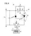
次に、パルス半値幅Tpが10〜1000nsで、立ち上がり時における電圧上昇率(dV/dt)が109(V/s)以上の高電圧パルスを発生させるパルス電源14の具体的な構成について図4〜図5Eを参照しながら説明する。
【0041】
パルス電源14は、図4に示すように、高電圧パルス発生回路30と、駆動信号発生回路32とを有する。
【0042】
高電圧パルス発生回路30は、直流入力電圧Vinが印加される2つの入力端子34及び36間にコンデンサ38が並列に接続され、更に、前記2つの入力端子34及び36間に、インダクタ40、第1の半導体スイッチ42及び第2の半導体スイッチ44が直列に接続されている。なお、インダクタ40の両端のうち、第1の半導体スイッチ42のアノード端子側を一端46と記し、前記一方の入力端子(正極)34側を他端48と記す。
【0043】
この高電圧パルス発生回路30は、また、インダクタ40の他端48と、第1の半導体スイッチ42の制御端子(ゲート)Gとの間に制御端子G側がアノードとなるようにダイオード50が挿入接続され、更に、高電圧パルスVLを必要とするリアクタ16がインダクタ40と並列に接続されている。
【0044】
図4の例では、第2の半導体スイッチ44が他方の入力端子(負極)36側に設けられているが、一方の入力端子(正極)34側に設けても同じ効果をもたらすことは言うまでもない。また、リアクタ16もインダクタ40と並列ではなく、第1の半導体スイッチ42と並列に接続してもよい。
【0045】
第2の半導体スイッチ44は、この図4の例では、アバランシェ形ダイオード52が内蔵された電力用金属酸化半導体電界効果トランジスタ(以下、パワーMOSFETと記す)54を有する。該パワーMOSFET54のゲート端子には、駆動信号発生回路32から駆動信号Vcが供給される。
【0046】
第1の半導体スイッチ42は、この図4の例では、ターンオフ時の電圧上昇率(dV/dt)耐量が極めて大きく、かつ、電圧定格の高いSIサイリスタを用いている。
【0047】
また、この図4の例では、駆動信号発生回路32から出力される駆動信号Vcをパルス列とすることで、高電圧パルス発生回路30からは、複数の高電圧パルスVLが前記駆動信号Vcのパルス列に準じて発生する高電圧パルス列Pcが出力されることになる。
【0048】
この高電圧パルス発生回路30から出力される高電圧パルス列Pcは、図3に示すように、パルス半値幅Tpが10〜1000nsで、立ち上がり時における電圧上昇率(dV/dt)が109(V/s)以上の高電圧パルスVLが、一定周期で出力されるパルス列である。この高電圧パルス列Pcの繰り返し周波数fcは1Hz以上である。更に、この高電圧パルス発生回路30からは、パルス半値幅Tpが50〜100nsで、かつ、立ち上がり時における電圧上昇率(dV/dt)が1011(V/s)以上の高電圧パルスVLが一定周期で出力されるパルス列を出力させることができる。
【0049】
そして、前記駆動信号Vcの出力タイミング、即ち、第2の半導体スイッチ44をオンするタイミングを適宜変更することで、高電圧パルス列Pcの繰り返し周波数fcを変えることができる。なお、駆動信号Vcは、第2の半導体スイッチ44をオンする際には例えば15Vの電圧信号として出力されることになる。
【0050】
ここで、パルス電源14における高電圧パルス発生回路30がリアクタ16に対して高電圧パルスVLを供給する時間経過について、図4の回路図と図5A〜図5Eの動作波形図とを参照しながら説明する。
【0051】
まず、時点t0において、駆動信号発生回路32からパワーMOSFET54のゲート端子に駆動信号Vc(図5E参照)が供給され、パワーMOSFET54がオフからオンになる(図5D参照)。
【0052】
このとき、ダイオード50の逆極性の極めて大きなインピーダンスにより、第1の半導体スイッチ42は、ゲートG及びカソードK間に正に印加される電界効果によりターンオンする。第1の半導体スイッチ42のアノード電流の立ち上がりは、インダクタ40により抑制されるため、電界効果だけでも、正常なターンオンが行われる。なお、ダイオード50と並列に抵抗を接続するか、あるいは他の電源から抵抗を介して第1の半導体スイッチ42のゲートGに積極的にゲート電流を流してもよいことは言うまでもない。
【0053】
このようにして、時点t0で第2の半導体スイッチ44及び第1の半導体スイッチ42が導通すると、インダクタ40に、直流入力電圧Vinとほぼ同じ電圧が印加され、インダクタ40のインダクタンスをLとすると、図5Aに示すように、インダクタ40の電流ILは勾配Vin/Lで時間の経過に伴って直線状に増加する。
【0054】
前記電流ILは、時点t1で電流がIp(=VinT0/L)となり、所望の電磁エネルギ(=LIp2/2)が得られると、駆動信号発生回路32からの駆動信号Vcの供給を停止し、パワーMOSFET54をターンオフさせる(図5E参照)。
【0055】
このとき、前記電流ILの通流経路に存在するインダクタ40以外の図示しない浮遊インダクタンス(主に配線インダクタンス)が大きいと、パワーMOSFET54は瞬時に遮断状態とはならず、若干、電流が流れ続ける時間があり、パワーMOSFET54の出力容量を充電し、ダイオード52のアバランシェ電圧に達すると、該ダイオード52がアバランシェ電圧を持ったまま導通し、大きな損失を発生させる。このため、前記浮遊インダクタンスを極力低減させることにより、ダイオード52がアバランシェまで至らないようにし、ほぼ理想的なターンオフが行われるようにする。
【0056】
パワーMOSFET54がターンオフすることにより、第1の半導体スイッチ42のカソードKからの電流も零、つまり、開放状態となるため、インダクタ40に流れていた電流ILは遮断され、インダクタ40は残留電磁エネルギによって逆誘起電圧を発生させようとするが、ダイオード50が作用し、インダクタ40の電流ILは、第1の半導体スイッチ42のアノードA→第1の半導体スイッチ42のゲートG→ダイオード50のアノード→ダイオード50のカソードの経路に転流する。
【0057】
この場合、ダイオード50が存在する分岐回路の浮遊インダクタンスも極力低くし、転流が短時間で終了するように配慮する必要がある。第1の半導体スイッチ42は、今まで流れていた電流によって、電荷が蓄積されており、この電荷が零となるまでは(ストレージ期間)、第1の半導体スイッチ42のアノードA−ゲートG間は導通状態を維持するため、上記経路の電圧降下は少ない。
【0058】
従って、インダクタ40の逆誘起電圧VLは十分低い値に抑えられるため、時間の短いストレージ期間(図5AのT1)内の前記電流ILの減少はほとんどないが、該期間T1は第1の半導体スイッチ42のゲートGから引き抜かれる電荷量により決まる。そのため、できるだけ大きな電流(図3の例の場合は、アノード電流以上は流せない)を急峻に流し、見かけ上のターンオフ利得を1以下として期間T1を短縮し、インダクタ40の電流ILの減少を極力抑える必要がある。
【0059】
時点t2で第1の半導体スイッチ42の内部に蓄積されていた電荷の引き抜きを完了し、空乏層がカソードK側並びにゲートG側からアノードA側へ広がり、ターンオフ動作を開始する。空乏層は内蔵電位で決まる量により、接合にかかる電圧が増大し、ターンオフが進行するのに従い拡大し、最終的にアノードA近傍に到達する。
【0060】
従って、空乏層による電気容量は、アクティブな電荷が多数存在する飽和状態(導通状態)から、構造で決まる少量の電気容量まで変化していく。インダクタ40の電磁エネルギによる電流が引き続きアノードA→ゲートGに流れ、この空乏層の電気容量を充電する。この充電電圧、つまり、第1の半導体スイッチ42のアノードA−ゲートG間の電圧VAGは、初めは大きい電気容量のため、比較的緩やかに上昇するが、空乏層の広がりとともに急速に上昇していく。
【0061】
時点t3で電流ILが零になると、図5B及び図5Cに示すように、電圧VAG及びVLが最大となり、それぞれVAP及びVLPとなる。この時点で、インダクタ40の電磁エネルギが全て第1の半導体スイッチ42の空乏層の電気容量に移行したことになる。
【0062】
また、この現象は、インダクタ40のインダクタンスと第1の半導体スイッチ42の電気容量とによる共振動作であるため、ほぼインダクタ40の電流ILは余弦波形、第1の半導体スイッチ42のアノードA−ゲートG間の電圧VAGは正弦波形となる。
【0063】
従って、自由に定数を決められるインダクタ40のインダクタンスの値を選ぶことにより、インダクタ40並びに該インダクタ40と並列のリアクタ16に発生する高電圧パルスVLのパルス半値幅Tpをコントロールできる。つまり、第1の半導体スイッチ42の電気容量の等価容量をCとすると、パルス半値幅Tpは、
【0064】
【数1】
となる。
【0066】
時点t3で最大値VAPに充電された第1の半導体スイッチ42の空乏層の電気容量に蓄えられた電荷は、共振現象の継続により、インダクタ40及び蓄積電荷により逆方向に導通状態のダイオード50の経路で放電が始まり、時点t4でダイオード50が逆回復し、非導通になるまで続く。時点t4でインダクタ40及び第1の半導体スイッチ42の空乏層の電気容量にエネルギが残存していれば、このエネルギによる電流は、コンデンサ38→第2の半導体スイッチ44のダイオード52→第1の半導体スイッチ42のカソードK→アノードAの経路で流れる。
【0067】
コンデンサ38に流れる期間T4は回生動作となり、インダクタ40及び第1の半導体スイッチ42の空乏層の電気容量に残存しているエネルギが回生され、運転効率の向上に大きく寄与する。従って、ダイオード50の逆回復時間を極力短縮し、期間T3を短くすることが重要となる。
【0068】
以上の説明ではリアクタ16を抵抗負荷のような線形性のもので説明したが、放電ギャップのような非線形性なものでは、電圧の上昇中に負荷インピーダンスが急減したりして、その後の波形は図5A〜図5Eとは違ったものとなる場合もある。
【0069】
ところで、図4に示すパルス電源14では、第1の半導体スイッチ42のアノードA−カソードK間の電圧はインダクタ40の電圧とほぼ同じであるため、この第1の半導体スイッチ42のアノードA−カソードK間の電圧の耐量以上の電圧を、インダクタ40においてパルス出力させることはできない。
【0070】
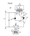
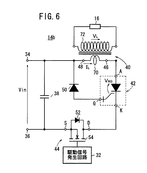
そこで、図6及び図7に示す第1及び第2の変形例に係るパルス電源14a及び14bは、第1の半導体スイッチ42のアノードA−カソードK間電圧の耐量以上の電圧を、インダクタ40においてパルス出力させたい場合に好適となる。
【0071】
まず、第1の変形例に係るパルス電源14aは、図6に示すように、図4に示すパルス電源14とほぼ同様の構成を有するが、インダクタ40が、1次巻線70と、該1次巻線70と磁気的に結合され、かつ、1次巻線70の巻数よりも多い巻数の2次巻線72とを有する点で異なる。
【0072】
一方、第2の変形例に係るパルス電源14bは、図7に示すように、インダクタ40が、1次巻線70と、該1次巻線70に対して直流的に絶縁せずに1次巻線70に加極となるように巻き足した2次巻線72とを有する点で異なる。
【0073】
これら第1及び第2の変形例においては、1次巻線70と2次巻線72間の磁気結合を密にし、漏れ磁束の発生を抑制するために、磁性体コアに巻きつけることが好ましい。
【0074】
そして、1次巻線70の巻数をN1、2次巻線72の巻数をN2とすれば、第1の変形例に係るパルス電源14aの場合には、VAG×(N2/ N1)の高電圧パルスVLをリアクタ16に出力できる。
【0075】
第2の変形例に係るパルス電源14bの場合には、VAG×{(N1+N2)/N1}の高電圧パルスVLをリアクタ16に出力できる。
【0076】
このように、各パルス電源14、14a、14bは、高電圧が印加される半導体スイッチとして1個の第1の半導体スイッチ42でよく、しかも、該第1の半導体スイッチ42のゲート駆動には、通常使用される電子回路によるゲート駆動回路を必要としない。
【0077】
また、各パルス電源14、14a、14bは、高電圧が発生又は供給される部分は、第1の半導体スイッチ42のアノードAとインダクタ40の一端46のみであり、他の回路要素は全て低電圧仕様の回路部品でよい。
【0078】
このことから、例えば図2に示すように、太陽電池等の非化石エネルギ源28からの12V程度の直流入力電圧Vinからでも動作可能であり、部品の電圧定格も数10Vあれば十分である。
【0079】
そして、リアクタ16の線状電極18に高電圧パルスVL(又は高電圧パルスVLを含む高電圧パルス列Pc)が供給されることによって、筒状電極20の内壁と線状電極18との間で放電が発生し、筒状電極20の中空部22においてプラズマが発生することになる。
【0080】
その結果、上述したように、前記プラズマの発生によって、臭気成分が分解されて活性種が生成され、該活性種は、副反応や逆反応が起こる前に吸着材24に吸着され、吸着物として安定化することになる。
【0081】
次に、第1の実施の形態に係る脱臭装置10Aの第1及び第2の変形例について図8及び図9を参照しながら説明する。
【0082】
まず、第1の変形例に係る脱臭装置10Aaは、図8に示すように、上述した第1の実施の形態に係る脱臭装置10Aとほぼ同様の構成を有するが、リアクタ16の筒状電極20と線状電極18との間であって、かつ、これら筒状電極20及び線状電極18に接触しない位置に、中空部22を有する筒状の吸着材24が同心円状に配置されている点で異なる。
【0083】
この場合、線状電極18に高電圧パルスVL(又は高電圧パルスVLを含む高電圧パルス列Pc)が供給されることによって、筒状電極20の内壁と線状電極18との間で放電が発生し、吸着材の中空部22においてプラズマが発生することになる。
【0084】
このプラズマの発生によって、臭気成分が分解されて活性種が生成され、該活性種は、副反応や逆反応が起こる前に吸着材24に吸着され、吸着物として安定化することになる。
【0085】
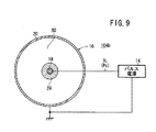
次に、第2の変形例に係る脱臭装置10Abは、図9に示すように、上述した第1の実施の形態に係る脱臭装置10Aとほぼ同様の構成を有するが、リアクタ16の線状電極18の表面に吸着材24が付着され、吸着材24の円周がこれら線状電極18及び筒状電極20と同心円状となっている点で異なる。この場合、吸着材24と筒状電極20間に中空部60が形成されることになる。
【0086】
そして、線状電極18に高電圧パルスVL(又は高電圧パルスVLを含む高電圧パルス列Pc)が供給されることによって、筒状電極20の内壁と線状電極18との間で放電が発生し、筒状電極20と吸着材24との間の中空部60においてプラズマが発生することになる。
【0087】
このプラズマの発生によって、臭気成分が分解されて活性種が生成され、該活性種は、副反応や逆反応が起こる前に吸着材24に吸着され、吸着物として安定化することになる。
【0088】
このように、第1及び第2の変形例に係る脱臭装置10Aa及び10Abにおいても、上述した第1の実施の形態に係る脱臭装置10Aと同様に、プラズマから発生した活性種をできるだけ早い時期に吸着安定させることができ、活性種による副反応や逆反応の発生を抑えて、他の有害物質の発生を防止することができる。
【0089】
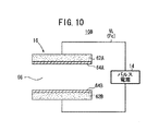
次に、第2の実施の形態に係る脱臭装置10Bについて図10を参照しながら説明する。
【0090】
この第2の実施の形態に係る脱臭装置は、図10に示すように、第1の実施の形態に係る脱臭装置10Aとほぼ同様の構成を有するが、リアクタ16が、互いに対向して配置された2つの平板電極(第1及び第2の平板電極62A及び62B)を有する点で異なる。
【0091】
第1の平板電極62Aと第2の平板電極62B間にパルス電源14が接続されている。
【0092】
更に、第1の平板電極62Aのうち、第2の平板電極62Bと対向する面に平板状の第1の吸着材64Aが固着され、第2の平板電極62Bのうち、第1の平板電極62Aと対向する面に平板状の第2の吸着材64Bが固着されている。
【0093】
まず、例えば大気中において臭気成分を含むガスが第1の吸着材64Aと第2の吸着材64Bとの間の空間66に導入される。このとき、リアクタ16の第1の平板電極62Aに高電圧パルスVL(又は高電圧パルスVLを含む高電圧パルス列Pc)が供給されることによって、第1の平板電極62Aと第2の平板電極62Bとの間で放電が発生し、第1の吸着材64Aと第2の吸着材64Bとの間の空間66においてプラズマが発生することになる。
【0094】
前記プラズマの発生によって、臭気成分が分解されて活性種が生成され、該活性種は、副反応や逆反応が起こる前に第1及び第2の吸着材64A及び64Bに吸着され、吸着物として安定化することになる。
【0095】
次に、第2の実施の形態に係る脱臭装置10Bの変形例について図11及び図12を参照しながら説明する。
【0096】
この変形例に係る脱臭装置10Baは、第1の実施の形態に係る脱臭装置10Aとほぼ同様の構成を有するが、リアクタ16が以下の点で異なる。
【0097】
即ち、図11及び図12に示すように、筒状に形成された吸着材80の上部開口部にメッシュ状の第1の電極82Aがはめ込み固着され、吸着材80の下部開口部にメッシュ状の第2の電極82Bがはめ込み固着されてリアクタ16が構成されている。第1の電極82Aと第2の電極82B間にパルス電源14が接続されている。
【0098】
まず、例えば大気中において臭気成分を含むガスがメッシュ状の第1の電極82Aや第2の電極82Bを通じて吸着材80の中空部84内に導入される。このとき、リアクタ16の第1の電極82Aに高電圧パルスVL(又は高電圧パルスVLを含む高電圧パルス列Pc)が供給されることによって、第1の電極82Aと第2の電極82Bとの間で放電が発生し、吸着材80の中空部84内においてプラズマが発生することになる。
【0099】
前記プラズマの発生によって、臭気成分が分解されて活性種が生成され、該活性種は、副反応や逆反応が起こる前に吸着材80に吸着され、吸着物として安定化することになる。
【0100】
このように、第2の実施の形態に係る脱臭装置10B並びに変形例に係る脱臭装置10Baにおいても、上述した第1の実施の形態に係る脱臭装置10Aと同様に、プラズマから発生した活性種をできるだけ早い時期に吸着安定させることができ、活性種による副反応や逆反応の発生を抑えて、他の有害物質の発生を防止することができる。
【0101】
なお、本発明に係る脱臭装置及び脱臭方法は、上述の実施の形態に限らず、この発明の要旨を逸脱することなく、種々の構成を採り得ることは勿論である。
【0102】
【発明の効果】
以上説明したように、本発明に係る脱臭装置及び脱臭方法によれば、プラズマから発生した活性種をできるだけ早い時期に吸着安定させることができ、活性種による副反応や逆反応の発生を抑えて、他の有害物質の発生を防止することができる。
【図面の簡単な説明】
【図1】第1の実施の形態に係る脱臭装置を示す構成図である。
【図2】第1の実施の形態に係る脱臭装置を示す断面図である。
【図3】パルス電源から出力される高電圧パルス列を示す波形図である。
【図4】パルス電源を示す回路図である。
【図5】図5A〜図5Eは図4に示すパルス電源の各部の電圧および電流の動作波形を説明する図である。
【図6】パルス電源の第1の変形例を示す回路図である。
【図7】パルス電源の第2の変形例を示す回路図である。
【図8】第1の実施の形態に係る脱臭装置の第1の変形例を示す構成図である。
【図9】第1の実施の形態に係る脱臭装置の第2の変形例を示す構成図である。
【図10】第2の実施の形態に係る脱臭装置を示す構成図である。
【図11】第2の実施の形態に係る脱臭装置の変形例を示す構成図である。
【図12】第2の実施の形態に係る脱臭装置のリアクタを一部破断して示す構成図である。
【符号の説明】
10A、10Aa、10Ab、10B、10Ba…脱臭装置
14、14a、14b…パルス電源 16…リアクタ
18…線状電極 20…筒状電極
22、84…中空部 24、80…吸着材
26…プラズマの発生領域 30…高電圧パルス発生回路
32…駆動信号発生回路 62A…第1の平板電極
62B…第2の平板電極 64A…第1の吸着材
64B…第2の吸着材 82A…第1の電極
82B…第2の電極[0001]
TECHNICAL FIELD OF THE INVENTION
The present invention relates to a deodorizing apparatus and a deodorizing method for deodorizing an odor component by decomposing the odor component by plasma and adsorbing the decomposed substance by an adsorbent.
[0002]
[Prior art]
Recently, deodorization by plasma effectively works on odors and complex odors that have been difficult to remove by other deodorization methods, and has an effect that a stable deodorization effect can be obtained.
[0003]
2. Description of the Related Art A conventional plasma deodorizing apparatus includes a discharge unit and an adsorption / catalyst unit, for example, as described in Non-Patent
[0004]
The active species is once caught in the adsorption / catalyst unit and has a strong oxidizing substance (ozone (O 2) generated in the odor by the plasma. 3 ) And a chemical reaction (catalytic oxidation reaction), which is removed as an odorless substance.
[0005]
In addition, an activated carbon adsorbent is provided in front of the outlet for the purpose of removing ozone, and at the same time, has a function of adsorbing toxic gas residues.
[0006]
In another conventional example, as described in Non-Patent Document 2, for example, ozone deodorization using an ozonizer has also been proposed. The ozonizer applies a suitable high frequency and high voltage to a discharge electrode formed on a ceramic to generate a creeping discharge from the discharge electrode, and supply a raw material gas (oxygen or dry air) to the discharge electrode to obtain a high concentration. Ozone is generated. Also in this case, an activated carbon adsorbent is provided just before the outlet for the purpose of removing ozone.
[0007]
[Non-patent document 1]
Nissin Electric [online], Internet <http: // kankyou. nissin. co. jp / >
[Non-patent document 2]
Mitsubishi Electric Group [online], Internet <http: // www. ryomatec. co. jp / jyokin. html>
[0008]
[Problems to be solved by the invention]
However, in the conventional plasma deodorizing apparatus, since the discharge unit and the adsorption / catalyst unit are separated from each other, the malodorous substance, which is a trace component, is decomposed by reaction with active species such as radicals in plasma. However, the generated molecules in a chemically active state may further react to another chemical substance (side reaction), or may return to the original malodorous substance through a reverse reaction in some cases.
[0009]
In PACT (Plasma Assisted Catalytic Technology) for efficiently treating gaseous substances activated by plasma, a catalytic metal is used as a plasma electrode. Therefore, it is necessary to heat or irradiate ultraviolet light in order for the electrode to exhibit catalytic activity, which causes a problem that the apparatus becomes complicated.
[0010]
In addition, the conventional plasma generator has a large amount of high frequency or direct current discharge, and therefore has poor energy efficiency at atmospheric pressure and generates heat due to loss.
[0011]
On the other hand, in the deodorizing apparatus using the ozonizer, there is a problem that the discharge region of the creeping discharge is limited to the vicinity of the surface of the ceramics, so that it is not suitable for the large flow rate treatment.
[0012]
The present invention has been made in view of such a problem, and can stabilize adsorption of active species generated from plasma as early as possible, suppress generation of side reactions and reverse reactions due to active species, and It is an object of the present invention to provide a deodorizing apparatus and a deodorizing method capable of preventing generation of harmful substances.
[0013]
[Means for Solving the Problems]
The deodorizing apparatus according to the present invention has a plasma generating means for generating plasma, and an adsorbent for adsorbing a substance decomposed and generated from an odorant by the generated plasma, wherein the adsorbent is directly in a region where the plasma is generated. It is characterized by being installed in contact.
[0014]
Further, the deodorizing method according to the present invention is characterized in that an adsorbent for adsorbing a substance generated by generated plasma is brought into direct contact with the plasma generation region to perform a deodorizing treatment.
[0015]
Usually, the active species generated from the plasma may be changed to another harmful substance by a side reaction or a reverse reaction. However, in the present invention, since the adsorbent is placed in direct contact with the plasma generation region, the active species is adsorbed by the adsorbent before a side reaction or a reverse reaction occurs, and is stabilized as an adsorbate. Will be.
[0016]
Thus, in the present invention, the active species generated from the plasma can be adsorbed and stabilized as early as possible, and the generation of side reactions and reverse reactions due to the active species is suppressed, and the generation of other harmful substances is prevented. be able to.
[0017]
In addition, the fact that the active species is adsorbed on the adsorbent and is stabilized as an adsorbate indicates that the concentration of the active species near the adsorbent is lower than the concentration of the active species in the plasma generation region. I have. In this case, the decomposition reaction in the plasma is promoted so that the low concentration region is shifted to the high concentration, that is, toward the chemical equilibrium.
[0018]
Further, since the amount of the target component to be adsorbed is very small, a period in which there is no practical problem can be secured as the life of the adsorbent.
[0019]
Further, the adsorbent may be provided in a region where the plasma is generated. Alternatively, the adsorbent may have a hollow portion and generate the plasma in the hollow portion of the adsorbent.
[0020]
By the way, techniques for performing deodorization, sterilization, film formation, decomposition of harmful gas, and the like by using plasma generated by discharge of a high-voltage pulse have been applied (for example, Japanese Patent No. 2649340 (column 8, line 3). To 41), Applied Physics, Vol. 61, No. 10, 1992, pp. 1039 to 1043, "Preparation of amorphous silicon-based thin film by high-voltage pulsed discharge chemical vapor deposition"). It has been found that it is necessary to supply a high-voltage pulse having a very narrow width in order to efficiently perform the plasma treatment (for example, the document “IEEE TRANSACTION ON PLASMIC SCIENCE”, VOL. 28, No. 2, APRIL 2000, pp. 434-442, "Improvement of NOx Removal Efficacy Using Short-Width Pulsed Power").
[0021]
Therefore, in the deodorizing apparatus according to the present invention, the plasma may be generated by the plasma generating means by a pulse electric field.
[0022]
In this case, the plasma generation means may generate the plasma under atmospheric pressure. The pulse electric field generated by the plasma generation means preferably has a pulse half width of 10 to 1000 ns, more preferably 50 to 100 ns.
[0023]
The pulse electric field generated by the plasma generation means has a voltage rise rate (dV / dt) of 10 at the time of rising. 9 (V / s) or more, more preferably 10 11 (V / s) or more.
[0024]
The plasma generating means may generate the pulsed electric field by supplying power from a non-fossil energy source (solar cell, wind power, wave power, tide, temperature difference power generation, fuel cell, geothermal power generation, etc.). By using a non-fossil energy source, the emission of carbon dioxide from the power source of the deodorizing device according to the present invention can be suppressed, and the deodorizing device is also effective in terms of environment.
[0025]
BEST MODE FOR CARRYING OUT THE INVENTION
Hereinafter, embodiments of a deodorizing apparatus and a deodorizing method according to the present invention will be described with reference to FIGS.
[0026]
First, as shown in FIGS. 1 and 2, the
[0027]
The
[0028]
The
[0029]
The
[0030]
Further, a
[0031]
Then, the high voltage pulse V output from the pulse power source 14 L (Or high voltage pulse V L As shown in FIG. 3, the pulse half-width Tp is 10 to 1000 ns and the voltage rise rate (dV / dt) at the time of rising is 10 as shown in FIG. 9 (V / s) or more, more preferably, the pulse half width Tp is 50 to 100 ns, and the voltage rise rate (dV / dt) at the time of rising is 10%. 11 (V / s) or more.
[0032]
Here, the operation of the
[0033]
Usually, the active species generated from the plasma may be changed to another harmful substance by a side reaction or a reverse reaction.
[0034]
However, in the first embodiment, since the
[0035]
The fact that the active species is adsorbed by the adsorbent 24 and is stabilized as an adsorbate means that the concentration of the active species near the adsorbent 24 is lower than the concentration of the active species in the
[0036]
Further, the odor component contained in the gas introduced into the
[0037]
By the way, the above-mentioned document ("IEEE TRANSACTION ON PLASMA SCIENCE", VOL. 28, No. 2, APRIL 2000, pp. 434-442, "Improvement of NOx Removal Efficacy Using Shorty Pow- der is also available from the" Short-hand "as described in the" Short-hand ". In order to perform plasma processing efficiently, it is necessary to supply a high-voltage pulse having a very narrow width.
[0038]
In the first embodiment, the pulse half width Tp is 10 to 1000 ns, and the voltage rise rate (dV / dt) at the time of rising is 10 ns. 9 Since the plasma is generated by the discharge with the high voltage pulse of (V / s) or more, the decomposition of the odor component can be performed with high efficiency, and the large-capacity processing can be performed.
[0039]
In this case, as in the first embodiment, even if the discharge is performed under the atmospheric pressure, the loss is small, and the generation of Joule heat is small. Therefore, even when the
[0040]
Next, the pulse half width Tp is 10 to 1000 ns, and the voltage rise rate (dV / dt) at the time of rising is 10 ns. 9 A specific configuration of the
[0041]
The
[0042]
In the high-voltage
[0043]
In the high-voltage
[0044]
In the example of FIG. 4, the
[0045]
In the example of FIG. 4, the
[0046]
In the example of FIG. 4, the
[0047]
In the example of FIG. 4, the drive signal Vc output from the drive
[0048]
As shown in FIG. 3, the high-voltage pulse train Pc output from the high-voltage
[0049]
The repetition frequency fc of the high-voltage pulse train Pc can be changed by appropriately changing the output timing of the drive signal Vc, that is, the timing of turning on the
[0050]
Here, the high voltage
[0051]
First, at time t 0 5, the drive signal Vc (see FIG. 5E) is supplied from the drive
[0052]
At this time, the
[0053]
Thus, at time t 0 When the
[0054]
The current I L At time t 1 And the current is Ip (= VinT 0 / L) and the desired electromagnetic energy (= LIp 2 / 2) is obtained, the supply of the drive signal Vc from the drive
[0055]
At this time, the current I L If the floating inductance (mainly the wiring inductance) (not shown) other than the
[0056]
When the
[0057]
In this case, it is necessary to reduce the stray inductance of the branch circuit in which the
[0058]
Therefore, the back induced voltage V of the
[0059]
Time t 2 As a result, the extraction of the electric charge stored in the
[0060]
Therefore, the electric capacity of the depletion layer changes from a saturated state (conductive state) where a large number of active charges exist to a small electric capacity determined by the structure. The current due to the electromagnetic energy of the
[0061]
Time t 3 And the current I L Becomes zero, as shown in FIGS. 5B and 5C, AG And V L Is maximum, and V AP And V LP It becomes. At this point, all the electromagnetic energy of the
[0062]
Further, since this phenomenon is a resonance operation due to the inductance of the
[0063]
Therefore, by selecting the value of the inductance of the
[0064]
(Equation 1)
It becomes.
[0066]
Time t 3 At the maximum value V AP The electric charge stored in the depletion layer capacitance of the
[0067]
Period T flowing to
[0068]
In the above description, the
[0069]
By the way, in the
[0070]
Therefore, the
[0071]
First, as shown in FIG. 6, the pulse power supply 14a according to the first modification has substantially the same configuration as the
[0072]
On the other hand, as shown in FIG. 7, the
[0073]
In these first and second modifications, it is preferable to wind the magnetic core around the magnetic core in order to make the magnetic coupling between the primary winding 70 and the secondary winding 72 dense and to suppress the generation of leakage magnetic flux. .
[0074]
If the number of turns of the primary winding 70 is N1 and the number of turns of the secondary winding 72 is N2, then in the case of the pulse power supply 14a according to the first modification, V AG × (N2 / N1) high voltage pulse V L Can be output to the
[0075]
In the case of the
[0076]
As described above, each of the pulse power supplies 14, 14a, and 14b may be a single
[0077]
In each of the pulse power supplies 14, 14a, and 14b, a portion where a high voltage is generated or supplied is only the anode A of the
[0078]
For this reason, as shown in FIG. 2, for example, it is possible to operate from a DC input voltage Vin of about 12 V from a
[0079]
Then, the high voltage pulse V is applied to the
[0080]
As a result, as described above, due to the generation of the plasma, the odor component is decomposed to generate active species, and the active species is adsorbed by the adsorbent 24 before a side reaction or a reverse reaction occurs, and as an adsorbate It will be stabilized.
[0081]
Next, first and second modified examples of the
[0082]
First, the deodorizing device 10Aa according to the first modification has substantially the same configuration as the
[0083]
In this case, the high voltage pulse V L (Or high voltage pulse V L Is supplied, a discharge is generated between the inner wall of the
[0084]
By the generation of the plasma, the odor component is decomposed to generate active species, and the active species is adsorbed by the adsorbent 24 before a side reaction or a reverse reaction occurs, and is stabilized as an adsorbate.
[0085]
Next, the deodorizing device 10Ab according to the second modification has substantially the same configuration as the
[0086]
Then, the high voltage pulse V is applied to the
[0087]
Due to the generation of the plasma, the odor component is decomposed to generate active species, and the active species is adsorbed by the adsorbent 24 before a side reaction or a reverse reaction occurs, and is stabilized as an adsorbate.
[0088]
As described above, also in the deodorizing apparatuses 10Aa and 10Ab according to the first and second modifications, similarly to the
[0089]
Next, a
[0090]
The deodorizing apparatus according to the second embodiment has substantially the same configuration as the
[0091]
The
[0092]
Further, a first plate-
[0093]
First, for example, a gas containing an odor component in the atmosphere is introduced into a
[0094]
Due to the generation of the plasma, the odor component is decomposed to generate active species. The active species is adsorbed by the first and
[0095]
Next, a modification of the
[0096]
The deodorizing device 10Ba according to this modification has substantially the same configuration as the
[0097]
That is, as shown in FIGS. 11 and 12, a mesh-shaped
[0098]
First, for example, a gas containing an odor component in the atmosphere is introduced into the
[0099]
The generation of the plasma decomposes the odor component to generate active species, and the active species is adsorbed by the adsorbent 80 before a side reaction or a reverse reaction occurs, and is stabilized as an adsorbate.
[0100]
As described above, in the
[0101]
In addition, the deodorizing apparatus and the deodorizing method according to the present invention are not limited to the above-described embodiment, but may adopt various configurations without departing from the gist of the present invention.
[0102]
【The invention's effect】
As described above, according to the deodorizing apparatus and the deodorizing method according to the present invention, it is possible to stabilize the adsorption of active species generated from plasma as early as possible, and to suppress the occurrence of side reactions and reverse reactions due to active species. , The generation of other harmful substances can be prevented.
[Brief description of the drawings]
FIG. 1 is a configuration diagram showing a deodorizing device according to a first embodiment.
FIG. 2 is a sectional view showing a deodorizing device according to the first embodiment.
FIG. 3 is a waveform diagram showing a high-voltage pulse train output from a pulse power supply.
FIG. 4 is a circuit diagram showing a pulse power supply.
5A to 5E are diagrams illustrating operation waveforms of voltages and currents of respective parts of the pulse power supply shown in FIG.
FIG. 6 is a circuit diagram showing a first modification of the pulse power supply.
FIG. 7 is a circuit diagram showing a second modification of the pulse power supply.
FIG. 8 is a configuration diagram showing a first modified example of the deodorizing apparatus according to the first embodiment.
FIG. 9 is a configuration diagram showing a second modified example of the deodorizing apparatus according to the first embodiment.
FIG. 10 is a configuration diagram showing a deodorizing device according to a second embodiment.
FIG. 11 is a configuration diagram showing a modified example of the deodorizing device according to the second embodiment.
FIG. 12 is a configuration diagram showing a reactor of a deodorization apparatus according to a second embodiment, partially cut away.
[Explanation of symbols]
10A, 10Aa, 10Ab, 10B, 10Ba ... deodorizer
14, 14a, 14b: pulse power supply 16: reactor
18: Linear electrode 20: Cylindrical electrode
22, 84:
26 ...
32: drive
62B:
64B:
82B ... second electrode
Claims (11)
発生したプラズマによって臭気物質から分解生成された物質を吸着する吸着材とを有し、
前記吸着材が前記プラズマの発生領域に直接接触して設置されていることを特徴とする脱臭装置。Plasma generating means for generating plasma;
An adsorbent that adsorbs substances generated by decomposition from odorous substances by the generated plasma,
The deodorizing device, wherein the adsorbent is provided in direct contact with the plasma generation region.
前記吸着材が前記プラズマの発生領域内に設置されていることを特徴とする脱臭装置。The deodorizing device according to claim 1,
A deodorizing device, wherein the adsorbent is provided in a region where the plasma is generated.
前記吸着材は中空部を有し、
前記吸着材の前記中空部内において前記プラズマが発生することを特徴とする脱臭装置。The deodorizing device according to claim 1,
The adsorbent has a hollow portion,
The deodorizing device, wherein the plasma is generated in the hollow portion of the adsorbent.
前記プラズマ発生手段は、パルス電界によって前記プラズマを発生させることを特徴とする脱臭装置。The deodorizing device according to any one of claims 1 to 3,
The plasma generating means generates the plasma by a pulse electric field.
前記プラズマ発生手段は、大気圧下において前記プラズマを発生させることを特徴とする脱臭装置。In the deodorizing device according to any one of claims 1 to 4,
The deodorizing apparatus, wherein the plasma generating means generates the plasma under atmospheric pressure.
前記プラズマ発生手段にて生成される前記パルス電界は、パルス半値幅が10〜1000nsであることを特徴とする脱臭装置。The deodorizing device according to claim 4 or 5,
The pulse electric field generated by the plasma generating means has a pulse half width of 10 to 1000 ns.
前記パルス電界は、パルス半値幅が50〜100nsであることを特徴とする脱臭装置。The deodorizing device according to claim 6,
The pulse electric field has a pulse half width of 50 to 100 ns.
前記プラズマ発生手段にて生成される前記パルス電界は、立ち上がり時における電圧上昇率(dV/dt)が109(V/s)以上であることを特徴とする脱臭装置。The deodorizing device according to any one of claims 4 to 7,
The deodorizing apparatus, wherein the pulse electric field generated by the plasma generating means has a voltage rise rate (dV / dt) at the time of rising of 10 9 (V / s) or more.
前記電圧上昇率(dV/dt)が1011(V/s)以上であることを特徴とする脱臭装置。The deodorizing device according to claim 8,
The deodorizing device, wherein the voltage rise rate (dV / dt) is 10 11 (V / s) or more.
前記プラズマ発生手段は、非化石エネルギ源からの電力供給によって前記パルス電界を発生することを特徴とする脱臭装置。The deodorizing device according to any one of claims 4 to 9,
The plasma generating means generates the pulse electric field by supplying power from a non-fossil energy source.
Priority Applications (1)
| Application Number | Priority Date | Filing Date | Title |
|---|---|---|---|
| JP2003137201A JP2004337345A (en) | 2003-05-15 | 2003-05-15 | Deodorizing apparatus and deodorizing method |
Applications Claiming Priority (1)
| Application Number | Priority Date | Filing Date | Title |
|---|---|---|---|
| JP2003137201A JP2004337345A (en) | 2003-05-15 | 2003-05-15 | Deodorizing apparatus and deodorizing method |
Publications (1)
| Publication Number | Publication Date |
|---|---|
| JP2004337345A true JP2004337345A (en) | 2004-12-02 |
Family
ID=33526925
Family Applications (1)
| Application Number | Title | Priority Date | Filing Date |
|---|---|---|---|
| JP2003137201A Pending JP2004337345A (en) | 2003-05-15 | 2003-05-15 | Deodorizing apparatus and deodorizing method |
Country Status (1)
| Country | Link |
|---|---|
| JP (1) | JP2004337345A (en) |
Cited By (6)
| Publication number | Priority date | Publication date | Assignee | Title |
|---|---|---|---|---|
| JP2006318814A (en) * | 2005-05-13 | 2006-11-24 | Ngk Insulators Ltd | Discharge lamp driving circuit and driving method of discharge lamp |
| JP2007190498A (en) * | 2006-01-19 | 2007-08-02 | Gunma Univ | Gas treatment method and its device |
| WO2008026712A1 (en) * | 2006-08-29 | 2008-03-06 | Ngk Insulators, Ltd. | Plasma generating method, organic material film etching method, negative ion generating method and oxidizing or nitriding treatment method |
| JP2012521240A (en) * | 2009-03-24 | 2012-09-13 | トゥリ−エアー ディベロップメンツ リミテッド | Improved air decontamination apparatus and method |
| KR101433955B1 (en) * | 2005-07-20 | 2014-08-25 | 알파테크 인터내셔널 리미티드 | Apparatus for air purification and disinfection |
| CN116236994A (en) * | 2023-02-25 | 2023-06-09 | 中国科学院山西煤炭化学研究所 | Reactor for preparing synthesis gas by converting hydrogen sulfide and carbon dioxide mixed gas |
-
2003
- 2003-05-15 JP JP2003137201A patent/JP2004337345A/en active Pending
Cited By (9)
| Publication number | Priority date | Publication date | Assignee | Title |
|---|---|---|---|---|
| JP2006318814A (en) * | 2005-05-13 | 2006-11-24 | Ngk Insulators Ltd | Discharge lamp driving circuit and driving method of discharge lamp |
| JP4500208B2 (en) * | 2005-05-13 | 2010-07-14 | 日本碍子株式会社 | Discharge lamp drive circuit and discharge lamp drive method |
| KR101433955B1 (en) * | 2005-07-20 | 2014-08-25 | 알파테크 인터내셔널 리미티드 | Apparatus for air purification and disinfection |
| JP2007190498A (en) * | 2006-01-19 | 2007-08-02 | Gunma Univ | Gas treatment method and its device |
| WO2008026712A1 (en) * | 2006-08-29 | 2008-03-06 | Ngk Insulators, Ltd. | Plasma generating method, organic material film etching method, negative ion generating method and oxidizing or nitriding treatment method |
| JPWO2008026712A1 (en) * | 2006-08-29 | 2010-01-21 | 日本碍子株式会社 | Plasma generation method, organic material film etching method, negative ion generation method, and oxidation or nitridation method |
| US7914692B2 (en) | 2006-08-29 | 2011-03-29 | Ngk Insulators, Ltd. | Methods of generating plasma, of etching an organic material film, of generating minus ions, of oxidation and nitriding |
| JP2012521240A (en) * | 2009-03-24 | 2012-09-13 | トゥリ−エアー ディベロップメンツ リミテッド | Improved air decontamination apparatus and method |
| CN116236994A (en) * | 2023-02-25 | 2023-06-09 | 中国科学院山西煤炭化学研究所 | Reactor for preparing synthesis gas by converting hydrogen sulfide and carbon dioxide mixed gas |
Similar Documents
| Publication | Publication Date | Title |
|---|---|---|
| Yang et al. | Plasma discharge in liquid: water treatment and applications | |
| US5542967A (en) | High voltage electrical apparatus for removing ecologically noxious substances from gases | |
| KR101553587B1 (en) | Apparatus and method for cleaning air | |
| US5785932A (en) | Catalytic reactor for oxidizing mercury vapor | |
| WO2011079509A1 (en) | Plasma sterilizing-purifying machine and method for air sterilizing and purifying | |
| CN102091514B (en) | Device and method for treating obnoxious gas and industrial VOCs | |
| JP2005222779A (en) | Plasma processing device | |
| Feng et al. | Non-thermal plasma generation by using back corona discharge on catalyst | |
| JP4378592B2 (en) | Control method of discharge generator | |
| Kuroki et al. | Regeneration of honeycomb zeolite by nonthermal plasma desorption of toluene | |
| US6906280B2 (en) | Fast pulse nonthermal plasma reactor | |
| JP2004337345A (en) | Deodorizing apparatus and deodorizing method | |
| JP2006269095A (en) | Plasma generation device | |
| Pemen et al. | An SDBD plasma-catalytic system for on-demand air purification | |
| JP4923364B2 (en) | Reactive gas generator | |
| JP2001276561A (en) | Discharge apparatus equipped with honeycomb structure | |
| JP2005199235A (en) | Photoelectron catalytic purification apparatus and method for removing contaminant | |
| RU2657754C1 (en) | Ion-generating apparatus and method for sterilization and for removing smog | |
| JPH09241007A (en) | Ozone generating method and device | |
| JP5242425B2 (en) | Gas processing equipment | |
| JP2004220985A (en) | Plasma treatment device and plasma treatment method | |
| US7279845B2 (en) | Plasma processing method and apparatus | |
| JP3479002B2 (en) | Air purifier using photocatalyst | |
| KR101194702B1 (en) | Device for removing odorous gas using plasma discharge | |
| JP2004289886A (en) | Pulse power supply unit |
Legal Events
| Date | Code | Title | Description |
|---|---|---|---|
| A621 | Written request for application examination |
Free format text: JAPANESE INTERMEDIATE CODE: A621 Effective date: 20060223 |
|
| A977 | Report on retrieval |
Free format text: JAPANESE INTERMEDIATE CODE: A971007 Effective date: 20080331 |
|
| A131 | Notification of reasons for refusal |
Free format text: JAPANESE INTERMEDIATE CODE: A131 Effective date: 20090519 |
|
| A02 | Decision of refusal |
Free format text: JAPANESE INTERMEDIATE CODE: A02 Effective date: 20091006 |