JP2004309635A - Optical scanner - Google Patents
Optical scanner Download PDFInfo
- Publication number
- JP2004309635A JP2004309635A JP2003100325A JP2003100325A JP2004309635A JP 2004309635 A JP2004309635 A JP 2004309635A JP 2003100325 A JP2003100325 A JP 2003100325A JP 2003100325 A JP2003100325 A JP 2003100325A JP 2004309635 A JP2004309635 A JP 2004309635A
- Authority
- JP
- Japan
- Prior art keywords
- light
- light source
- composite
- optical
- laser diode
- Prior art date
- Legal status (The legal status is an assumption and is not a legal conclusion. Google has not performed a legal analysis and makes no representation as to the accuracy of the status listed.)
- Pending
Links
Images


Classifications
-
- G—PHYSICS
- G02—OPTICS
- G02B—OPTICAL ELEMENTS, SYSTEMS OR APPARATUS
- G02B26/00—Optical devices or arrangements for the control of light using movable or deformable optical elements
- G02B26/08—Optical devices or arrangements for the control of light using movable or deformable optical elements for controlling the direction of light
- G02B26/10—Scanning systems
- G02B26/12—Scanning systems using multifaceted mirrors
- G02B26/123—Multibeam scanners, e.g. using multiple light sources or beam splitters
-
- H—ELECTRICITY
- H01—ELECTRIC ELEMENTS
- H01S—DEVICES USING THE PROCESS OF LIGHT AMPLIFICATION BY STIMULATED EMISSION OF RADIATION [LASER] TO AMPLIFY OR GENERATE LIGHT; DEVICES USING STIMULATED EMISSION OF ELECTROMAGNETIC RADIATION IN WAVE RANGES OTHER THAN OPTICAL
- H01S5/00—Semiconductor lasers
- H01S5/005—Optical components external to the laser cavity, specially adapted therefor, e.g. for homogenisation or merging of the beams or for manipulating laser pulses, e.g. pulse shaping
Abstract
Description
【0001】
【発明の属する技術分野】
本発明は、光走査装置に係り、特に被露光体を複数有するカラープリンタ等の電子写真装置の露光装置に使用するに好適な光走査装置に関する。
【0002】
【従来の技術】
電子写真方式の露光装置は、大きく分類するとレーザダイオードを用いるもいのと発光素子(LED)を用いるものとがある。
発光素子(LED)を用いた露光装置では、被露光体に書き込む画像の画素1ドットに1つのLEDを対応させて露光するようにしており、通常は、多数のLEDを並べたLEDヘッドと呼ばれる光源を使用する。
【0003】
この光源は、LEDが複数個形成されたLEDチップを基板上に並べて多数のLED列を形成するように構成されている。LEDと被露光体の被露光面との間には、光学系を配設して結像面上に光を集光させる(例えば、特許文献1参照)。
【0004】
また、レーザダイオードを用いる露光装置では、一つのレーザビームを、光走査手段を用いて被露光体の露光面上の主走査方向に走査する。
この露光装置では、被露光面上で同一の走査速度及びビーム形状を維持するためにFθレンズを用いる。
【0005】
レーザダイオードから出射したレーザビームは、拡散光であるためにコリメータレンズにより平行光とする。この平行光は、スリット等でビーム形状が制限され、シリンダーレンズでポリゴンミラーの反射面上で副走査方向に集光させる。
次に光走査手段であるポリゴンミラーで主走査方向に走査された光がFθレンズ(またはレンズ群)により被露光体の露光面上に集光され、等速走査される(例えば、特許文献2参照。)。
【0006】
【特許文献1】
特許第3340626号公報
【特許文献2】
特許第3334447号公報
【0007】
【発明が解決しようとする課題】
上述した露光装置のうち発光素子を用いるものでは、露光装置を小型にできる利点がある。しかし、次の欠点を有する。
すなわち、
(1)多数のLEDチップを基板上に精度良く並べることが、必要であること、
(2)回路が複雑であること、
(3)光学系の特性上、LEDチップと被露光体の露光面に至る光学系の距離精度が必要であること、
(4)LEDチップ間の光量のばらつきが大きく、補正が必要であること、
等の欠点が有る。
【0008】
また、レーザダイオードを光源としてポリゴンミラー等で走査する光学系は、以下の利点を有する。
(1)一つの光源を走査するために露光面での光量斑が少ない、
(2)回路が単純である、
(3)光沢的に焦点深度が深いために露光面との距離精度が比較的低い、
等の利点がある。
【0009】
近年、電子写真プリンタは、カラー化が進行している。特にシアン、マゼンタ、イエロー、ブラックの4色の画像を1つの画像にまとめるために従来のブラック/ホワイトに比較して4回画像を形成する必要が有る。
電子写真方式のカラープリンタでは、シングルパス方式とマルチパス方式の2種類が有る。シングルパス方式は1ドラムに1露光装置を組み込み、4色の現像器でそれぞれ現像して中間転写体等に画像を重ねて一括で紙に転写する方式である。
【0010】
マルチパス方式は、4個の現像器と4個の露光装置、4色の現像器を装備し機構的には、従来のブラック/ホワイト方式のプリンタを4個重ねた構造になる。
シングルパス方式は、4回画像を重ねるために印字速度が1/4になり、低速になる欠点がある。また、現像器等を移動する機構が複雑であるが、ドラム、露光装置が一つで構成できる利点がある。
マルチパス方式は、印字速度が速いが、露光装置や感光体が4個必要で複雑になるという欠点が有った。
【0011】
ところで、同一基板上に複数の波長の異なる光束を出射するレーザダイオードを形成した複合光源が従来から各種の装置で使用されている。特に光ピックアップでは、異なる波長の光束を出射する複数のレーザダイオードを有する複合光源を光源として用いて、それぞれ異なる光学系で異なるメディアに対してデータの読み書きが行われていた。
【0012】
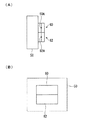
そこで、図3に示すように一つの基板50上に複数のレーザダイオードチップ60、62を半導体プロセスで一体的に形成しコストダウンが図られてきた。因みに図3(A)は、複合電源の正面図、図3(B)はその側面図、60A,62Aは励起発光部である。
このような複合光源を使用する光ピックアップでは、メディアは、一つしか搭載されないためにメディアの種類を認識した後、そのメディアに書き込まれたデータの再生に適応する波長の光束を出射するレーザダイオードを連続発光させ、適応しない波長の光束を出射するレーザダイオードは、消灯している。
【0013】
一方、上述した複合電源を光プリンタで使用する場合は、複数の被露光体(感光ドラム)に異なる画像情報を同時に書き込む必要があるために、波長の異なる複数の光束を出射するレーザダイオードを同時に点灯する必要がある。
しかしながら、図3に示すような同一基板上に形成された隣接する2つのレーザダイオードを同時点灯した場合に、隣接するレーザダイオードのクロストークの影響を受けて発光特性が劣化するものがある。これは、発熱による発光部材料の特性変化や電極等の回路の抵抗値変化により発光特性が変化してしまうなどが原因である。
【0014】
したがって、同一基板上に形成された波長の異なる光束を出射する複数のレーザダイオードを有する複合光源をプリンタの光源として使用する場合に複数のレーザダイオードを同時点灯すると印刷品質が劣化するという問題が有った。
本発明はこのような事情に鑑みてなされたものであり、波長の異なる光束を出射する複数のレーザダイオードを有する複合光源をプリンタの光源として使用し、複数のレーザダイオードを同時点灯した場合にも印字品質を損なうことなく、構成が簡単で、かつ安価なマルチビーム型の光走査装置を提供することを目的とする。
【0015】
【課題を解決するための手段】
上記目的を達成するために、請求項1に記載の発明は、波長の異なるコヒーレント光を出射する複数の光源を近接して配置し各光源の光軸が、略並行に配置され各光軸を中心に広がり角をもって光を照射する複合光源と、該複合光源を構成する各光源の光軸の略中心軸上に配置され前記複合光源からの出射された光束を略平行化するコリメータレンズと、該コリメータレンズから出射した光束を集光するシリンダレンズと、該シリンダレンズにより集光された光束を露光体の露光面における主走査方向に走査するポリゴンミラーとを含む光学系とを有し、前記複合光源を構成する各光源は、基板上に前記各光源の励起発光部が、気体層を挟んで隣接するように配置されることを特徴とする。
【0016】
また、請求項2に記載の発明は、請求項1に記載の光走査装置において、前記複合光源は、複数の異なる光源としてのレーザダイオードチップを前記基板上に接着することにより形成されることを特徴とする。
【0017】
また、請求項3に記載の発明は、請求項1に記載の光走査装置において、前記複合光源を構成する各光源としての各レーザダイオードチップを、基板上に順次、材料を積層させて形成し、前記各レーザダイオードチップの励起発光部間は積層させないうようにしたことを特徴とする。
【0018】
また、請求項4に記載の発明は、請求項2または3のいずれかに記載の光走査装置において、前記複数のレーザダイオードチップの隣接するレーザダイオードチップ間において、そのチップ間隔D2は10μm以上1mm以下であり、前記励起発光部の間隔D1は60μm以上1mm以下である(但し、D1>D2である。)ことを特徴とする。
【0019】
【発明の実施の形態】
以下、本発明の実施形態を、図面を参照して詳細に説明する。本発明の実施形態に係る光走査装置は、波長の異なるコヒーレント光を出射する複数の光源を近接して配置し各光源の光軸が、略並行に配置され各光軸を中心に広がり角をもって光を照射する複合光源と、該複合光源を構成する各光源の光軸の略中心軸上に配置され前記複合光源からの出射された光束を略平行化するコリメータレンズと、該コリメータレンズから出射した光束を集光するシリンダレンズと、該シリンダレンズにより集光された光束を露光体の露光面における主走査方向に走査するポリゴンミラーとを含む光学系とを有し、前記複合光源を構成する各光源は、基板上に前記各光源の励起発光部が、気体層を挟んで隣接するように配置されることを特徴としている。
【0020】
本発明の実施形態に係る光走査装置の構成を図1に示す。図1において、本実施形態に係る光走査装置は、複数(本実施形態では2つ)の異なる波長のコヒーレント光を出射する複合光源10と、コリメータレンズ12と、シリンダレンズ14と、ポリゴンミラー16と、ハーフミラー18と、第1のFθレンズ20と、第1のバンドパスフィルタ22と、第2のFθレンズ24と、ミラー26と、第2のバンドパスフィルタ28とを有している。
【0021】
複合光源10の構成を図2に示す。ここで、図2(A)は複合電源10の正面図、図2(B)は複合電源10の側面図である。複合光源10は、本実施形態では2つの異なる波長のレーザ光(コヒーレント光)を出射するマルチビームレーザダイオードであり、2つの異なる波長(例えば、波長が650nmと780nm)の光束を出射する2つのレーザダイオードチップ110、112(本発明の光源に相当する。)が基板100上に近接して配置されるように構成されている。 111、113は、それぞれ、レーザダイオードチップ110、112における光束を出射する励起発光部である。
【0022】
この2つのレーザダイオードチップ110、112の励起発光部間隔、すなわち、光軸間距離D1は望ましくは、60μm以上1mm以下であり、レーザダイオードチップ110、112のチップ間隔D2は望ましくは、10μm以上1mm以下である(但し、D1>D2である。)。すなわち、複合光源10から出射される複数の光束が一つの光学系で共用化するために、レーザダイオードチップ110、112の光軸間距離D1は及びチップ間隔D2に
このように、基板100上に光源としてのレーザダイオードチップ110、112の励起発光部111、113が、気体層114を挟んで隣接するように配置されている。
2つのレーザダイオードチップ110、112は、基板100上に上記位置関係となるように接着されている。
【0023】
なお、本実施形態では基板100上に2つのレーザダイオードチップ110、112を接着して基板100に搭載しているが、これに限らず、複合光源を構成する各光源としての各レーザダイオードチップを、半導体基板上に順次、材料を積層させて形成し、前記各レーザダイオードチップの励起発光部間は積層させないうようにして複合光源10を構成してもよい。
【0024】
コリメータレンズ12は、複合光源10から出射した光束を平行光にする。
また、シリンダレンズ14は、ポリゴンミラー16の反射面上に光束を集光させる機能を有する。このシリンダレンズ14は、透過する光束に対して被露光体30、32の副走査方向のみパワー(集束機能)を有し、主走査方向にはパワーを有していない。
ポリゴンミラー16は、図示してない駆動手段により一定の角速度で回転駆動され、その回転に伴い、入射された光束を被露光体30、32の被露光面の主走査方向に走査する機能を有している。
【0025】
第1のFθレンズ20は、短波長(650nm)の光束を被露光体30の被露光面に集光し、等速走査するように照射する機能を有する。
また、第2のFθレンズ24は、長波長(780nm)の光束を被露光体32の被露光面に集光し、等速走査するように照射する機能を有する。
また、第1のバンドパスフィルタ22は、短波長(650nm)の光束のみを透過させる機能を有し、第2のバンドパスフィルタ28は、長波長(780nm)の光束のみを透過させる機能を有している。
【0026】
なお、ハーフミラー18と第1のバンドパスフィルタ22、ハーフミラー18と第2のバンドパスフィルタ28は、それぞれ、異なる波長毎に光束を分離する本発明の光学素子に相当する。
また、露光体30、32は、例えば、感光体ドラムであり、図示していない駆動手段により副走査方向に回転駆動されるようになっている。
上記構成において、複合光源10より2つの異なる波長の光束が、それぞれ、図示していない変調手段により、異なる画像等の情報に基づいて強度変調されて出射する。これらの2つの光束は、光軸を中心に広がり角をもって出射する。
【0027】
複合光源10より出射した光束は、コリメータレンズ12により平行光にされ、この平行光となった光束は、シリンダレンズ14により絞り込まれ、ポリゴンミラー16の反射面上に集光される。
ポリゴンミラー16により反射された光束は、ハーフミラー18により二分され、二分された一方の光束は、第1のFθレンズ20、第1のバンドパスフィルタ22を介して被露光体30の被露光面に照射され、ポリゴンミラー16の回転に伴い、被露光体30の被露光面上で主走査方向に走査される。
【0028】
ここで、第1のバンドパスフィルタ22より短波長(650nm)の光束のみが透過するので、短波長(650nm)の光束が第1のFθレンズの作用により被露光体30の被露光面に集光し、この被露光面の主走査方向に等速走査されることとなる。
また、ハーフミラー18で二分された他方の光束は、第2のFθレンズ24、ミラー26、第2のバンドパスフィルタ28を介して被露光体32の被露光面に照射され、ポリゴンミラー16の回転に伴い、被露光体32の被露光面上で主走査方向に走査される。
【0029】
ここで、第2のバンドパスフィルタ22より長波長(780nm)の光束のみが透過するので、長波長(780nm)の光束が第2のFθレンズ24の作用により被露光体30の被露光面に集光し、この被露光面の主走査方向に等速走査されることとなる。
このようにして、被露光体30の被露光面には短波長の光束により、また、被露光体32の被露光面には長波長の光束により、それぞれ異なる画像等の情報が書き込まれることとなる。
【0030】
本発明の実施形態に係る光走査装置によれば、波長の異なる複数の光束を出射する複合光源を光源とし、該光源から出射された各光束を対応する被露光体の主走査方向に走査する光走査装置における光学系を波長の異なる光束で共用化するようにしたので、光走査装置の構成を簡略化することができ、安価な光走査装置を実現することができる。
また、複合光源を構成する複数の各光源(レーザダイオードチップ)は、近接した状態で、かつ基板上に前記各光源の励起発光部が、気体層を挟んで隣接するように配置されているので、隣接する複数の光源を同時点灯しても、クロストークが発生せず、印字品質が劣化することがない。
【0031】
【発明の効果】
以上に説明したように、本発明に係る光走査装置によれば、波長の異なる複数の光束を出射する複合光源を光源とし、該光源から出射された各光束を対応する被露光体の主走査方向に走査する光走査装置における光学系を波長の異なる光束で共用化するようにしたので、光走査装置の構成を簡略化することができ、安価な光走査装置を実現することができる。
【0032】
また、複合光源を構成する複数の各光源(レーザダイオードチップ)は、近接した状態で、かつ基板上に前記各光源の励起発光部が、気体層を挟んで隣接するように配置されているので、隣接する複数の光源を同時点灯しても、クロストークが発生せず、印字品質が劣化することがない。
【図面の簡単な説明】
【図1】本発明の実施形態に係る光走査装置の構成を示す図。
【図2】図1に示した光走査装置における複合電源の構成を示す説明図。
【図3】従来の複合光源の構成を示す説明図。
【符号の説明】
10…複合光源、12…コリメータレンズ、14…シリンダレンズ、16…ポリゴンミラー、18…ハーフミラー、20…第1のFθレンズ、22…第1のバンドパスフィルタ、24…第2のFθレンズ、26…ミラー、28…第2のバンドパスフィルタ、30、32、60、62…被露光体、40…Fθレンズ、42…波長補正レンズ、50…ダイクロイックミラー、100…基板、110、112…レーザダイオードチップ、111、113…励起発光部、114…気体層[0001]
TECHNICAL FIELD OF THE INVENTION
The present invention relates to an optical scanning device, and more particularly to an optical scanning device suitable for use in an exposure device of an electrophotographic apparatus such as a color printer having a plurality of objects to be exposed.
[0002]
[Prior art]
Electrophotographic exposure apparatuses can be broadly classified into those using a laser diode and those using a light emitting element (LED).
In an exposure apparatus using a light emitting element (LED), one LED is exposed to one dot of a pixel of an image to be written on an object to be exposed, and is usually called an LED head in which many LEDs are arranged. Use a light source.
[0003]
This light source is configured such that a large number of LED rows are formed by arranging LED chips on which a plurality of LEDs are formed on a substrate. An optical system is provided between the LED and the surface to be exposed of the object to be exposed, and the light is focused on the image forming surface (for example, see Patent Document 1).
[0004]
In an exposure apparatus using a laser diode, one laser beam is scanned in the main scanning direction on an exposure surface of an object to be exposed using an optical scanning unit.
In this exposure apparatus, an Fθ lens is used to maintain the same scanning speed and beam shape on the surface to be exposed.
[0005]
Since the laser beam emitted from the laser diode is diffused light, it is converted into parallel light by a collimator lens. The beam shape of the parallel light is limited by a slit or the like, and is condensed in the sub-scanning direction on the reflection surface of the polygon mirror by a cylinder lens.
Next, light scanned in the main scanning direction by a polygon mirror serving as an optical scanning unit is condensed on an exposure surface of an object to be exposed by an Fθ lens (or lens group), and is scanned at a constant speed (for example, see Patent Document 2). reference.).
[0006]
[Patent Document 1]
Japanese Patent No. 3340626 [Patent Document 2]
Japanese Patent No. 3333447
[Problems to be solved by the invention]
Among the above-described exposure apparatuses, those using a light emitting element have an advantage that the exposure apparatus can be downsized. However, it has the following disadvantages.
That is,
(1) It is necessary to arrange a large number of LED chips on a substrate with high accuracy;
(2) the circuit is complicated;
(3) Due to the characteristics of the optical system, it is necessary to have a distance accuracy between the LED chip and the exposed surface of the object to be exposed,
(4) the variation in the amount of light between the LED chips is large and correction is required;
And the like.
[0008]
An optical system that scans with a polygon mirror or the like using a laser diode as a light source has the following advantages.
(1) There is little unevenness in the amount of light on the exposure surface because one light source is scanned.
(2) The circuit is simple,
(3) the distance accuracy with respect to the exposed surface is relatively low because of the glossy depth of focus;
There are advantages such as.
[0009]
In recent years, colorization of electrophotographic printers has been progressing. In particular, it is necessary to form an image four times in comparison with the conventional black / white in order to combine four color images of cyan, magenta, yellow and black into one image.
There are two types of electrophotographic color printers, a single-pass type and a multi-pass type. The single-pass method is a method in which one exposure device is incorporated in one drum, developed by four color developing units, and an image is superimposed on an intermediate transfer member or the like and transferred collectively to paper.
[0010]
The multi-pass system has four developing units, four exposing devices, and four-color developing units, and has a structure in which four conventional black / white type printers are stacked mechanically.
The single-pass method has a drawback that the printing speed is reduced to 1/4 and the speed is reduced because images are superimposed four times. Although the mechanism for moving the developing device and the like is complicated, there is an advantage that the drum and the exposure device can be constituted by one.
Although the multi-pass method has a high printing speed, it has a drawback that it requires four exposure devices and photoconductors and is complicated.
[0011]
By the way, a complex light source in which a laser diode that emits a plurality of light beams having different wavelengths on the same substrate is conventionally used in various devices. In particular, in an optical pickup, data reading and writing are performed on different media by different optical systems using a composite light source having a plurality of laser diodes that emit light beams having different wavelengths as a light source.
[0012]
Therefore, as shown in FIG. 3, a plurality of
In an optical pickup using such a composite light source, since only one medium is mounted, a laser diode that recognizes the type of the medium and emits a light beam having a wavelength suitable for reproducing data written on the medium. Are continuously emitted, and the laser diode that emits a light beam of a wavelength that is not adapted is turned off.
[0013]
On the other hand, when the above-described composite power supply is used in an optical printer, it is necessary to simultaneously write different image information on a plurality of exposure targets (photosensitive drums). It needs to be lit.
However, when two adjacent laser diodes formed on the same substrate as shown in FIG. 3 are simultaneously turned on, there is a case where light emission characteristics are deteriorated due to the influence of crosstalk between the adjacent laser diodes. This is because light emission characteristics change due to a change in characteristics of a light emitting portion material due to heat generation or a change in resistance of a circuit such as an electrode.
[0014]
Therefore, when a composite light source having a plurality of laser diodes that emit light beams having different wavelengths and formed on the same substrate is used as a light source of a printer, there is a problem that if a plurality of laser diodes are simultaneously turned on, print quality deteriorates. Was.
The present invention has been made in view of such circumstances, and a composite light source having a plurality of laser diodes that emit light beams having different wavelengths is used as a light source of a printer, and even when a plurality of laser diodes are simultaneously turned on. It is an object of the present invention to provide an inexpensive multi-beam optical scanning device that has a simple configuration and does not impair printing quality.
[0015]
[Means for Solving the Problems]
In order to achieve the above object, the invention according to claim 1 arranges a plurality of light sources that emit coherent light beams having different wavelengths close to each other, the optical axes of the light sources are arranged substantially in parallel, and the optical axes are aligned. A composite light source that irradiates light with a divergence angle at the center, and a collimator lens that is disposed on a substantially central axis of an optical axis of each light source that constitutes the composite light source and that substantially collimates a light flux emitted from the composite light source, An optical system including a cylinder lens that condenses the light beam emitted from the collimator lens, and a polygon mirror that scans the light beam condensed by the cylinder lens in the main scanning direction on the exposure surface of the exposure body; Each light source constituting the composite light source is characterized in that the excitation light emitting portions of the respective light sources are arranged on a substrate so as to be adjacent to each other with a gas layer interposed therebetween.
[0016]
According to a second aspect of the present invention, in the optical scanning device according to the first aspect, the composite light source is formed by bonding a plurality of laser diode chips as different light sources on the substrate. Features.
[0017]
According to a third aspect of the present invention, in the optical scanning device according to the first aspect, each laser diode chip as each light source constituting the composite light source is formed by sequentially laminating materials on a substrate. In addition, the laser diode chips are not stacked between the excitation light emitting portions.
[0018]
According to a fourth aspect of the present invention, in the optical scanning device according to the second or third aspect, a chip interval D2 between the laser diode chips adjacent to the plurality of laser diode chips is 10 μm or more and 1 mm. The distance D1 between the excitation light emitting portions is 60 μm or more and 1 mm or less (where D1> D2).
[0019]
BEST MODE FOR CARRYING OUT THE INVENTION
Hereinafter, embodiments of the present invention will be described in detail with reference to the drawings. In the optical scanning device according to the embodiment of the present invention, a plurality of light sources that emit coherent light beams having different wavelengths are arranged close to each other, and the optical axes of the respective light sources are arranged substantially in parallel and have a divergence angle around each optical axis. A composite light source for irradiating light, a collimator lens disposed on a substantially central axis of an optical axis of each light source constituting the composite light source, and substantially collimating a light beam emitted from the composite light source; An optical system including a cylinder lens for condensing the light beam obtained by the above-mentioned method, and a polygon mirror for scanning the light beam condensed by the cylinder lens in the main scanning direction on the exposure surface of the exposure body to constitute the composite light source. Each light source is characterized in that the excitation light emitting portions of the respective light sources are arranged on a substrate so as to be adjacent to each other with a gas layer interposed therebetween.
[0020]
FIG. 1 shows a configuration of an optical scanning device according to an embodiment of the present invention. In FIG. 1, an optical scanning device according to the present embodiment includes a composite
[0021]
FIG. 2 shows the configuration of the composite
[0022]
The distance between the excited light emitting portions of the two
The two
[0023]
In the present embodiment, the two
[0024]
The
Further, the
The
[0025]
The
The
The
[0026]
The
The
In the above configuration, light beams of two different wavelengths from the composite
[0027]
The light beam emitted from the composite
The light beam reflected by the
[0028]
Here, since only a light beam having a short wavelength (650 nm) is transmitted through the
The other light beam split by the
[0029]
Here, since only a light beam having a long wavelength (780 nm) is transmitted from the
In this way, different information such as images is written on the exposed surface of the exposed
[0030]
According to the optical scanning device according to the embodiment of the present invention, a composite light source that emits a plurality of light beams having different wavelengths is used as a light source, and each light beam emitted from the light source is scanned in a main scanning direction of a corresponding object to be exposed. Since the optical system in the optical scanning device is shared by light beams having different wavelengths, the configuration of the optical scanning device can be simplified, and an inexpensive optical scanning device can be realized.
Further, since the plurality of light sources (laser diode chips) constituting the composite light source are arranged in close proximity and on the substrate, the excitation light emitting portions of the respective light sources are arranged adjacent to each other with a gas layer interposed therebetween. Even when a plurality of adjacent light sources are turned on at the same time, no crosstalk occurs and the print quality does not deteriorate.
[0031]
【The invention's effect】
As described above, according to the optical scanning device of the present invention, a composite light source that emits a plurality of light beams having different wavelengths is used as a light source, and each light beam emitted from the light source is main-scanned on a corresponding exposure target. Since the optical system in the optical scanning device that scans in the direction is shared by light beams having different wavelengths, the configuration of the optical scanning device can be simplified, and an inexpensive optical scanning device can be realized.
[0032]
Further, since the plurality of light sources (laser diode chips) constituting the composite light source are arranged in close proximity and on the substrate, the excitation light emitting portions of the respective light sources are arranged adjacent to each other with a gas layer interposed therebetween. Even when a plurality of adjacent light sources are turned on at the same time, no crosstalk occurs and the print quality does not deteriorate.
[Brief description of the drawings]
FIG. 1 is a diagram showing a configuration of an optical scanning device according to an embodiment of the present invention.
FIG. 2 is an explanatory diagram showing a configuration of a composite power supply in the optical scanning device shown in FIG.
FIG. 3 is an explanatory diagram showing a configuration of a conventional composite light source.
[Explanation of symbols]
10 composite light source, 12 collimator lens, 14 cylinder lens, 16 polygon mirror, 18 half mirror, 20 first Fθ lens, 22 first bandpass filter, 24 second Fθ lens, 26 mirror, 28 second bandpass filter, 30, 32, 60, 62 exposure target, 40 Fθ lens, 42 wavelength correction lens, 50 dichroic mirror, 100 substrate, 110, 112 laser Diode chip, 111, 113 ... excitation light emitting part, 114 ... gas layer
Claims (4)
該複合光源を構成する各光源の光軸の略中心軸上に配置され前記複合光源からの出射された光束を略平行化するコリメータレンズと、該コリメータレンズから出射した光束を集光するシリンダレンズと、該シリンダレンズにより集光された光束を露光体の露光面における主走査方向に走査するポリゴンミラーとを含む光学系とを有し、
前記複合光源を構成する各光源は、基板上に前記各光源の励起発光部が、気体層を挟んで隣接するように配置されることを特徴とする光走査装置。A composite light source that arranges a plurality of light sources that emit coherent light beams having different wavelengths in close proximity, and the optical axes of the light sources are arranged substantially in parallel and emit light with a divergence angle around each optical axis,
A collimator lens disposed substantially on the central axis of the optical axis of each light source that constitutes the composite light source, for collimating the light beam emitted from the composite light source, and a cylinder lens for condensing the light beam emitted from the collimator lens And an optical system including a polygon mirror that scans the light beam condensed by the cylinder lens in the main scanning direction on the exposure surface of the exposure body,
An optical scanning device, wherein each of the light sources constituting the composite light source is arranged on a substrate such that excitation light emitting portions of the respective light sources are adjacent to each other with a gas layer interposed therebetween.
Priority Applications (3)
| Application Number | Priority Date | Filing Date | Title |
|---|---|---|---|
| JP2003100325A JP2004309635A (en) | 2003-04-03 | 2003-04-03 | Optical scanner |
| KR1020030072991A KR100584582B1 (en) | 2003-04-03 | 2003-10-20 | Light scanning unit |
| US10/798,861 US6922269B2 (en) | 2003-04-03 | 2004-03-12 | Light scanning unit |
Applications Claiming Priority (1)
| Application Number | Priority Date | Filing Date | Title |
|---|---|---|---|
| JP2003100325A JP2004309635A (en) | 2003-04-03 | 2003-04-03 | Optical scanner |
Publications (1)
| Publication Number | Publication Date |
|---|---|
| JP2004309635A true JP2004309635A (en) | 2004-11-04 |
Family
ID=33095233
Family Applications (1)
| Application Number | Title | Priority Date | Filing Date |
|---|---|---|---|
| JP2003100325A Pending JP2004309635A (en) | 2003-04-03 | 2003-04-03 | Optical scanner |
Country Status (3)
| Country | Link |
|---|---|
| US (1) | US6922269B2 (en) |
| JP (1) | JP2004309635A (en) |
| KR (1) | KR100584582B1 (en) |
Families Citing this family (3)
| Publication number | Priority date | Publication date | Assignee | Title |
|---|---|---|---|---|
| US8085678B2 (en) * | 2004-10-13 | 2011-12-27 | Qualcomm Incorporated | Media (voice) playback (de-jitter) buffer adjustments based on air interface |
| US7802901B2 (en) * | 2007-09-25 | 2010-09-28 | Cree, Inc. | LED multi-chip lighting units and related methods |
| CN101848299B (en) * | 2009-03-26 | 2014-04-16 | 海德堡印刷机械股份公司 | Device for imaging a flat object |
Family Cites Families (2)
| Publication number | Priority date | Publication date | Assignee | Title |
|---|---|---|---|---|
| JP3149402B2 (en) * | 1999-02-09 | 2001-03-26 | 株式会社ナカニシ | Medical lighting equipment |
| WO2004008023A1 (en) * | 2002-07-11 | 2004-01-22 | Sharp Kabushiki Kaisha | Light guide device and display device |
-
2003
- 2003-04-03 JP JP2003100325A patent/JP2004309635A/en active Pending
- 2003-10-20 KR KR1020030072991A patent/KR100584582B1/en not_active IP Right Cessation
-
2004
- 2004-03-12 US US10/798,861 patent/US6922269B2/en not_active Expired - Fee Related
Also Published As
| Publication number | Publication date |
|---|---|
| US6922269B2 (en) | 2005-07-26 |
| KR100584582B1 (en) | 2006-05-30 |
| KR20040087247A (en) | 2004-10-13 |
| US20040196519A1 (en) | 2004-10-07 |
Similar Documents
| Publication | Publication Date | Title |
|---|---|---|
| EP1361069B1 (en) | Color laser printer | |
| US20100124434A1 (en) | Light source device, optical scanning device, and image forming apparatus | |
| JP2005099315A (en) | Scanning optical device and image forming apparatus | |
| US5956070A (en) | Color xerographic printer with multiple linear arrays of surface emitting lasers with dissimilar polarization states and dissimilar wavelengths | |
| EP2360508B1 (en) | Multiple-source multiple-beam polarized laser scanning system | |
| EP2253987A1 (en) | Multiple integrated multi-beam laser scanning system | |
| US7151624B2 (en) | Light scanning unit | |
| JP2004309635A (en) | Optical scanner | |
| JP2004163740A (en) | Multiple beam scanning optical device and image forming apparatus using the same | |
| JP2010241078A (en) | Exposure device and image forming apparatus | |
| JP2004013021A (en) | Light source device, light source module, optical scanner, and image forming device | |
| US7202986B2 (en) | Light scanning unit | |
| KR100584581B1 (en) | Light scanning unit | |
| US20040056185A1 (en) | Light scanning device of laser printer | |
| US7256812B2 (en) | Laser exposing apparatus | |
| EP0781663B1 (en) | Color xerographic printer with multiple linear arrays of surface emitting lasers with dissimilar wavelengths | |
| JP2006039278A (en) | Scanning lens and scanning optical apparatus having the same | |
| JPH1148521A (en) | Optical printer head | |
| KR20050110486A (en) | Light scanning apparatus |
Legal Events
| Date | Code | Title | Description |
|---|---|---|---|
| A621 | Written request for application examination |
Free format text: JAPANESE INTERMEDIATE CODE: A621 Effective date: 20040901 |
|
| RD02 | Notification of acceptance of power of attorney |
Free format text: JAPANESE INTERMEDIATE CODE: A7422 Effective date: 20060120 |
|
| A521 | Written amendment |
Free format text: JAPANESE INTERMEDIATE CODE: A523 Effective date: 20060124 |
|
| RD04 | Notification of resignation of power of attorney |
Free format text: JAPANESE INTERMEDIATE CODE: A7424 Effective date: 20060127 |
|
| A977 | Report on retrieval |
Free format text: JAPANESE INTERMEDIATE CODE: A971007 Effective date: 20070115 |
|
| A131 | Notification of reasons for refusal |
Free format text: JAPANESE INTERMEDIATE CODE: A131 Effective date: 20070123 |
|
| A02 | Decision of refusal |
Free format text: JAPANESE INTERMEDIATE CODE: A02 Effective date: 20070626 |