EP0781663B1 - Color xerographic printer with multiple linear arrays of surface emitting lasers with dissimilar wavelengths - Google Patents
Color xerographic printer with multiple linear arrays of surface emitting lasers with dissimilar wavelengths Download PDFInfo
- Publication number
- EP0781663B1 EP0781663B1 EP19960308991 EP96308991A EP0781663B1 EP 0781663 B1 EP0781663 B1 EP 0781663B1 EP 19960308991 EP19960308991 EP 19960308991 EP 96308991 A EP96308991 A EP 96308991A EP 0781663 B1 EP0781663 B1 EP 0781663B1
- Authority
- EP
- European Patent Office
- Prior art keywords
- wavelength
- printer
- array
- photoreceptor
- separation means
- Prior art date
- Legal status (The legal status is an assumption and is not a legal conclusion. Google has not performed a legal analysis and makes no representation as to the accuracy of the status listed.)
- Expired - Lifetime
Links
Images


Classifications
-
- B—PERFORMING OPERATIONS; TRANSPORTING
- B41—PRINTING; LINING MACHINES; TYPEWRITERS; STAMPS
- B41J—TYPEWRITERS; SELECTIVE PRINTING MECHANISMS, i.e. MECHANISMS PRINTING OTHERWISE THAN FROM A FORME; CORRECTION OF TYPOGRAPHICAL ERRORS
- B41J2/00—Typewriters or selective printing mechanisms characterised by the printing or marking process for which they are designed
- B41J2/435—Typewriters or selective printing mechanisms characterised by the printing or marking process for which they are designed characterised by selective application of radiation to a printing material or impression-transfer material
- B41J2/447—Typewriters or selective printing mechanisms characterised by the printing or marking process for which they are designed characterised by selective application of radiation to a printing material or impression-transfer material using arrays of radiation sources
- B41J2/45—Typewriters or selective printing mechanisms characterised by the printing or marking process for which they are designed characterised by selective application of radiation to a printing material or impression-transfer material using arrays of radiation sources using light-emitting diode [LED] or laser arrays
-
- G—PHYSICS
- G06—COMPUTING OR CALCULATING; COUNTING
- G06K—GRAPHICAL DATA READING; PRESENTATION OF DATA; RECORD CARRIERS; HANDLING RECORD CARRIERS
- G06K15/00—Arrangements for producing a permanent visual presentation of the output data, e.g. computer output printers
- G06K15/02—Arrangements for producing a permanent visual presentation of the output data, e.g. computer output printers using printers
- G06K15/12—Arrangements for producing a permanent visual presentation of the output data, e.g. computer output printers using printers by photographic printing, e.g. by laser printers
- G06K15/1238—Arrangements for producing a permanent visual presentation of the output data, e.g. computer output printers using printers by photographic printing, e.g. by laser printers simultaneously exposing more than one point
- G06K15/1257—Arrangements for producing a permanent visual presentation of the output data, e.g. computer output printers using printers by photographic printing, e.g. by laser printers simultaneously exposing more than one point on more than one main scanning line
- G06K15/1271—Arrangements for producing a permanent visual presentation of the output data, e.g. computer output printers using printers by photographic printing, e.g. by laser printers simultaneously exposing more than one point on more than one main scanning line by light beam splitting
-
- G—PHYSICS
- G06—COMPUTING OR CALCULATING; COUNTING
- G06K—GRAPHICAL DATA READING; PRESENTATION OF DATA; RECORD CARRIERS; HANDLING RECORD CARRIERS
- G06K15/00—Arrangements for producing a permanent visual presentation of the output data, e.g. computer output printers
- G06K15/02—Arrangements for producing a permanent visual presentation of the output data, e.g. computer output printers using printers
- G06K15/12—Arrangements for producing a permanent visual presentation of the output data, e.g. computer output printers using printers by photographic printing, e.g. by laser printers
- G06K15/129—Colour printing
-
- H—ELECTRICITY
- H04—ELECTRIC COMMUNICATION TECHNIQUE
- H04N—PICTORIAL COMMUNICATION, e.g. TELEVISION
- H04N1/00—Scanning, transmission or reproduction of documents or the like, e.g. facsimile transmission; Details thereof
- H04N1/46—Colour picture communication systems
- H04N1/50—Picture reproducers
- H04N1/506—Reproducing the colour component signals picture-sequentially, e.g. with reproducing heads spaced apart from one another in the subscanning direction
Definitions
- This invention relates to a color xerographic printer and, more particularly, to a color xerographic printer with a monolithic structure of multiple linear arrays of surface emitting lasers with dissimilar wavelengths to simultaneously expose widely separated positions on the same or different photoreceptors.
- a Raster Output Scanner (ROS) or a Light Emitting Diode (LED) print bar, known as imagers, used in xerographic printers are well known in the art such as in EP-A-0 589 652 and US-A-5 402 436.
- the ROS or the LED print bar is positioned in an optical scan system to write an image on the surface of a moving photoreceptor belt.
- a modulated beam is directed onto the facets of a rotating polygon mirror which then sweeps the reflected beam across the photoreceptor surface. Each sweep exposes a raster line to a linear segment of a video signal image.
- the LED print bar generally consists of a linear array of light emitting diodes. Each LED in the linear array is used to expose a corresponding area on a moving photoreceptor in response to the video data information applied to the drive circuits of the print bars.
- the photoreceptor is advanced in the process direction to provide a desired image by the formation of sequential scan lines.
- a plurality of the light emitting elements of the LED print bars are imaged to a photoreceptor surface usually by closely spaced radially indexed glass fibers known as "selfoc" lenses.
- Light emitting diodes by their very nature, have a large angular divergence, a broad spectrum and are unpolarized, all factors which severely limit their use in color printing systems using a wavelength or polarization based scan line separation technique.
- Prior LED print bar xerographic line printers have taught only line exposure at a single position on one photoreceptor.
- US-A-5 337 074 and US-A-5 461 413 disclose using a single linear surface emitting laser array as the light source for a line printer.
- a laser array such as known from "High-Speed and High-Resolution Laser Printer", IBM Technical Disclosure Bulletin XXXIII (2), 1990, 307-310 has a smaller angular beam divergence than an LED array and therefore provides a higher power throughput efficiency.
- a laser array also has a smaller radiating aperture (source size) than an LED array and therefore can provide increased spot density.
- the narrow spectrum of laser beams enables optical separation of the laser beams as taught in the present application.
- the broad spectrum precludes similar separations of LED emissions.
- a color xerographic line printer comprising:- at least one photoreceptor, at least two linear laser arrays for emitting at least two modulated light beams of differing wavelengths, imaging lens means for imaging each modulated light beam onto at least one of the photoreceptor, and wavelength separation means for separating each modulated light beam onto a specific region of said at least one photoreceptor to simultaneously expose a full scan line thereon.
- a color printer uses multiple linear arrays of surface emitting lasers of differing wavelengths to simultaneously expose widely separated positions on the same or different photoreceptors.
- a highlight color printer would use two linear laser arrays while a full color printer would use four linear laser arrays.
- Each array is imaged to the photoreceptor by the same optical system.
- the multiple linear arrays can be closely spaced in a monolithic structure or assembled in a precise unit.
- Light emitting elements in each array can be spaced or staggered for line imaging at the printed pixel density.
- Figures 1 and 2 show the line projection architecture of the printer 10.
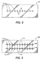
- the optical source of the printer 10 is a linear array 12 of vertical cavity surface emitting lasers (VCSELs) 14, as shown in Figure 3, all emitting nominally the same wavelength ⁇ 1 and same polarization state.
- VCSELs vertical cavity surface emitting lasers
- the individual VCSELs 14 in the array 12 shown in Figure 3 are arranged linearly in the scan plane direction with equal center to center spacing 16 between the individual VCSELs 14.
- the linear VCSEL array 12 is monolithic in the preferred embodiment.
- the monolithic VCSEL arrays can be made in many different ways.
- a high density array of vertical cavity surface emitting lasers can emit from the epitaxial side of the array, as described in US-A-5 062 115.
- a high density array of vertical cavity surface emitting lasers can also emit from the substrate side of the array, as described in US-A-5 216 263. In both cases, all elements of the array emit at substantially the same wavelength and have no provision for control of the polarization state.
- the VCSELs 14 in array 12 include polarization control such that each element emits in the same polarization state in order to eliminate pixel to pixel nonuniformity from polarization dependence in the transmission/reflection characteristics of optical filters and beam separators.
- the linear array 12 of vertical cavity surface emitting lasers (VCSELs) 14 will emit partially overlapping beams 18 of the same wavelength ⁇ 1 and the same polarization state.
- the VCSEL elements have a beam divergence of about 8 to 10 degrees at the 50% power points and are focused by an imaging lens system 20 onto surface 22 of the photoreceptor 24.
- each individual beam 18 from each individual VCSEL 14 in the linear array 12 is focused to a different individual pixel point 28 along a scan line 26 on the photoreceptor surface 22 in the scan plane.
- the beams 18 from the linear array 12 are focused by projection (imaging) lens 20 in both the scan and cross-scan plane to form a single scan line 26 on the photoreceptor surface 22. All the VCSELs in the linear array will be addressed at the same time so that the linear array will simultaneously expose the entire line on the photoreceptor 24.
- the imaging lens 20 receives the slightly diverging beams 18 from the array 12 and focuses the beams onto the photoreceptor surface 22.
- the imaging lens 20 also magnifies the beams 18 into the pixels 28 on the photoreceptor surface 22.
- the imaging lens can be a relatively inexpensive projection lens with an appropriate magnification and F/no.
- the optical magnification required for the imaging lens 22 is determined by the length of the array 12 because the full array must cover at least the width of a full sized page.
- monolithic structures are referred since the individual VCSELs in the array can be aligned during manufacture of the array, particularly photolithographic manufacture. Also, handling of the VCSEL array is minimized if one array is used rather than trying to bond linearly two or more separate subarrays together into one array.
- a convenient length for monolithic VCSEL arrays would be 35 mm since such arrays can be grown uniformly and handled without serious breakage within present III-V diode technology and 35mm projection lenses for the imaging lens 20 are readily available.
- an optical magnification of approximately 8.5 is needed to cover a scan width of 297mm (11.7in).
- the distance between the spots on the photoreceptor surface is 42 ⁇ m, which at 8.5X magnification requires a center-to-center spacing 16 in Figure 3 of 5 ⁇ m between individual VCSELs 14 in the array 12.
- the above optical geometry provides the proper magnification for the scan width and for the spot (pixel) separations along the scan line 26 on the photoreceptor 24.
- the spot size of each pixel 28 on the photoreceptor surface 22 shown in Figure 1 is determined by the F/no. of the imaging lens 20.
- the approximate F/no. required to resolve individual elements on 5 ⁇ m centers at 780nm is given by F/no. equal to 5 ⁇ m/1.0 ⁇ which equals 6.4.
- the lens 20 images the beam 18 of each laser element to a spot with a "full width half maximum" (FWHM) size of 42 ⁇ m, i.e. distance between spots for 600spi.
- FWHM full width half maximum
- adjacent spots on the photoreceptor surface 22 overlap at FWHM. Since individual lasers in a VCSEL array 12 have a half power beam divergence of about 8 to 10 degrees, an imaging lens 20 with an F/no.
- the highlight color printer 100 shown in Figure 4 utilizes a monolithic structure 102 of two linear arrays 108, 110 (as shown in Figure 5) of vertical cavity surface emitting lasers (VCSELs) 112, 116 to simultaneous expose two photoreceptors 130, 134 to enable one pass highlight color printing.
- VCSELs vertical cavity surface emitting lasers
- the monolithic array 102 of the printer 100 is selectively addressed by video image signals representing the image to be printed, processed through Electronic Sub System (ESS) 104 and controlled by drive circuit 106 to produce an intensity modulated beam from each individual VCSEL 112. 116 in the array 102.
- ESS Electronic Sub System
- the monolithic laser array structure 102 shown in Figure 5 consists of two linear VCSEL arrays 108 and 110 aligned parallel to each other within the monolithic array structure 102.
- the individual VCSELs 112 in the linear array 108 are arranged with equal center to center spacing 114 between the individual VCSELs 112.
- the individual VCSELs 116 in the linear array 110 are arranged with equal center to center spacing 114 between the individual VCSELs 116.
- Individual VCSELs 112 are aligned with individual VCSELs 116 in the direction orthogonal to the common linear direction of arrays 108 and 110.
- the monolithic array structure 102 is aligned so as to form two parallel scan lines orthogonal to the slow scan direction.
- the monolithic laser array structure 102 is symmetrically placed in both the slow scan and fast scan directions with respect to the optical axis of the imaging lens 122.
- symmetry is not required in principle, in practice it is highly recommended since a smaller object field for the projection lens permits simpler design and therefore lower cost.
- the VCSELs 112 in the linear array 108 emit light at a first wavelength.
- the VCSELs 116 in the linear array 110 emit light at a second wavelength.
- the wavelength of the beam is determined by the photoreceptor, 780nm is good for infrared sensitive photoreceptors while 680nm is good for red sensitive photoreceptors.
- the monolithic VCSEL array structure 102 with its two linear arrays 108 and 110 can be made in many different ways.
- a high density array of vertical cavity surface emitting lasers can emit from the epitaxial side of the array, as described in US-A-5 062 115.
- a high density array of vertical cavity surface emitting lasers can emit from the substrate side of the array, as described in US-A-5 216 263. In both cases, all elements of the array emit at substantially the same wavelength and have no provision for control of the polarization state.
- the array structure 102 may be either a monolithic diode laser array or two non-monolithic laser subarrays closely spaced into a single integrated array. With either type of source, the laser array structure 102 provides a substantially common spatial origin for both laser beams.
- the monolithic array structure 102 emits a linear array of modulated first wavelength beams 118 and a linear array of modulated second wavelength beams 120. Only the chief rays are shown for clarity.
- the beams 118 and 120 are slightly diverging from the array 102 and are focused and magnified by an imaging lens 122 as discussed previously.
- a wavelength beam separator 124 separates the laser beams 118 and 120 after they pass through the imaging lens 112.
- the wavelength beam separator 124 is a wavelength selective, multiple layer film, having the optical characteristics shown in Figure 6. Thus, for two wavelengths appropriately matched to the optical characteristics of the beam separator 124, e.g. 600nm and 650nm, a beam of one wavelength will be transmitted while a beam of the other wavelength will be reflected. Such beam separators are well known in the art. Reference may be made to Volume 1 of "Applied Optics and Optical Engineering", (1965) edited by R. Kingslake, for example at chapter 5, number IV and chapter 8, numbers VIII and IX.
- Mirrors 126 and 128 reflect the separated first wavelength laser beam 118 from the beam separator 124 onto a first photoreceptor 130, while mirror 132 reflects separated second wavelength laser beam 120 from the beam separator 124 onto a second photoreceptor 134.
- both beams 118 and 120 are from substantially the same spatial location and have substantially parallel optical axes, similarly dimensioned beams with equal optical path lengths are input to the beam separator 124.
- the problem of maintaining equal optical path length for each beam reduces to the much simpler problem of maintaining substantially equal optical path lengths from the beam separator 124 to the photoreceptors 130 and 134.
- Substantially equal optical path lengths are set by properly positioning mirrors 126, 128 and 132. Equalization of optical path lengths results in similarly dimensioned spots at each photoreceptor 130, 134.
- the imaging lens 122 forms a magnified image of each VCSEL array 108, 110 on the appropriate photoreceptor 130, 134.
- the path lengths from the imaging lens 122 to all photoreceptors 130, 134 are made equal so that the optical magnification of each linear array is the same in each arm of the system.
- a reasonable number for this distance is 533mm (21 in) which is compatible with the space allotted to one pass four colors/single polygon/single optics ROSs in current printer designs. Since adjacent linear arrays are imaged at different positions, the sagittal spacing between them can be as large as the field of view of the projection lens allows. This is because the output of each array is directed to its exposure position by the wavelength separators and mirrors as shown. Synchronization between exposures at different positions is controlled by the relative times at which the arrays are fired.
- the photoreceptors 130 and 134 are charged by a charging stations (not shown) prior to exposure by beams 118 and 120 respectively.
- a development station also not shown
- a fully developed image is then transferred to a single sheet (not shown) at a transfer station (not shown) from each of the two photoreceptors 130 and 134.
- the charge, development and transfer stations are conventional in the art. Further details of xerographic stations in a multiple exposure single pass system are disclosed in US-A-4 661 901; US-A-4 791 452; and US-A-4 833 503.
- the printer 100 may be used for two color printing where the image created on each photoreceptor 130 and 134 corresponds to a different system color. This color printing is typically black and a highlight color.
- the printer 100 shown in Figure 4 is a highlight color xerographic printer with a monolithic structure of two linear arrays 108, 110 of vertical cavity surface emitting lasers (VCSELs) 112, 116 to expose a position on two photoreceptors 130, 134.
- VCSELs vertical cavity surface emitting lasers
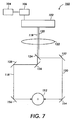
- the printer 150 shown in Figure 7 is a highlight color xerographic printer where the two linear arrays 108, 110 in the monolithic VCSEL array structure 102 expose two positions on a single photoreceptor 152 to enable one pass highlight color printing.
- the printer 150 shown in Figure 7 shows an alternate embodiment of printer 100 shown in Figure 4 wherein the light beams 118 and 120 are directed onto a single photoreceptor 152 by reflecting mirrors 154 and 156.
- Laser array structure 102 emits a first wavelength beam 118 and a second wavelength beam 120.
- the video signals for both beams are modulated by Electronic Sub System (ESS) 104 and drive circuit 106 as previously described.
- ESS Electronic Sub System
- the two beams 118 and 120 are focused and magnified by imaging lens 122 and separated by wavelength beam separator 124.
- Mirrors 126 and 128 reflect the separated first wavelength laser beam 118 from the beam separator 124, while mirror 132 reflects separated second wavelength laser beam 120 from the beam separator 124.
- the highlight color xerographic printer 150 of Figure 7 is the same as the highlight color xerographic printer 100 of Figure 4.
- the first wavelength laser beam 118 is reflected from mirror 128 and then reflected from mirror 156 onto one area of the photoreceptor 152.
- the second wavelength laser beam 120 is reflected from mirror 132 and then reflected from mirror 154 onto a separate area of the photoreceptor 152.
- the subsequent charge, development and transfer stations are conventional in the art.
- the wavelength beam separator 124 shown in Figures 4 and 7 transmits the first wavelength beam 118 while reflecting the second wavelength beam 120.
- An alternate means of separating beams of different wavelength is a pair of wavelength bandpass filters. However, a beam splitter is required and there is a resulting halving of the intensity of the beams upon the photoreceptors.
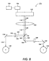
- the printer 175 shown in Figure 8 shows an alternate embodiment of printer 100 of Figure 4 wherein narrow bandpass filters 188, 190 are utilized to separate the light beams 118, 120 at different wavelengths.
- Laser array structure 102 of Figure 8 emits a first wavelength beam 118 and a second wavelength beam 120.
- the video signals for both beams are modulated by Electronic Sub System (ESS) 104 and drive circuit 106.
- ESS Electronic Sub System
- the two beams 118 and 120 are focused and magnified by imaging lens 122.
- the highlight color xerographic printer 150 of Figure 8 is the same as the highlight color xerographic printer 100 of Figure 4.
- the two beams 118 and 120 are then split by beam splitter 176.
- the first wavelength beam 118 is divided into beam 178 which is reflected from the beam splitter 176 and beam 180 which is transmitted through the beam splitter 176.
- the beams 178 and 180 have the same wavelength as the original first wavelength beam 118 but only half the intensity.
- the second wavelength beam 120 is divided into beam 182 which is reflected from the beam splitter 176 and beam 184 which is transmitted through the beam splitter 176.
- the beams 182 and 184 have the same wavelength as the original second wavelength beam 120 but only half the intensity.
- the beam splitter 176 is a partially transparent metallic film or multiple layer dielectric film constructed such that half the intensity of an incident beam is transmitted while the other half is reflected. Such beam splitters are well known to those skilled in the art and are frequently used optical components. Splitting both beams can be advantageous in spite of the increased power loss because it enables use of relatively low cost bandpass filters for beam separation.
- first wavelength light beam 180 and second wavelength light beam 184 are reflected by mirror 186 onto first narrow bandpass filter 188.
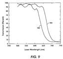
- the first narrow bandpass filter 188 has transmission characteristics as shown in Figure 9.
- the narrow bandpass filter is made from a material which blocks light beam of one wavelength while transmitting light of another wavelength.
- the filter 188 blocks first wavelength light beam 180 while transmitting second wavelength light beam 184.
- first wavelength light beam 178 and second wavelength light beam 182 are directed onto second narrow bandpass filter 190.
- Second narrow bandpass filter 190 has the opposite transmission characteristics as first filter 188. The filter 190 blocks second wavelength light beam 182 while transmitting first wavelength light beam 178.
- the first wavelength light beam 178 is reflected by mirror 128 onto the first photoreceptor 130 while the second wavelength light beam 184 is reflected by mirror 132 onto the second photoreceptor 134 in Figure 8.
- the distinction between the printer 100 of Figure 4 and the printer 175 of Figure 8 is that the wavelength beam separator 124 of Figure 4 is replaced with a beam splitter 176 and two narrow bandpass filters 188 and 190 of Figure 8 and that the beams 178, 184 on the photoreceptors 130, 134 in printer 175 of Figure 8 will have half the intensity of the comparable beams 118, 120 on the photoreceptors 130, 134 in printer 100 of Figure 4 for the same intensity emitted by elements in array 102.
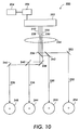
- a full color printer 200 is shown in Figure 10.
- the printer 200 utilizes a monolithic structure 202 ( Figure 11) of four linear arrays 208, 210, 212, 214 of vertical cavity surface emitting lasers (VCSELs) 216, 220, 222, 224 to expose four photoreceptors 244, 248, 250, 254 to enable one pass full color printing.
- VCSELs vertical cavity surface emitting lasers
- Each linear array 208, 210, 212, 214 emits at one of four different wavelengths.
- the monolithic array structure 202 of the printer 200 is selectively addressed by video image signals processed through Electronic Sub System (ESS) 204 and controlled by drive circuit 206 to produce a modulated beam from each individual VCSEL in the array.
- ESS Electronic Sub System
- the laser array structure 202 of Figure 11 consists of four linear VCSEL arrays 208, 210, 212 and 214 aligned and arranged in parallel with each other within the monolithic array 202. Individual VCSELs within each of the four linear arrays are arranged with equal center to center spacing 216 between individual VCSELs. Individual VCSELs in each linear array are aligned with individual VCSELs in the other linear arrays in the direction orthogonal to the common linear direction of the arrays. In the printer 200 ( Figure 10), the monolithic array structure 202 is aligned so as to form four parallel scan lines orthogonal to the slow scan direction. In the preferred embodiment, the monolithic laser array structure 202 is symmetrically placed with respect to the optical axis of the imaging lens 234 in both the slow scan and fast scan directions.
- the VCSELs 216 in the linear array 208 emit light at a first wavelength.
- the VCSELs 220 in the linear array 210 emit light at a second wavelength.
- the VCSELs 222 in the linear array 212 emit light at a third wavelength.
- the VCSELs 224 in the linear array 214 emit light in a fourth wavelength.
- the range of wavelengths is chosen to accommodate the responsivity of the photoreceptors 244, 248, 250, 254 and their proximity is limited by the selectivity of the optical filters.
- the VCSEL array structure 202 with its four linear arrays 208, 210, 212 and 214 may be either a monolithic diode laser array or two non-monolithic laser subarrays closely spaced into a single integrated array, as discussed previously.
- the monolithic array structure 202 emits a linear array of modulated first wavelength beams 226, modulated second wavelength beams 228, modulated third wavelength beams 230 and modulated fourth wavelength beams 232. Only the chief rays are shown for clarity.
- the beams 226, 228, 230 and 232 are diverging from the array 202 and are focused by an imaging lens 234 as discussed previously.
- the beam separator 236 is a wavelength selective multiple layer films having optical characteristics similar to those shown in Figure 6.
- the first wavelength beam separator 236 separates the first and second wavelength beams 226 and 230 from the third and fourth wavelength beams 228 and 232.
- the first and second wavelength beams 226 and 230 transmit through the first beam separator 236, reflect off mirror 238 and into the second wavelength beam separator 240 while third and fourth wavelength beams 228 and 232 reflect off the first beam separator 236 and into the third wavelength beam separator 242.
- the second and third wavelength beam separators 240 and 242 are wavelength selective multiple layer films having optical characteristics similar to those shown in Figure 12.
- the second beam separator 240 will reflect the beam 226 of the first wavelength onto a first photoreceptor 244.
- the beam separator 240 will transmit the beam 228 of the second wavelength which is reflected by mirror 246 onto the second photoreceptor 248.
- the third beam separator 242 will reflect the beam 228 of the third wavelength onto a third photoreceptor 250.
- the beam separator 242 will transmit the beam 232 of the fourth wavelength which is reflected by mirror 252 onto the fourth photoreceptor 254.
- each laser beam is independently modulated with image information, a distinct latent image is simultaneously printed on each photoreceptor 244, 248, 250, 254.
- the subsequent charge, development and transfer stations are conventional in the art.
- apparatus 200 may be used for full color reproduction, wherein the image on each photoreceptor 244, 248, 250, 254 corresponds to a different system color.
- the highlight color printer 100 of Figure 4 can be adapted with the addition of mirrors to expose two separated positions on a single photoreceptor rather than multiple photoreceptors.
- the full color printer 200 of Figure 10 can be adapted with the addition of mirrors to expose four separated positions on a single photoreceptor rather than multiple photoreceptors as illustrated.
- the full color printer 200 of Figure 10 can be adapted without additional mirrors to expose four separated positions on a single photoreceptive belt (not shown) rather than multiple photoreceptive drums as illustrated.
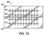
- the structure 300 is a non-monolithic combination of two monolithic structures 302 and 304 of VCSEL arrays, as mentioned previously.
- Each monolithic array structure 302, 304 contains two linear arrays of VCSELs emitting at different wavelengths.
- Monolithic array structure 302 has linear VCSEL array 306 emitting at a first wavelength and linear VCSEL array 308 emitting at a second wavelength.
- Monolithic array structure 304 has linear VCSEL array 310 emitting at a third wavelength and linear VCSEL array 312 emitting at the fourth wavelength.
- the laser array structure 300 of Figure 13 emits four different wavelengths, similar to the monolithic array structure 202 shown in Figure 11.
- the advantage of this non-monolithic combination is that each monolithic array structure 302 and 304 needs to emit only two wavelengths, thereby relaxing the requirements on the layer growths.
- the sagittal separation between adjacent arrays on different monolithic array structures can be much larger than the tangential spacing between the VCSEL elements, since each array is imaged at a different exposure position.
- the sagittal spacing between monolithic subarray structures is minimized by locating the linear arrays near the edge of each monolithic subarray structure.
- a non-monolithic combination of monolithic dual wavelength subarray structures is preferred to an all monolithic structure source because it minimizes the wavelength range over which the active layer must provide gain and grown laser mirrors must provide high reflectivity within each VCSEL in each monolithic structure.
- Gain guided VCSELs are well suited for the color printing applications of the embodiments because they exhibit essentially no astigmatism.
- variation of the imaging lens' focal length due to the wavelength dependence of its refractive index can be compensated by (1) adding a glass plate to one array or by (2) monolithically adding an appropriate diffractive lens to individual elements of one array, as described in US-A-5 073 041.
- a monolithic structure of two or four VCSEL arrays of the present invention is cheaper to manufacture than the two or four separate LED print bars of the prior art.
- the VCSEL arrays are accurately aligned within the monolithic structure as opposed to the prior art four separate LED print bars which must be accurately aligned with each other.
- a monolithic structure of two or four VCSEL arrays considerably reduces the size and total spatial volume of a color xerographic printer. Also monolithic source arrays are cost-effective since assemblies of multiple chips is reduced or in some cases eliminated.
- the imaging lens of the present invention can compensate for focal length dispersion either by color correcting the lens or by inserting a glass plate into the beams emitted by an array or by monolithically adding an appropriate diffractive lens to individual elements of an array.
- the complex and expensive optics of a prior art ROS system are reduced to the imaging lens of the present invention.
Landscapes
- Physics & Mathematics (AREA)
- Engineering & Computer Science (AREA)
- Optics & Photonics (AREA)
- General Engineering & Computer Science (AREA)
- Theoretical Computer Science (AREA)
- General Physics & Mathematics (AREA)
- General Health & Medical Sciences (AREA)
- Toxicology (AREA)
- Health & Medical Sciences (AREA)
- Multimedia (AREA)
- Signal Processing (AREA)
- Laser Beam Printer (AREA)
- Printers Or Recording Devices Using Electromagnetic And Radiation Means (AREA)
- Color Electrophotography (AREA)
Description
- This invention relates to a color xerographic printer and, more particularly, to a color xerographic printer with a monolithic structure of multiple linear arrays of surface emitting lasers with dissimilar wavelengths to simultaneously expose widely separated positions on the same or different photoreceptors.
- A Raster Output Scanner (ROS) or a Light Emitting Diode (LED) print bar, known as imagers, used in xerographic printers are well known in the art such as in EP-A-0 589 652 and US-A-5 402 436. The ROS or the LED print bar is positioned in an optical scan system to write an image on the surface of a moving photoreceptor belt.
- In a ROS system, a modulated beam is directed onto the facets of a rotating polygon mirror which then sweeps the reflected beam across the photoreceptor surface. Each sweep exposes a raster line to a linear segment of a video signal image.
- However, the use of a rotating polygon mirror presents several inherent problems. Bow and wobble of the beam scanning across the photoreceptor surface result from imperfections in the mirror or even slight misangling of the mirror or from the instability of the rotation of the polygon mirror. These problems typically require complex, precise and expensive optical elements between the light source and the rotating polygon mirror and between the rotating polygon mirror and the photoreceptor surface. Additionally, optically complex elements are also needed to compensate for refractive index dispersion that causes changes in the focal length of the imaging optics of the ROS.
- The LED print bar generally consists of a linear array of light emitting diodes. Each LED in the linear array is used to expose a corresponding area on a moving photoreceptor in response to the video data information applied to the drive circuits of the print bars. The photoreceptor is advanced in the process direction to provide a desired image by the formation of sequential scan lines.
- In a color xerographic printer, a plurality of the light emitting elements of the LED print bars are imaged to a photoreceptor surface usually by closely spaced radially indexed glass fibers known as "selfoc" lenses.
- Printing with LED bars requires a precisely fabricated "selfoc" lens for each light emitting element. Each "selfoc" lens array must be straight and parallel with highly polished input and output facets. Each lens within the array must have the same focal length and throughput efficiency. Even if these requirements are met, the "selfoc" lenses have short focal lengths and therefore must be positioned close to the photoreceptor surface where the lenses can collect toner and thereby require an additional cleaning mechanism. Due to their optical characteristics, the depth of focus of a "selfoc" lens is very short and consequently requires very precise placement to produce uniform spot exposures on the scan line.
- Light emitting diodes, by their very nature, have a large angular divergence, a broad spectrum and are unpolarized, all factors which severely limit their use in color printing systems using a wavelength or polarization based scan line separation technique. Prior LED print bar xerographic line printers have taught only line exposure at a single position on one photoreceptor.
- US-A-5 337 074 and US-A-5 461 413 disclose using a single linear surface emitting laser array as the light source for a line printer.
- A laser array such as known from "High-Speed and High-Resolution Laser Printer", IBM Technical Disclosure Bulletin XXXIII (2), 1990, 307-310 has a smaller angular beam divergence than an LED array and therefore provides a higher power throughput efficiency. A laser array also has a smaller radiating aperture (source size) than an LED array and therefore can provide increased spot density. The narrow spectrum of laser beams enables optical separation of the laser beams as taught in the present application. The broad spectrum precludes similar separations of LED emissions.
- It is an object of this invention to provide a color xerographic line printer with simple and inexpensive optics and a single light source.
- It is yet another object of this invention to provide a color xerographic line printer with a multiple laser array light source with dissimilar wavelengths.
- In accordance with one aspect of the present invention as defined in the claims below, there is provided a color xerographic line printer comprising:- at least one photoreceptor, at least two linear laser arrays for emitting at least two modulated light beams of differing wavelengths, imaging lens means for imaging each modulated light beam onto at least one of the photoreceptor, and wavelength separation means for separating each modulated light beam onto a specific region of said at least one photoreceptor to simultaneously expose a full scan line thereon.
- In the present invention, a color printer uses multiple linear arrays of surface emitting lasers of differing wavelengths to simultaneously expose widely separated positions on the same or different photoreceptors. A highlight color printer would use two linear laser arrays while a full color printer would use four linear laser arrays.
- Each array is imaged to the photoreceptor by the same optical system. The multiple linear arrays can be closely spaced in a monolithic structure or assembled in a precise unit. Light emitting elements in each array can be spaced or staggered for line imaging at the printed pixel density.
- Other objects and attainments together with a fuller understanding of the invention will become apparent and appreciated by referring to the following description, by way of example only, taken in conjunction with the accompanying drawings in which:-
- Figure 1 is a schematic illustration of the cross-section scan plane view of a xerographic printer with a monolithic linear array of vertical cavity surface emitting lasers (VCSELs) which are described in L. Ogara et al, "A Multiple Wavelength Vertical-Cavity Surface-Emitting Laser (VCSEL) Array for Optical Interconnection", IEICE Transactions on Electronics E78-C (1), 1995, 22-27.
- Figure 2 is a schematic illustration of the cross-section cross-scan plane view of the xerographic printer with a monolithic linear array of vertical cavity surface emitting lasers (VCSELs) shown in Figure 1;
- Figure 3 is a schematic illustration of the cross-section side view of the monolithic linear array of vertical cavity surface emitting lasers (VCSELs) of the xerographic printer shown in Figures 1 and 2;
- Figure 4 is a schematic illustration of the cross-section side view of a highlight color xerographic printer with monolithic multiple linear arrays of vertical cavity surface emitting lasers (VCSELs) and two photoreceptors formed according to the present invention;
- Figure 5 is a schematic illustration of the cross-section side view of the monolithic multiple linear arrays of vertical cavity surface emitting lasers (VCSELs) shown in Figure 4 formed according to the present invention;
- Figure 6 shows the reflection/transmission characteristics of a wavelength beam separator (as used in various embodiments of the present invention);
- Figure 7 is a schematic illustration of the cross-section side view of an alternate embodiment of a highlight color xerographic printer with monolithic multiple linear arrays of vertical cavity surface emitting lasers (VCSELs) and a single photoreceptor formed according to the present invention;
- Figure 8 is a schematic illustration of the cross-section side view of an alternate embodiment of the highlight color xerographic printer with monolithic multiple linear arrays of vertical cavity surface emitting lasers (VCSELs) and beam separators and two photoreceptors formed according to the present invention;
- Figure 9 shows the absorption/transmission characteristics of a narrow bandpass filter as used in the highlight color xerographic printer shown in Figure 8;
- Figure 10 is a schematic illustration of the cross-section side view of a full color xerographic printer with monolithic multiple linear arrays of vertical cavity surface emitting lasers (VCSELs) and four photoreceptors formed according to the present invention;
- Figure 11 is a schematic illustration of the cross-section side view of the monolithic multiple linear arrays of vertical cavity surface emitting lasers (VCSELs) shown in Figure 10 formed according to the present invention;
- Figure 12 shows the reflection/transmission characteristics of a wavelength beam separator of the full color xerographic printer shown in Figure 10; and
- Figure 13 is a schematic illustration of the cross-section side view of the nonmonolithic structure combination of two monolithic multiple linear arrays of vertical cavity surface emitting lasers (VCSELs) formed according to the present invention.
-
- Reference is now made to Figures 1 and 2 wherein is described the basic
xerographic printer 10 as used in the illustrated embodiments of the present invention. Figures 1 and 2 show the line projection architecture of theprinter 10. The optical source of theprinter 10 is alinear array 12 of vertical cavity surface emitting lasers (VCSELs) 14, as shown in Figure 3, all emitting nominally the same wavelength λ1 and same polarization state. - The
individual VCSELs 14 in thearray 12 shown in Figure 3 are arranged linearly in the scan plane direction with equal center tocenter spacing 16 between theindividual VCSELs 14. Thelinear VCSEL array 12 is monolithic in the preferred embodiment. - The monolithic VCSEL arrays can be made in many different ways. A high density array of vertical cavity surface emitting lasers can emit from the epitaxial side of the array, as described in US-A-5 062 115. A high density array of vertical cavity surface emitting lasers can also emit from the substrate side of the array, as described in US-A-5 216 263. In both cases, all elements of the array emit at substantially the same wavelength and have no provision for control of the polarization state. For embodiments of the present invention, the VCSELs 14 in
array 12 include polarization control such that each element emits in the same polarization state in order to eliminate pixel to pixel nonuniformity from polarization dependence in the transmission/reflection characteristics of optical filters and beam separators. - Returning to the line projection architecture of the the basic
xerographic printer 10 shown in Figures 1 and 2, thelinear array 12 of vertical cavity surface emitting lasers (VCSELs) 14 will emit partially overlappingbeams 18 of the same wavelength λ1 and the same polarization state. The VCSEL elements have a beam divergence of about 8 to 10 degrees at the 50% power points and are focused by animaging lens system 20 ontosurface 22 of thephotoreceptor 24. - As shown in Figure 1, each
individual beam 18 from each individual VCSEL 14 in thelinear array 12 is focused to a differentindividual pixel point 28 along ascan line 26 on thephotoreceptor surface 22 in the scan plane. As shown in Figure 2, thebeams 18 from thelinear array 12 are focused by projection (imaging)lens 20 in both the scan and cross-scan plane to form asingle scan line 26 on thephotoreceptor surface 22. All the VCSELs in the linear array will be addressed at the same time so that the linear array will simultaneously expose the entire line on thephotoreceptor 24. - The
imaging lens 20 receives the slightlydiverging beams 18 from thearray 12 and focuses the beams onto thephotoreceptor surface 22. Theimaging lens 20 also magnifies thebeams 18 into thepixels 28 on thephotoreceptor surface 22. Typically, the imaging lens can be a relatively inexpensive projection lens with an appropriate magnification and F/no. - The optical magnification required for the
imaging lens 22 is determined by the length of thearray 12 because the full array must cover at least the width of a full sized page. Although it is possible to stitch separate subarrays together linearly to make a long array, monolithic structures are referred since the individual VCSELs in the array can be aligned during manufacture of the array, particularly photolithographic manufacture. Also, handling of the VCSEL array is minimized if one array is used rather than trying to bond linearly two or more separate subarrays together into one array. - A convenient length for monolithic VCSEL arrays would be 35 mm since such arrays can be grown uniformly and handled without serious breakage within present III-V diode technology and 35mm projection lenses for the
imaging lens 20 are readily available. - In an illustrative embodiment of Figure 1 with a 35mm
long VCSEL array 12 and a 35mm format projection/imaging lens 20, an optical magnification of approximately 8.5 is needed to cover a scan width of 297mm (11.7in). For an exposure density of 600spi (spots per inch) along thescan line 26 on thephotoreceptor surface 22 in the scan plane, the distance between the spots on the photoreceptor surface is 42µm, which at 8.5X magnification requires a center-to-center spacing 16 in Figure 3 of 5µm betweenindividual VCSELs 14 in thearray 12. The above optical geometry provides the proper magnification for the scan width and for the spot (pixel) separations along thescan line 26 on thephotoreceptor 24. - The spot size of each
pixel 28 on thephotoreceptor surface 22 shown in Figure 1 is determined by the F/no. of theimaging lens 20. The approximate F/no. required to resolve individual elements on 5µm centers at 780nm is given by F/no. equal to 5µm/1.0λ which equals 6.4. With this F/no., thelens 20 images thebeam 18 of each laser element to a spot with a "full width half maximum" (FWHM) size of 42µm, i.e. distance between spots for 600spi. Thus, adjacent spots on thephotoreceptor surface 22 overlap at FWHM. Since individual lasers in aVCSEL array 12 have a half power beam divergence of about 8 to 10 degrees, animaging lens 20 with an F/no. which equals 6.4 will collect essentially all of the light emitted by eachVCSEL element 14 at FWHM. If the light is to be collected at 1/e2, the working F/no. of thelens 20 should be around 3.6. Therefore, the optical efficiency of thisprinting system 10 can be very high. - The
highlight color printer 100 shown in Figure 4 utilizes amonolithic structure 102 of twolinear arrays 108, 110 (as shown in Figure 5) of vertical cavity surface emitting lasers (VCSELs) 112, 116 to simultaneous expose twophotoreceptors - The
monolithic array 102 of theprinter 100 is selectively addressed by video image signals representing the image to be printed, processed through Electronic Sub System (ESS) 104 and controlled bydrive circuit 106 to produce an intensity modulated beam from eachindividual VCSEL 112. 116 in thearray 102. - The monolithic
laser array structure 102 shown in Figure 5 consists of twolinear VCSEL arrays monolithic array structure 102. Theindividual VCSELs 112 in thelinear array 108 are arranged with equal center to center spacing 114 between theindividual VCSELs 112. Theindividual VCSELs 116 in thelinear array 110 are arranged with equal center to center spacing 114 between theindividual VCSELs 116.Individual VCSELs 112 are aligned withindividual VCSELs 116 in the direction orthogonal to the common linear direction ofarrays printer 100 shown in Figure 4, themonolithic array structure 102 is aligned so as to form two parallel scan lines orthogonal to the slow scan direction. In the preferred embodiment, the monolithiclaser array structure 102 is symmetrically placed in both the slow scan and fast scan directions with respect to the optical axis of theimaging lens 122. Although symmetry is not required in principle, in practice it is highly recommended since a smaller object field for the projection lens permits simpler design and therefore lower cost. - The
VCSELs 112 in thelinear array 108 emit light at a first wavelength. TheVCSELs 116 in thelinear array 110 emit light at a second wavelength. The wavelength of the beam is determined by the photoreceptor, 780nm is good for infrared sensitive photoreceptors while 680nm is good for red sensitive photoreceptors. - The monolithic
VCSEL array structure 102 with its twolinear arrays A-5 216 263. In both cases, all elements of the array emit at substantially the same wavelength and have no provision for control of the polarization state. - The
array structure 102 may be either a monolithic diode laser array or two non-monolithic laser subarrays closely spaced into a single integrated array. With either type of source, thelaser array structure 102 provides a substantially common spatial origin for both laser beams. - Returning to the
highlight color printer 100 shown in Figure 4, themonolithic array structure 102 emits a linear array of modulated first wavelength beams 118 and a linear array of modulated second wavelength beams 120. Only the chief rays are shown for clarity. - The
beams array 102 and are focused and magnified by animaging lens 122 as discussed previously. Awavelength beam separator 124 separates thelaser beams imaging lens 112. - The
wavelength beam separator 124 is a wavelength selective, multiple layer film, having the optical characteristics shown in Figure 6. Thus, for two wavelengths appropriately matched to the optical characteristics of thebeam separator 124, e.g. 600nm and 650nm, a beam of one wavelength will be transmitted while a beam of the other wavelength will be reflected. Such beam separators are well known in the art. Reference may be made toVolume 1 of "Applied Optics and Optical Engineering", (1965) edited by R. Kingslake, for example at chapter 5, number IV andchapter 8, numbers VIII and IX. -
Mirrors wavelength laser beam 118 from thebeam separator 124 onto afirst photoreceptor 130, whilemirror 132 reflects separated secondwavelength laser beam 120 from thebeam separator 124 onto asecond photoreceptor 134. - Since both
beams beam separator 124. Thus, the problem of maintaining equal optical path length for each beam reduces to the much simpler problem of maintaining substantially equal optical path lengths from thebeam separator 124 to thephotoreceptors mirrors photoreceptor - The
imaging lens 122 forms a magnified image of eachVCSEL array appropriate photoreceptor imaging lens 122 to allphotoreceptors - The
photoreceptors beams photoreceptors - The
printer 100 may be used for two color printing where the image created on eachphotoreceptor - The
printer 100 shown in Figure 4 is a highlight color xerographic printer with a monolithic structure of twolinear arrays photoreceptors - The
printer 150 shown in Figure 7 is a highlight color xerographic printer where the twolinear arrays VCSEL array structure 102 expose two positions on asingle photoreceptor 152 to enable one pass highlight color printing. - The
printer 150 shown in Figure 7 shows an alternate embodiment ofprinter 100 shown in Figure 4 wherein the light beams 118 and 120 are directed onto asingle photoreceptor 152 by reflectingmirrors Laser array structure 102 emits afirst wavelength beam 118 and asecond wavelength beam 120. The video signals for both beams are modulated by Electronic Sub System (ESS) 104 and drivecircuit 106 as previously described. The twobeams lens 122 and separated bywavelength beam separator 124.Mirrors wavelength laser beam 118 from thebeam separator 124, whilemirror 132 reflects separated secondwavelength laser beam 120 from thebeam separator 124. Thus far, the highlightcolor xerographic printer 150 of Figure 7 is the same as the highlightcolor xerographic printer 100 of Figure 4. - However in the highlight
color xerographic printer 150 of Figure 7, the firstwavelength laser beam 118 is reflected frommirror 128 and then reflected frommirror 156 onto one area of thephotoreceptor 152. The secondwavelength laser beam 120 is reflected frommirror 132 and then reflected frommirror 154 onto a separate area of thephotoreceptor 152. As noted previously, the subsequent charge, development and transfer stations are conventional in the art. - The
wavelength beam separator 124 shown in Figures 4 and 7 transmits thefirst wavelength beam 118 while reflecting thesecond wavelength beam 120. An alternate means of separating beams of different wavelength is a pair of wavelength bandpass filters. However, a beam splitter is required and there is a resulting halving of the intensity of the beams upon the photoreceptors. - The
printer 175 shown in Figure 8 shows an alternate embodiment ofprinter 100 of Figure 4 wherein narrowbandpass filters light beams Laser array structure 102 of Figure 8 emits afirst wavelength beam 118 and asecond wavelength beam 120. The video signals for both beams are modulated by Electronic Sub System (ESS) 104 and drivecircuit 106. The twobeams lens 122. Thus far, the highlightcolor xerographic printer 150 of Figure 8 is the same as the highlightcolor xerographic printer 100 of Figure 4. - The two
beams beam splitter 176. Thefirst wavelength beam 118 is divided intobeam 178 which is reflected from thebeam splitter 176 andbeam 180 which is transmitted through thebeam splitter 176. Thebeams first wavelength beam 118 but only half the intensity. Similarly, thesecond wavelength beam 120 is divided intobeam 182 which is reflected from thebeam splitter 176 andbeam 184 which is transmitted through thebeam splitter 176. Thebeams second wavelength beam 120 but only half the intensity. - The
beam splitter 176 is a partially transparent metallic film or multiple layer dielectric film constructed such that half the intensity of an incident beam is transmitted while the other half is reflected. Such beam splitters are well known to those skilled in the art and are frequently used optical components. Splitting both beams can be advantageous in spite of the increased power loss because it enables use of relatively low cost bandpass filters for beam separation. - After transmission through the
beam splitter 176, firstwavelength light beam 180 and secondwavelength light beam 184 are reflected bymirror 186 onto firstnarrow bandpass filter 188. The firstnarrow bandpass filter 188 has transmission characteristics as shown in Figure 9. The narrow bandpass filter is made from a material which blocks light beam of one wavelength while transmitting light of another wavelength. Thefilter 188 blocks firstwavelength light beam 180 while transmitting secondwavelength light beam 184. - Similarly, after reflection from the
beam splitter 176, firstwavelength light beam 178 and secondwavelength light beam 182 are directed onto secondnarrow bandpass filter 190. Secondnarrow bandpass filter 190 has the opposite transmission characteristics asfirst filter 188. Thefilter 190 blocks secondwavelength light beam 182 while transmitting firstwavelength light beam 178. - Then returning to the same optical path and optical components as the
printer 100 of Figure 4, the firstwavelength light beam 178 is reflected bymirror 128 onto thefirst photoreceptor 130 while the secondwavelength light beam 184 is reflected bymirror 132 onto thesecond photoreceptor 134 in Figure 8. - Outside of mirrors to reflect the beams and adjust the optical path length, the distinction between the
printer 100 of Figure 4 and theprinter 175 of Figure 8 is that thewavelength beam separator 124 of Figure 4 is replaced with abeam splitter 176 and twonarrow bandpass filters beams photoreceptors printer 175 of Figure 8 will have half the intensity of thecomparable beams photoreceptors printer 100 of Figure 4 for the same intensity emitted by elements inarray 102. - A
full color printer 200 is shown in Figure 10. Theprinter 200 utilizes a monolithic structure 202 (Figure 11) of fourlinear arrays photoreceptors linear array - The
monolithic array structure 202 of theprinter 200 is selectively addressed by video image signals processed through Electronic Sub System (ESS) 204 and controlled bydrive circuit 206 to produce a modulated beam from each individual VCSEL in the array. - The
laser array structure 202 of Figure 11 consists of fourlinear VCSEL arrays monolithic array 202. Individual VCSELs within each of the four linear arrays are arranged with equal center to center spacing 216 between individual VCSELs. Individual VCSELs in each linear array are aligned with individual VCSELs in the other linear arrays in the direction orthogonal to the common linear direction of the arrays. In the printer 200 (Figure 10), themonolithic array structure 202 is aligned so as to form four parallel scan lines orthogonal to the slow scan direction. In the preferred embodiment, the monolithiclaser array structure 202 is symmetrically placed with respect to the optical axis of theimaging lens 234 in both the slow scan and fast scan directions. - The
VCSELs 216 in thelinear array 208 emit light at a first wavelength. TheVCSELs 220 in thelinear array 210 emit light at a second wavelength. TheVCSELs 222 in thelinear array 212 emit light at a third wavelength. TheVCSELs 224 in thelinear array 214 emit light in a fourth wavelength. The range of wavelengths is chosen to accommodate the responsivity of thephotoreceptors - The
VCSEL array structure 202 with its fourlinear arrays - The
monolithic array structure 202 emits a linear array of modulated first wavelength beams 226, modulated second wavelength beams 228, modulated third wavelength beams 230 and modulated fourth wavelength beams 232. Only the chief rays are shown for clarity. - The
beams array 202 and are focused by animaging lens 234 as discussed previously. A firstwavelength beam separator 236, separates thelaser beams imaging lens 234. Thebeam separator 236 is a wavelength selective multiple layer films having optical characteristics similar to those shown in Figure 6. - The first
wavelength beam separator 236 separates the first and second wavelength beams 226 and 230 from the third and fourth wavelength beams 228 and 232. The first and second wavelength beams 226 and 230 transmit through thefirst beam separator 236, reflect offmirror 238 and into the secondwavelength beam separator 240 while third and fourth wavelength beams 228 and 232 reflect off thefirst beam separator 236 and into the thirdwavelength beam separator 242. - The second and third
wavelength beam separators - Thus, the
second beam separator 240 will reflect thebeam 226 of the first wavelength onto afirst photoreceptor 244. Thebeam separator 240 will transmit thebeam 228 of the second wavelength which is reflected by mirror 246 onto thesecond photoreceptor 248. - The
third beam separator 242 will reflect thebeam 228 of the third wavelength onto athird photoreceptor 250. Thebeam separator 242 will transmit thebeam 232 of the fourth wavelength which is reflected bymirror 252 onto thefourth photoreceptor 254. - Since each laser beam is independently modulated with image information, a distinct latent image is simultaneously printed on each
photoreceptor apparatus 200 may be used for full color reproduction, wherein the image on eachphotoreceptor - Since all of the
beams wavelength beam separator 236. Thus the problem of maintaining equal optical path lengths for each beam reduces to the much simpler problem of maintaining substantially equal optical path lengths from the firstwavelength beam separator 236 to the individual photoreceptors. Substantially equal optical path lengths are set by adjusting the individual optical path lengths by properly positioningmirrors - As shown in the
highlight color printer 150 of Figure 7, thehighlight color printer 100 of Figure 4 can be adapted with the addition of mirrors to expose two separated positions on a single photoreceptor rather than multiple photoreceptors. Similarly, thefull color printer 200 of Figure 10 can be adapted with the addition of mirrors to expose four separated positions on a single photoreceptor rather than multiple photoreceptors as illustrated. Alternatively, thefull color printer 200 of Figure 10 can be adapted without additional mirrors to expose four separated positions on a single photoreceptive belt (not shown) rather than multiple photoreceptive drums as illustrated. - Sets comprising a beam splitter and two wavelength bandpass filters for wavelength separation could be utilized in the color xerographic line printer for the initial wavelength separation and the two subsequent wavelength separations. However, the resulting intensity of each beam upon the photoreceptor is now a quarter of its intensity from the multiple laser array light source.
- Another
laser array structure 300 is shown in Figure 13. Thestructure 300 is a non-monolithic combination of twomonolithic structures monolithic array structure Monolithic array structure 302 haslinear VCSEL array 306 emitting at a first wavelength andlinear VCSEL array 308 emitting at a second wavelength.Monolithic array structure 304 haslinear VCSEL array 310 emitting at a third wavelength andlinear VCSEL array 312 emitting at the fourth wavelength. - Thus, the
laser array structure 300 of Figure 13 emits four different wavelengths, similar to themonolithic array structure 202 shown in Figure 11. The advantage of this non-monolithic combination is that eachmonolithic array structure - The sagittal separation between adjacent arrays on different monolithic array structures can be much larger than the tangential spacing between the VCSEL elements, since each array is imaged at a different exposure position. The sagittal spacing between monolithic subarray structures is minimized by locating the linear arrays near the edge of each monolithic subarray structure. However it is important to have array elements on different monolithic subarray structures aligned sagitally in order to avoid scan line alignment on the four development stations. Precise alignment of the scan lines at different stations is required since the four images are transferred serially to paper or an intermediate transfer belt. A non-monolithic combination of monolithic dual wavelength subarray structures is preferred to an all monolithic structure source because it minimizes the wavelength range over which the active layer must provide gain and grown laser mirrors must provide high reflectivity within each VCSEL in each monolithic structure.
- Gain guided VCSELs are well suited for the color printing applications of the embodiments because they exhibit essentially no astigmatism. In addition, variation of the imaging lens' focal length due to the wavelength dependence of its refractive index can be compensated by (1) adding a glass plate to one array or by (2) monolithically adding an appropriate diffractive lens to individual elements of one array, as described in US-A-5 073 041.
- A monolithic structure of two or four VCSEL arrays of the present invention is cheaper to manufacture than the two or four separate LED print bars of the prior art. The VCSEL arrays are accurately aligned within the monolithic structure as opposed to the prior art four separate LED print bars which must be accurately aligned with each other.
- A monolithic structure of two or four VCSEL arrays considerably reduces the size and total spatial volume of a color xerographic printer. Also monolithic source arrays are cost-effective since assemblies of multiple chips is reduced or in some cases eliminated.
- The imaging lens of the present invention can compensate for focal length dispersion either by color correcting the lens or by inserting a glass plate into the beams emitted by an array or by monolithically adding an appropriate diffractive lens to individual elements of an array. The complex and expensive optics of a prior art ROS system are reduced to the imaging lens of the present invention.
Claims (11)
- A color xerographic line printer (100; 150; 175; 200) comprising:-at least one photoreceptor (130, 134; 152; 244, 248, 250, 254),at least two linear laser arrays (108, 110; 208, 210, 212, 214) for emitting at least two modulated light beams (118, 120; 226, 228, 232, 232) of differing wavelengths,imaging lens means (122; 234) for imaging each modulated light beam (118, 120; 226, 228, 230, 232) onto at least one of the photoreceptor (130, 134; 152; 244, 248, 250, 254), andwavelength separation means (124; 176, 188, 190; 236, 242, 242) for separating each modulated light beam (118, 120; 226, 228, 232, 232) onto a specific region of said at least one photoreceptor (130, 134; 152; 244, 248, 250, 254) to simultaneously expose a full scan line thereon.
- A printer according to claim 1 comprising at least two photoreceptors (130, 134; 244, 248, 250, 254), the wavelength separation means (124; 236, 240, 242) separating each modulated light beam (118, 120; 226, 228, 230, 232) onto respective different regions on respective photoreceptors (130, 134; 244, 248, 250, 254).
- A printer (150) according to to claim 1 for printing highlight color comprising a single photoreceptor (152) and first and second linear laser arrays (108, 110), the wavelength separation means (124) separating the first and second modulated light beams (118, 120) onto respective first and second regions of the photoreceptor (152).
- A printer (100) according to claim 1 for printing a highlight color comprising first and second photoreceptors (130, 134) and first and second linear laser arrays (108, 110), the wavelength separation means (124) separating the first and second modulated light beams (118, 120) onto respective first and second photoreceptors (130, 134).
- A printer according to claim 1 for printing full color comprising a single photoreceptor, first, second, third and fourth linear laser arrays (208, 210, 212, 214) for emitting respective first, second, third and fourth modulated light beams (226, 228, 230, 232), the wavelength separation means (236, 240, 242) for separating the first, second, third and fourth modulated light beams (226, 228, 230, 232) onto respective first, second, third and fourth regions of the photoreceptor.
- A printer (200) according to claim 1 for printing full color comprising first, second, third and fourth photoreceptors (244, 248, 250, 254) and first, second, third and fourth linear laser arrays (208, 210, 212, 214), the wavelength separation means (236, 240, 242) separating the first, second, third and fourth modulated light beams (226, 228, 230, 232) onto respective ones of the first, second, third and fourth photoreceptors (244, 248, 250, 254).
- A printer according to any one of the preceding claims wherein the wavelength separation means is a multiple layer film beam separator (124; 236, 240, 242).
- A printer according to any one of claims 1 to 6 wherein the wavelength separation means is a beam splitter (176) and two bandpass filters (188, 190).
- A printer according to claim 5 or 6 wherein the wavelength separation means is three sets of multiple layer film beam separators (236, 240, 244).
- A printer according to claim 5 or 6 wherein the wavelength separation means is three sets of a beam splitter (176) and two bandpass filters (188, 190).
- A printer according to claim 5 or 6 wherein the wavelength separation means is at least one set of a multiple layer film beam separator (124) and at least one set of a beam splitter (176) and two bandpass filters (188, 190).
Applications Claiming Priority (2)
| Application Number | Priority Date | Filing Date | Title |
|---|---|---|---|
| US57779495A | 1995-12-22 | 1995-12-22 | |
| US577794 | 1995-12-22 |
Publications (2)
| Publication Number | Publication Date |
|---|---|
| EP0781663A1 EP0781663A1 (en) | 1997-07-02 |
| EP0781663B1 true EP0781663B1 (en) | 2000-07-19 |
Family
ID=24310197
Family Applications (1)
| Application Number | Title | Priority Date | Filing Date |
|---|---|---|---|
| EP19960308991 Expired - Lifetime EP0781663B1 (en) | 1995-12-22 | 1996-12-11 | Color xerographic printer with multiple linear arrays of surface emitting lasers with dissimilar wavelengths |
Country Status (3)
| Country | Link |
|---|---|
| EP (1) | EP0781663B1 (en) |
| JP (1) | JPH09183253A (en) |
| DE (1) | DE69609400T2 (en) |
Family Cites Families (3)
| Publication number | Priority date | Publication date | Assignee | Title |
|---|---|---|---|---|
| US5461413A (en) * | 1991-07-22 | 1995-10-24 | At&T Ipm Corp. | Laser array printing |
| US5341158A (en) * | 1992-09-22 | 1994-08-23 | Xerox Corporation | Raster output scanner for a xerographic printing system having laser diodes arranged in a line parallel to the fast scan direction |
| US5402436A (en) * | 1993-12-29 | 1995-03-28 | Xerox Corporation | Nonmonolithic array structure of multiple beam diode lasers |
-
1996
- 1996-12-11 EP EP19960308991 patent/EP0781663B1/en not_active Expired - Lifetime
- 1996-12-11 DE DE1996609400 patent/DE69609400T2/en not_active Expired - Fee Related
- 1996-12-13 JP JP33393596A patent/JPH09183253A/en not_active Withdrawn
Also Published As
| Publication number | Publication date |
|---|---|
| EP0781663A1 (en) | 1997-07-02 |
| DE69609400D1 (en) | 2000-08-24 |
| JPH09183253A (en) | 1997-07-15 |
| DE69609400T2 (en) | 2000-12-07 |
Similar Documents
| Publication | Publication Date | Title |
|---|---|---|
| EP0781662B1 (en) | Color xerographic printer with multiple linear arrays of surface emitting lasers with dissimilar polarization states and dissimilar wavelengths | |
| US5325381A (en) | Multiple beam diode laser output scanning system | |
| US6239828B1 (en) | Image formation device for forming a color image composed of plural colors | |
| US5341158A (en) | Raster output scanner for a xerographic printing system having laser diodes arranged in a line parallel to the fast scan direction | |
| US5371526A (en) | Raster output scanner for a single pass printing system which separates plural laser beams by wavelength and polarization | |
| US5691761A (en) | Method and apparatus for multi-channel printing in a raster output scanning system | |
| EP0710009B1 (en) | Method and apparatus reducing differences in images heights of images generated by plural light beams having dissimilar wavelengths | |
| US5574491A (en) | Apparatus spot position control in an output device employing a linear array of light sources | |
| US5343224A (en) | Diode laser multiple output scanning system | |
| JP2001133707A (en) | Scanning optical device | |
| US5485194A (en) | Optical scanning apparatus | |
| JP2004163740A (en) | Multi-beam scanning optical device and image forming apparatus using the same | |
| EP0781663B1 (en) | Color xerographic printer with multiple linear arrays of surface emitting lasers with dissimilar wavelengths | |
| US7151624B2 (en) | Light scanning unit | |
| EP0782928B1 (en) | Color xerographic printer with multiple linear arrays of surface emitting lasers with the same wavelengths | |
| JPH06106775A (en) | Laser recorder | |
| US5854705A (en) | Micropositioned laser source for raster output scanners | |
| JP2863664B2 (en) | Image recording device | |
| EP0747777B1 (en) | Colour printer with a single pass of the photoreceptor | |
| US7202986B2 (en) | Light scanning unit | |
| JP2005250103A (en) | Multi-beam scanning optical apparatus and image forming apparatus using the same | |
| JP2003177345A (en) | Light beam scanning device and image forming device |
Legal Events
| Date | Code | Title | Description |
|---|---|---|---|
| PUAI | Public reference made under article 153(3) epc to a published international application that has entered the european phase |
Free format text: ORIGINAL CODE: 0009012 |
|
| AK | Designated contracting states |
Kind code of ref document: A1 Designated state(s): DE FR GB |
|
| 17P | Request for examination filed |
Effective date: 19980102 |
|
| GRAG | Despatch of communication of intention to grant |
Free format text: ORIGINAL CODE: EPIDOS AGRA |
|
| 17Q | First examination report despatched |
Effective date: 19990921 |
|
| GRAG | Despatch of communication of intention to grant |
Free format text: ORIGINAL CODE: EPIDOS AGRA |
|
| GRAH | Despatch of communication of intention to grant a patent |
Free format text: ORIGINAL CODE: EPIDOS IGRA |
|
| GRAH | Despatch of communication of intention to grant a patent |
Free format text: ORIGINAL CODE: EPIDOS IGRA |
|
| GRAA | (expected) grant |
Free format text: ORIGINAL CODE: 0009210 |
|
| AK | Designated contracting states |
Kind code of ref document: B1 Designated state(s): DE FR GB |
|
| REF | Corresponds to: |
Ref document number: 69609400 Country of ref document: DE Date of ref document: 20000824 |
|
| ET | Fr: translation filed | ||
| PGFP | Annual fee paid to national office [announced via postgrant information from national office to epo] |
Ref country code: DE Payment date: 20001204 Year of fee payment: 5 |
|
| PGFP | Annual fee paid to national office [announced via postgrant information from national office to epo] |
Ref country code: GB Payment date: 20001206 Year of fee payment: 5 |
|
| PGFP | Annual fee paid to national office [announced via postgrant information from national office to epo] |
Ref country code: FR Payment date: 20001212 Year of fee payment: 5 |
|
| PLBE | No opposition filed within time limit |
Free format text: ORIGINAL CODE: 0009261 |
|
| STAA | Information on the status of an ep patent application or granted ep patent |
Free format text: STATUS: NO OPPOSITION FILED WITHIN TIME LIMIT |
|
| 26N | No opposition filed | ||
| PG25 | Lapsed in a contracting state [announced via postgrant information from national office to epo] |
Ref country code: GB Free format text: LAPSE BECAUSE OF NON-PAYMENT OF DUE FEES Effective date: 20011211 |
|
| REG | Reference to a national code |
Ref country code: GB Ref legal event code: IF02 |
|
| PG25 | Lapsed in a contracting state [announced via postgrant information from national office to epo] |
Ref country code: DE Free format text: LAPSE BECAUSE OF NON-PAYMENT OF DUE FEES Effective date: 20020702 |
|
| GBPC | Gb: european patent ceased through non-payment of renewal fee |
Effective date: 20011211 |
|
| PG25 | Lapsed in a contracting state [announced via postgrant information from national office to epo] |
Ref country code: FR Free format text: LAPSE BECAUSE OF NON-PAYMENT OF DUE FEES Effective date: 20020830 |
|
| REG | Reference to a national code |
Ref country code: FR Ref legal event code: ST |