JP2004303662A - Compact self-ballasted fluorescent lamp - Google Patents
Compact self-ballasted fluorescent lamp Download PDFInfo
- Publication number
- JP2004303662A JP2004303662A JP2003097380A JP2003097380A JP2004303662A JP 2004303662 A JP2004303662 A JP 2004303662A JP 2003097380 A JP2003097380 A JP 2003097380A JP 2003097380 A JP2003097380 A JP 2003097380A JP 2004303662 A JP2004303662 A JP 2004303662A
- Authority
- JP
- Japan
- Prior art keywords
- circuit board
- discharge lamp
- fluorescent lamp
- bulb
- inverter circuit
- Prior art date
- Legal status (The legal status is an assumption and is not a legal conclusion. Google has not performed a legal analysis and makes no representation as to the accuracy of the status listed.)
- Withdrawn
Links
Images


Landscapes
- Non-Portable Lighting Devices Or Systems Thereof (AREA)
- Vessels And Coating Films For Discharge Lamps (AREA)
Abstract
Description
【0001】
【発明の属する技術分野】本発明は、放電ランプから導出されたリードワイヤと接続される接続ピンが設けられている回路基板を有するインバータ回路を備えた電球形蛍光ランプに関する。
【0002】
【従来の技術】
電球形蛍光ランプは、放電ランプを点灯する点灯回路を備えるており、この点灯回路にインバータ回路が採用されるようになってから、電球形蛍光ランプの小形化、高効率化が進み、白熱電球からの電球形蛍光ランプへの置換えが一層促進されるようになった。
【0003】
しかし、電球形蛍光ランプの小形化が進につれ、点灯中にカバー内部の温度が高くなる傾向にあり、熱的な影響を受けやすいインバータ回路を構成する電子部品の耐熱性を向上させるなどの対策が必要であった。
【0004】
この回路部品への熱的な影響を低減させるために、回路部品を放電ランプに対向する回路基板の一面に耐熱性の高い部品を実装するとともに、反対側の他面側に耐熱性の低い電子部品を実装したインバータ回路を備えた電球形蛍光ランプが知られている(例えば、特許文献一参照)。この従来の電球形蛍光ランプは、放電ランプの熱が回路基板で遮熱されて他面側のカバー内の温度が一面側よりも低くなっていることから、一面側に電解コンデンサ等の耐熱性の低い電子部品を実装することによって回路部品への熱的な影響を抑えたものである。
【0005】
【特許文献1】
特開2000−173536号公報
【0006】
【発明が解決しようとする課題】
しかしながら、電球形蛍光ランプの小形化、高出力化が一層進んでおり、上記従来の電球形蛍光ランプのような電子部品の実装構造だけでは熱的な影響を十分抑制することが困難になってきている。特に、回路基板に実装されている接続ピンの温度が高くなることがあり、この接続ピンから放射される熱が電子部品に影響しないようにする必要がある。接続ピンの温度上昇は、接続ピンに接続されるリードワイヤを介して放電ランプの熱が熱伝導によって接続ピンに伝わるためである。
【0007】
一方、電球形蛍光ランプの放電ランプから導出されたリードワイヤが接続される接続ピンが回路基板に実装されているが、この接続ピンは電子部品の大部分が実装される回路基板の他面側に設けられるので、他面側の回路基板の実装スペースを確保するために接続ピンの構造を小形化する必要があった。
【0008】
本発明は、このような点に鑑みなされたもので、接続ピンから放射される熱の影響を少なくして電子部品への熱影響を抑制するとともに、インバータ回路を小形化することが可能な電球形蛍光ランプを提供することを目的とする。
【0009】
【課題を解決するための手段】
請求項1の電球形蛍光ランプは、放電ランプと;この放電ランプから導出されたリードワイヤと接続される接続ピン、放電ランプを点灯させる高周波点灯回路を構成する電子部品が実装された回路基板を有し、接続ピンが回路基板の放電ランプに対向する側の一面に設けられたインバータ回路と;放電ランプを支持するとともにインバータ回路が収容されたカバーと;カバーに取り付けられた口金と;を具備していることを特徴とする。
【0010】
本請求項および以下の請求項において、用語の定義は以下の説明のとおりである。
【0011】
放電ランプは、発光管を有するものであり、直管状のバルブを屈曲形成したもの、複数のU字状屈曲形バルブを連通するように並設して内部に少なくとも一本の放電路が形成されたものの他、中空の回転体で構成された無電極放電方式の発光管であってもよい。放電路が形成される発光管の場合には、放電路の端部に放電を生起させる電極が封装されるものである。電極はフィラメントからなる熱陰極、電子放射物質が坦持されたセラミック電極、ニッケルなどから形成された冷陰極などが挙げられる。
【0012】
発光管は、鉛ガラス、ソーダライムガラス、ホウ珪酸ガラスなどのガラス製が製造上好ましいが、透光性であればセラミックスなど他の材料であってもよい。特に、環境への影響を考慮すると無鉛ガラスによって形成するのが最適である。無鉛ガラスとは、実質的に鉛を含まないガラスであり、不純物程度の鉛は含有しても良い。例えば、Na2Oが0〜10質量%、K2Oが1〜10質量%、Li2Oが0〜3質量%(ただし、Na2O、K2OおよびLi2Oの合計量として5〜20質量%の範囲)を含む組成を有し、軟化温度が685℃以下であるガラス等が挙げられる。K2OおよびLi2OをNa2Oと共に融剤として用いたガラスは、実質的に鉛を含まない組成で、従来のソーダ石灰ガラスに比べて軟化温度を685℃以下と低下させることができる。このような低軟化点のガラスをガラスバルブに適用することによって、バルブ加工時の加熱温度を低下させることができ、この加熱温度の低下に基づいて蛍光体層の熱劣化、ひいては全光束の低下を抑制することが可能となる。さらに、Na2O量を10質量%以下とすることで、ガラス中のNa成分に起因する着色、ひいては光束維持率の低下を抑制することが可能となる。
【0013】
放電ランプの発光管の内面には直接または間接的に蛍光体層が被着されていてもよい。蛍光体としては、3波長発光形の希土類金属酸化物蛍光体やハロ燐酸カルシウム蛍光体等を用いることができる。また、発光管内部には、アルゴン、ネオン、クリプトンなどの不活性ガスや、水銀、キセノンガス等の放電媒体が封入されている。なお、発光管は、水銀を封入しない希ガス放電を利用したものや電極を外部に有するものであってもよい。
【0014】
発光管に水銀を封入する場合にはアマルガムを封入するのが好ましいがこれに限られない。アマルガムは、高温でも効率的な点灯を行うために封入される純水銀よりも蒸気圧が高い特性を有するものの他、水銀をバルブ内に定量的に封入するためのものどちらでも構わない。特にランプ点灯時には発光管が高温となることから、この点灯温度に見合った蒸気圧特性を有するアマルガムを選定すべきである。蒸気圧特性を考慮したアマルガムの例としては、ビスマス(Bi)−インジウム(In)−水銀(Hg)、ビスマス(Bi)−錫(Sn)−鉛(Pb)−水銀(Hg)、ビスマス(Bi)−インジウム(In)−鉛(Pb)−水銀(Hg)などが挙げられるがこれに限らない。定量封入用のアマルガムとしては、亜鉛(Zn)−水銀(Hg)などが挙げられるがこれに限らない。また、アマルガムではないが、水銀をセラミックスなどの物質に坦持させたペレット状のものを細管内に保持させても構わない。
【0015】
発光管は、U字状に屈曲された複数本の管状バルブが1本の放電路が連通するようにつなぎ形成したもので構成可能である。しがってダブルU、トリプルU、4本U等のいろいろな形状を備えた発光管であることを許容する。ダブルU形の発光管の場合、U字状バルブの一端に電極を封装し、他端側をつなぎ形成することで2本の管状バルブの各一端に封装された電極間で放電を生起されることとなる。トリプルU形の発光管の場合、2本のU字状バルブの一端に電極を封装し、他端側を電極が封装されない中間バルブの端部とつなぎ形成することで3本の管状バルブのうちの両側のU字状バルブの各一端に封装された電極間で放電を生起されることとなる。4本Uの場合、U字状に屈曲された複数本の管状バルブが互いに平行になるように並設して構成することが可能である。ダブルU、トリプルU、4本Uのいずれの場合であっても細管が封着される箇所は電極が封装される端部またはつなぎ形成される端部のいずれでも構わない。また、細管の封着は、ステムシールまたはピンチシールのいずれの方法でもよい。
【0016】
放電ランプには、電力供給用のリードワイヤが導出されており、このリードワイヤはインバータ回路の接続ピンに巻き付け、溶接、かしめなどの手段により接続されている。リードワイヤは、発光管に電極が封装されている場合には、この電極に接続されるものであり、無電極方式の放電ランプの場合には、コイルなどの電磁界発生手段に接続されるものである。
【0017】
カバーは、放電ランプの発光管を直接的または間接的に支持する。発光管を間接的に支持する手段としては、カバーの口金が取付けられた方向と逆の部位に放電ランプの発光管を取付け可能な形状を有するホルダを取付けるのが好ましい。このホルダは、カバーと一体または別体のどちらでも良い。また、ホルダは、発光管からの輻射熱または紫外線がカバー内側のインバータ回路に到達しないように遮断作用を奏することが可能である。
【0018】
カバーは、口金を有しており、電球形蛍光ランプ全体の高さが口金を含んで75〜140mmとなるように構成されている。カバーには、放電ランプを覆うグローブが取付けられていてもよい。このグローブは光透過性を有していれば、光拡散性、透明性のいずれであってもよく、模様または着色が施してあるものでもよい。グローブの材質はガラス、プラスチックのいずれでもよい。グローブの形状は任意であるが、一般に普及している白熱電球相似形状のいわゆるA形と称される形状、球類似のいわゆるG形と称される形状、先端球形で円筒状のいわゆるT形と称される形状等を採用することができる。グローブが取付けられている場合の電球形蛍光ランプ全体の高さは、グローブを含んだ高さで定義される。
【0019】
インバータ回路は、10kHz以上の高周波電力を放電ランプに印加して放電ランプを点灯させる電子部品を主体に構成されたものであり、その電子部品および上述の接続ピンが回路基板に実装されている。回路基板は、放電ランプに一面が対向するようにカバー内に配設される程度の大きさであって、円形状または多角形状に構成されている。また、回路基板に実装された電子部品の大部分は、放電ランプに対向する一面の反対側の面である他面側に実装されるものであるが、一部が回路基板の一面に実装されていてもよい。
【0020】
回路基板の一面側には接続ピンが設けられている。接続ピンは、リードワイヤを接続する関係から、接続作業時に周囲にラッピング用または溶接用の治具が挿入可能なスペースを確保しておく必要があるため、実装スペースを比較的大きくしておく必要がある。したがって、接続ピンは回路基板に効率的に配設しなければならないが、回路基板の一面側であれば、他面側に比べて電子部品があまり多く実装されていないので、実装スペースを確保することができる。
【0021】
また、リードワイヤが放電ランプの電極と接続されている場合には、リードワイヤを介して放電ランプの熱が接続ピンに伝導し、接続ピンの温度が高くなることがある。しかし、接続ピンが回路基板の一面側に設けられているので、接続ピンが温度上昇しても、他面側へ実装された電子部品に熱的に影響を及ぼすことが防止される。
【0022】
回路基板の一面側には接続ピンの他に、発光管からの熱の影響を受けても特性が大きく変化しない電子部品が実装されていてもよい。例えば、チョークバラスト、トランスなどの巻線部品、トランジスタ、ダイオード、抵抗などが挙げられる。
【0023】
口金は、E形と称されるねじ込みタイプが通常使用されるが、白熱電球が装着されるソケットに取付け可能であればこれに限定されない。また、口金は、カバーに直接装着される必要はなく、間接的にケースに装着されるものやカバーの一部が口金を構成するものであってもよい。
【0024】
請求項1の発明によれば、インバータ回路の電子部品があまり多く実装されていない回路基板の一面に接続ピンが設けられているので、接続ピンを回路基板に効率的に配設することができ、インバータ回路を小形化することができる。また、リードワイヤが放電ランプの電極と接続されている場合に接続ピンが温度上昇しても、他面側に実装された電子部品へ熱的に影響を及ぼすことが防止される。
【0025】
請求項2は、請求項2記載の電球形蛍光ランプにおいて、接続ピンは、回路基板の一面から突出し、先端が回路基板の一面とほぼ平行になるように折曲されていることを特徴とする。
【0026】
請求項2の発明によれば、接続ピンの先端が回路基板の一面とほぼ平行になるように折曲されているので、インバータ回路の高さ方向の寸法を小さくすることができる。
【0027】
請求項3は、請求項1または2記載の電球形蛍光ランプにおいて、接続ピンは、その先端が回路基板の外側方向を向くように折曲されており、リードワイヤは接続ピンに巻き付けて接続されている特徴とする。
【0028】
請求項3の発明によれば、接続ピンに対してリードワイヤを接続するときに、ラッピング用または溶接用の治具を側方から挿入可能となり、例えば放電ランプをカバー側に仮固定した状態で接続作業を行うことが可能となる。
【0029】
請求項4は、請求項1ないし3いずれか一記載の電球形蛍光ランプにおいて、接続ピンは、回路基板の他面に実装された電子部品のリード線を一面側に突出させて形成されていることを特徴とする。
【0030】
請求項4の発明によれば、電子部品のリード線を一面側に突出させて接続ピンとしているので、別個に接続ピンを必要とすることが無く、部品点数を削減することができる。
【0031】
【発明の実施の形態】
以下、本発明の電球形蛍光ランプの一実施の形態を図面を参照して説明する。
【0032】
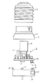
図1は電球形蛍光ランプの一部を切り欠いて示す側面で、図2は電球形蛍光ランプのカバーおよび口金を示す拡大分解側面図で、図3はインバータ回路部分を拡大して示す斜視図である。
【0033】
図1において、は電球形蛍光ランプで、この電球形蛍光ランプ1は、口金2を有するカバー4と、このカバー4に収納された放電灯点灯装置としてのインバータ回路6と、透光性を有するグローブ7と、このグローブ7に収納された放電ランプとしての発光管8とのそれぞれを備えている。また、口金2、カバー4およびグローブ7から構成される外囲器は、定格電力が例えば60Wタイプや100Wタイプの白熱電球などの一般照明用電球の規格寸法に近似する外形に形成されている。なお、一般照明用電球とはJIS C 7501に定義されるものである。
【0034】
また、カバー4は、ポリブチレンテレフタレート(PBT)などの耐熱性合成樹脂などにて形成されたカバー本体11を備えている。このカバー本体11は、下方に拡開する開口部を有する略円筒状に形成されており、エジソンタイプのE26形などの口金2が上端部に被せられて、接着剤またはかしめなどにより固定されている。
【0035】
さらに、グローブ7は、透明あるいは光拡散性を有する乳白色などであり、ガラスあるいは合成樹脂により、白熱電球などの一般照明用電球のガラス球と略同一形状の滑らかな曲面状に形成されている。また、このグローブ7の開口部の縁部には、カバー4の下端開口部の内側に嵌合する図示しない嵌合縁部が形成されている。なお、このグローブ7は、拡散膜などの別部材を組み合わせ、輝度の均一性を向上させることでき、あるいは省略させることもできる。
【0036】
また、インバータ回路6は、水平状、すなわち発光管8の長手方向と垂直に配置される回路基板14を備えている。インバータ回路6は、電解コンデンサ15に対して並列に、スイッチング素子である互いに相補形に構成された一対のNチャネルおよびPチャネルのMOS形電界効果トランジスタ(FET)が直列に接続されたハーフブリッジインバータを構成しいている。
【0037】
この回路基板14には、点灯部品13が実装されている。回路基板14の発光管8に対向する一面には、接続ピンとしてのラッピングピン16が発光管8方向に突出するように設けられている。ラッピングピン16の先端部は、回路基板14の水平方向であって、外側に向くように約90°の角度で接曲されている。
【0038】
回路基板14の他面(口金2側)には、比較的熱に弱く、すなわち比較的耐熱性が低い電解コンデンサなどの回路部品15が配置されている。点灯部品13の一面には、ラッピングピン16の他に比較的耐熱性の高い整流ダイオードチップ等のチップ部品17が実装されている。
【0039】
発光管8の内面には、蛍光体が塗布された図示しない蛍光体層が形成されている。また、発光管8の内部には、アルゴンなどの希ガスや水銀などを含む放電ガスとなる封入ガスが封入されている。
【0040】
発光管8は、略U字状に形成された略同形状の3本の管体を有しており、これら管体の中間部の各管体の両端と、両端の各管体の一端とがつなぎ部となる図示しない連通管部を介して順次接続されて1本の連続した放電路が発光管8内に形成されている。
【0041】
発光管8が形成する放電路の両端には、図示しない一対の電極が封装されており、この電極からリードワイヤ18が導出されている。リードワイヤ18は、回路基板14のラッピングピンに巻き付けることで接続され、発光管8とインバータ回路6とが電気的に接続される。
【0042】
発光管8は、放電ランプ固定部材であり点灯回路固定部材である支持手段としての有底筒状の仕切板31に取り付けられている。また、この仕切板31はカバー4に固定されている。そして、この仕切板31は、円板状をなす基板部32を備えており、この基板部32に発光管8の端部を挿入したうえで接着剤にて接着などして、発光管8が仕切板31に固定されている。
【0043】
そして、この仕切板31をカバー4の内側に嵌合し、さらに、この仕切板31とカバー4との間にグローブ7の嵌合縁部を嵌合した状態で、これら仕切板31とカバー4との間に接着剤を充填することにより、これら仕切板31とカバー4とが互いに固定されている。また、この仕切板31の上側には、取付片部34が突設されている。この取付片部34には、嵌合あるいは接着などされて点灯回路6の回路基板14が取り付けられている。
【0044】
仕切板31の側面のラッピングピン16に対応する位置には、開口35が設けられている。取付片部34が突設されている。この取付片部34に嵌合されて点灯回路6の回路基板14が取り付けられるとともに、取付片部34を利用して仕切板31がカバー体11の内面に取着される。
【0045】
次に、本実施形態の作用について説明する。電球形蛍光ランプ1の組み立てにおいて、まず仕切板31にインバータ回路6を取付け、インバータ回路6と口金2とをリード線などで電気的に接続した後、仕切板31をカバー本体11に取着する。このとき、インバータ回路16の放熱作用を高めるために、カバー本体11内にシリコーン樹脂などの絶縁性放熱材料を充填しても良い。
【0046】
次に、発光管8のリードワイヤ18を仕切板31の開口35から導出させた状態で、発光管8を仕切板31の所定の取付け孔に取着し、固定する。そして、リードワイヤ18をラッピングピン16に接続するときに、ラッピング用の治具を開口35から挿入し、リードワイヤ18をラッピングピン16に巻き付けて接続する。最後にグローブ7をカバー4に取付けて、電球形蛍光ランプ1の組立ては完了する。
【0047】
本実施形態の電球形蛍光ランプ1は、電子部品13が多く実装されない回路基板14の他面側にラッピングピン16が設けられるので、回路基板14の実装スペースが効率的に使用され、インバータ回路6の小形化が可能になる。
【0048】
また、リードワイヤ18が発光管8の電極と接続されているため、リードワイヤ18を介して発光管8の熱がラッピングピン16に伝導し、ラッピングピン16の温度が高くなることがあっても、ラッピングピン16が回路基板14の一面側に設けられているので、ラッピングピン16の温度上昇によって主として他面側へ実装された電子部品13に熱的に影響を及ぼすことが防止される。
【0049】
さらに、ラッピングピン16の先端が回路基板14の一面とほぼ平行になるように折曲されているので、インバータ回路6の高さ方向の寸法を小さくすることができる。また、ラッピングピン16の先端が回路基板14の外側方向を向くように折曲されているので、ラッピングピン16に対してリードワイヤ18を接続するときに、ラッピング用の治具を仕切板31の側方から挿入可能となり、発光管8をカバー1側に仮固定した状態で接続作業を行うことが可能となる。
【0050】
次に、本発明の他の実施形態を図4を参照して説明する。図4に示す実施形態の電球形蛍光ランプは、接続ピン16以外の構成は図1に示す実施形態と同一であるので、同一構成の詳細な説明は省略する。
【0051】
図4は、本発明の他の実施形態の電球形蛍光ランプのインバータ回路部分を示す拡大側面図である。本実施形態の接続ピン16は、回路基板14の他面に実装された電子部品13のリード線を一面側に突出させて形成されている。
【0052】
本実施形態によれば、電子部品13のリード線を一面側に突出させて接続ピン16としているので、別個に接続ピンを必要とすることが無く、部品点数を削減することができるという効果を有する。
【0053】
【発明の効果】
本発明によれば、インバータ回路の電子部品があまり多く実装されていない回路基板の一面に接続ピンが設けられているので、接続ピンを回路基板に効率的に配設することができ、インバータ回路を小形化することができる。また、リードワイヤが放電ランプの電極と接続されている場合に接続ピンが温度上昇しても、他面側に実装された電子部品へ熱的に影響を及ぼすことが防止される。
【図面の簡単な説明】
【図1】本発明の一実施形態の電球形蛍光ランプの一部を切り欠いて示す側面。
【図2】図1の電球形蛍光ランプのカバーおよび口金を示す拡大分解側面図。
【図3】図1のインバータ回路部分を拡大して示す斜視図。
【図4】本発明の他の実施形態の電球形蛍光ランプのインバータ回路部分を示す拡大側面図。
【符号の説明】
1…電球形蛍光ランプ、2…口金、4…カバー、8…放電ランプとしての発光管、6…インバータ回路、16…接続ピンとしてのラッピングピン、18…リードワイヤ。[0001]
BACKGROUND OF THE INVENTION 1. Field of the Invention The present invention relates to a bulb-type fluorescent lamp provided with an inverter circuit having a circuit board provided with connection pins connected to lead wires derived from a discharge lamp.
[0002]
[Prior art]
The bulb-type fluorescent lamp has a lighting circuit for lighting the discharge lamp, and since the inverter circuit has been used in this lighting circuit, the compact and high efficiency of the bulb-type fluorescent lamp has been promoted, and the incandescent lamp has been developed. The replacement with a compact fluorescent lamp has been further promoted.
[0003]
However, with the miniaturization of compact fluorescent lamps, the temperature inside the cover tends to increase during lighting, and measures such as improving the heat resistance of the electronic components that make up the inverter circuit, which are easily affected by heat, are taken. Was needed.
[0004]
In order to reduce the thermal effects on the circuit components, mount the high heat-resistant components on one side of the circuit board facing the discharge lamp, and mount the low heat-resistant electronic components on the other side on the opposite side. 2. Description of the Related Art A bulb-type fluorescent lamp including an inverter circuit on which components are mounted is known (for example, see Patent Document 1). In this conventional bulb-type fluorescent lamp, since the heat of the discharge lamp is blocked by the circuit board and the temperature inside the cover on the other side is lower than that on one side, the heat resistance of an electrolytic capacitor etc. By mounting an electronic component having a low temperature, thermal effects on circuit components are suppressed.
[0005]
[Patent Document 1]
JP 2000-173536 A
[Problems to be solved by the invention]
However, miniaturization and high output of the bulb-type fluorescent lamp are further progressing, and it is difficult to sufficiently suppress the thermal effect only by the mounting structure of the electronic component like the above-mentioned conventional bulb-type fluorescent lamp. ing. In particular, the temperature of the connection pins mounted on the circuit board may increase, and it is necessary to prevent the heat radiated from the connection pins from affecting the electronic components. The rise in the temperature of the connection pin is due to the fact that the heat of the discharge lamp is transmitted to the connection pin by heat conduction via a lead wire connected to the connection pin.
[0007]
On the other hand, a connection pin to which a lead wire derived from a discharge lamp of a bulb-shaped fluorescent lamp is connected is mounted on a circuit board, and this connection pin is connected to the other side of the circuit board on which most of the electronic components are mounted. Therefore, it is necessary to reduce the size of the connection pins in order to secure a space for mounting the circuit board on the other side.
[0008]
SUMMARY OF THE INVENTION The present invention has been made in view of the above circumstances, and a light bulb that can reduce the influence of heat radiated from a connection pin, suppress the heat influence on electronic components, and reduce the size of an inverter circuit. It is an object of the present invention to provide a shaped fluorescent lamp.
[0009]
[Means for Solving the Problems]
The bulb-type fluorescent lamp according to claim 1 includes a discharge lamp; a connection pin connected to a lead wire derived from the discharge lamp; and a circuit board on which electronic components constituting a high-frequency lighting circuit for lighting the discharge lamp are mounted. An inverter circuit provided on one side of the circuit board facing the discharge lamp; a cover supporting the discharge lamp and accommodating the inverter circuit; and a base attached to the cover. It is characterized by doing.
[0010]
In this claim and the following claims, the definitions of terms are as described below.
[0011]
The discharge lamp has an arc tube, is formed by bending a straight tubular bulb, and has at least one discharge path formed therein in parallel to communicate a plurality of U-shaped bent bulbs. In addition to the above, an arc discharge tube of an electrodeless discharge type constituted by a hollow rotating body may be used. In the case of an arc tube in which a discharge path is formed, an electrode for generating a discharge is sealed at an end of the discharge path. Examples of the electrode include a hot cathode composed of a filament, a ceramic electrode carrying an electron-emitting substance, and a cold cathode formed of nickel or the like.
[0012]
The arc tube is preferably made of glass such as lead glass, soda lime glass, borosilicate glass or the like, but other materials such as ceramics may be used as long as they are translucent. In particular, considering the effect on the environment, it is optimal to form with lead-free glass. Lead-free glass is glass that does not substantially contain lead, and may contain lead of an impurity level. For example, Na 2 O is 0 to 10 mass%, K 2 O is 1 to 10 mass%, Li 2 O 0 to 3 wt% (provided that the total amount of Na 2 O, K 2 O and Li 2 O 5 -20% by mass) and a glass having a softening temperature of 685 ° C or lower. Glass using K 2 O and Li 2 O together with Na 2 O as a flux has a composition substantially free of lead and can lower the softening temperature to 685 ° C. or lower as compared with conventional soda-lime glass. . By applying such a glass having a low softening point to a glass bulb, the heating temperature at the time of bulb processing can be reduced, and based on the decrease in the heating temperature, thermal degradation of the phosphor layer and, consequently, reduction of the total luminous flux. Can be suppressed. Further, by setting the amount of Na 2 O to 10% by mass or less, it becomes possible to suppress coloring caused by the Na component in the glass and, consequently, decrease in the luminous flux maintenance factor.
[0013]
A phosphor layer may be directly or indirectly applied to the inner surface of the arc tube of the discharge lamp. As the phosphor, a three-wavelength emission type rare earth metal oxide phosphor, a calcium halophosphate phosphor, or the like can be used. In addition, an inert gas such as argon, neon, or krypton, or a discharge medium such as mercury or xenon gas is sealed inside the arc tube. The arc tube may use a rare gas discharge that does not encapsulate mercury or may have an electrode outside.
[0014]
When mercury is sealed in the arc tube, it is preferable to seal amalgam, but not limited to this. The amalgam may have a characteristic that the vapor pressure is higher than that of pure mercury sealed for efficient lighting even at high temperature, or may be used for quantitatively sealing mercury in the bulb. In particular, when the lamp is turned on, the arc tube becomes hot. Therefore, it is necessary to select an amalgam having a vapor pressure characteristic corresponding to the lighting temperature. Examples of amalgam considering vapor pressure characteristics include bismuth (Bi) -indium (In) -mercury (Hg), bismuth (Bi) -tin (Sn) -lead (Pb) -mercury (Hg), and bismuth (Bi). ) -Indium (In) -Lead (Pb) -Mercury (Hg), but are not limited thereto. Examples of the amalgam for quantitative encapsulation include, but are not limited to, zinc (Zn) -mercury (Hg). In addition, although not amalgam, a pellet in which mercury is supported on a substance such as ceramics may be held in the thin tube.
[0015]
The arc tube can be formed by connecting a plurality of tubular bulbs bent in a U-shape so as to communicate with one discharge path. Therefore, it is allowed to use arc tubes having various shapes such as double U, triple U, and four U. In the case of a double U-shaped arc tube, an electrode is sealed at one end of a U-shaped bulb and the other end is connected to form an electric discharge between the electrodes sealed at each end of the two tubular bulbs. It will be. In the case of a triple U-shaped arc tube, an electrode is sealed at one end of two U-shaped bulbs, and the other end is connected to the end of an intermediate bulb where the electrode is not sealed, thereby forming three tubular bulbs. A discharge is generated between the electrodes sealed at one end of each of the U-shaped bulbs on both sides. In the case of four U, a plurality of U-shaped bent tubular valves can be arranged side by side so as to be parallel to each other. Regardless of the case of double U, triple U, or four U, the place where the thin tube is sealed may be either the end where the electrode is sealed or the end formed by connecting. Further, the sealing of the thin tube may be performed by either a stem seal or a pinch seal.
[0016]
A lead wire for power supply is led out of the discharge lamp, and this lead wire is wound around a connection pin of the inverter circuit and connected by means such as welding or caulking. The lead wire is connected to this electrode when the arc tube is sealed with an electrode, and is connected to an electromagnetic field generating means such as a coil in the case of an electrodeless discharge lamp. It is.
[0017]
The cover directly or indirectly supports the arc tube of the discharge lamp. As means for indirectly supporting the arc tube, it is preferable to mount a holder having a shape capable of attaching the arc tube of the discharge lamp to a portion of the cover opposite to the direction in which the base is attached. This holder may be either integral with or separate from the cover. Further, the holder can have a blocking action so that radiant heat or ultraviolet rays from the arc tube does not reach the inverter circuit inside the cover.
[0018]
The cover has a base, and is configured such that the entire bulb-type fluorescent lamp has a height of 75 to 140 mm including the base. A glove covering the discharge lamp may be attached to the cover. This glove may be light-diffusing or transparent as long as it has light-transmitting properties, and may be patterned or colored. The material of the glove may be either glass or plastic. The shape of the globe is arbitrary, but a so-called A-shape similar to a commonly used incandescent lamp, a so-called G-shape similar to a sphere, and a so-called T-shape with a spherical tip and a cylindrical shape. A so-called shape or the like can be adopted. The overall height of the bulb-type fluorescent lamp when the glove is attached is defined by the height including the glove.
[0019]
The inverter circuit mainly includes an electronic component for applying a high frequency power of 10 kHz or more to the discharge lamp to light the discharge lamp, and the electronic component and the above-described connection pins are mounted on a circuit board. The circuit board is large enough to be disposed inside the cover such that one surface of the circuit board faces the discharge lamp, and has a circular or polygonal shape. In addition, most of the electronic components mounted on the circuit board are mounted on the other surface, which is the surface opposite to the surface facing the discharge lamp, but a part is mounted on one surface of the circuit board. May be.
[0020]
Connection pins are provided on one surface side of the circuit board. The connection pins need to have a relatively large mounting space because it is necessary to secure a space around the connection pins for inserting the wrapping or welding jig during the connection work. There is. Therefore, the connection pins must be efficiently arranged on the circuit board. However, on one side of the circuit board, the electronic components are not mounted much more than on the other side, so that a mounting space is secured. be able to.
[0021]
When the lead wire is connected to the electrode of the discharge lamp, heat of the discharge lamp is conducted to the connection pin via the lead wire, and the temperature of the connection pin may increase. However, since the connection pins are provided on one side of the circuit board, even if the temperature of the connection pins rises, it is possible to prevent the electronic components mounted on the other side from being thermally affected.
[0022]
On one surface side of the circuit board, in addition to the connection pins, an electronic component whose characteristics do not significantly change even when affected by heat from the arc tube may be mounted. For example, winding parts such as a choke ballast and a transformer, a transistor, a diode, a resistor, and the like can be given.
[0023]
As the base, a screw-in type called an E shape is usually used, but the present invention is not limited to this as long as it can be attached to a socket to which an incandescent lamp is mounted. The base does not need to be directly attached to the cover, but may be indirectly attached to the case or a part of the cover may constitute the base.
[0024]
According to the first aspect of the present invention, since the connection pins are provided on one surface of the circuit board on which the electronic components of the inverter circuit are not mounted so much, the connection pins can be efficiently arranged on the circuit board. In addition, the inverter circuit can be downsized. Further, even when the temperature of the connection pin rises when the lead wire is connected to the electrode of the discharge lamp, it is possible to prevent the electronic components mounted on the other surface from being thermally affected.
[0025]
According to a second aspect of the present invention, in the light bulb-shaped fluorescent lamp according to the second aspect, the connection pin protrudes from one surface of the circuit board, and is bent so that its tip is substantially parallel to the one surface of the circuit board. .
[0026]
According to the second aspect of the present invention, since the tip of the connection pin is bent so as to be substantially parallel to one surface of the circuit board, the height dimension of the inverter circuit can be reduced.
[0027]
According to a third aspect of the present invention, in the bulb-type fluorescent lamp according to the first or second aspect, the connection pin is bent so that the tip thereof is directed to the outside of the circuit board, and the lead wire is wound around the connection pin and connected. Features that have.
[0028]
According to the invention of claim 3, when the lead wire is connected to the connection pin, a jig for wrapping or welding can be inserted from the side, for example, in a state where the discharge lamp is temporarily fixed to the cover side. Connection work can be performed.
[0029]
According to a fourth aspect, in the light-bulb-shaped fluorescent lamp according to any one of the first to third aspects, the connection pin is formed by projecting a lead wire of an electronic component mounted on the other surface of the circuit board to one surface side. It is characterized by the following.
[0030]
According to the fourth aspect of the present invention, since the lead wire of the electronic component is formed as a connection pin by protruding to one surface side, no separate connection pin is required, and the number of components can be reduced.
[0031]
BEST MODE FOR CARRYING OUT THE INVENTION
Hereinafter, one embodiment of a bulb-type fluorescent lamp of the present invention will be described with reference to the drawings.
[0032]
1 is a partially cutaway side view of a light bulb shaped fluorescent lamp, FIG. 2 is an enlarged exploded side view showing a cover and a base of the light bulb shaped fluorescent lamp, and FIG. 3 is an enlarged perspective view showing an inverter circuit portion. It is.
[0033]
In FIG. 1, is a bulb-type fluorescent lamp, and the bulb-type fluorescent lamp 1 has a
[0034]
The
[0035]
Further, the
[0036]
In addition, the
[0037]
The
[0038]
On the other surface of the circuit board 14 (the
[0039]
On the inner surface of the
[0040]
The
[0041]
At both ends of the discharge path formed by the
[0042]
The
[0043]
Then, the
[0044]
An
[0045]
Next, the operation of the present embodiment will be described. In assembling the bulb-type fluorescent lamp 1, first, the
[0046]
Next, with the lead wire 18 of the
[0047]
In the bulb-type fluorescent lamp 1 of the present embodiment, the wrapping pins 16 are provided on the other surface of the
[0048]
Further, since the lead wire 18 is connected to the electrode of the
[0049]
Furthermore, since the tip of the
[0050]
Next, another embodiment of the present invention will be described with reference to FIG. The configuration of the bulb-type fluorescent lamp of the embodiment shown in FIG. 4 is the same as that of the embodiment shown in FIG. 1 except for the connection pins 16, and a detailed description of the same configuration will be omitted.
[0051]
FIG. 4 is an enlarged side view showing an inverter circuit portion of a bulb-type fluorescent lamp according to another embodiment of the present invention. The
[0052]
According to the present embodiment, since the
[0053]
【The invention's effect】
According to the present invention, since the connection pins are provided on one surface of the circuit board on which the electronic components of the inverter circuit are not mounted so much, the connection pins can be efficiently arranged on the circuit board, and the inverter circuit Can be miniaturized. Further, even if the temperature of the connection pin rises when the lead wire is connected to the electrode of the discharge lamp, it is possible to prevent the electronic components mounted on the other surface from being thermally affected.
[Brief description of the drawings]
FIG. 1 is a partially cutaway side view of a bulb-type fluorescent lamp according to an embodiment of the present invention.
FIG. 2 is an enlarged exploded side view showing a cover and a base of the compact fluorescent lamp of FIG. 1;
FIG. 3 is an enlarged perspective view showing an inverter circuit part of FIG. 1;
FIG. 4 is an enlarged side view showing an inverter circuit portion of a bulb-type fluorescent lamp according to another embodiment of the present invention.
[Explanation of symbols]
DESCRIPTION OF SYMBOLS 1 ... Light bulb type fluorescent lamp, 2 ... Base, 4 ... Cover, 8 ... Arc tube as discharge lamp, 6 ... Inverter circuit, 16 ... Wrapping pin as connection pin, 18 ... Lead wire.
Claims (4)
この放電ランプから導出されたリードワイヤと接続される接続ピン、放電ランプを点灯させる高周波点灯回路を構成する電子部品が実装された回路基板を有し、接続ピンが回路基板の放電ランプに対向する側の一面に設けられたインバータ回路と;
放電ランプを支持するとともにインバータ回路が収容されたカバーと;
カバーに取り付けられた口金と;
を具備していることを特徴とする電球形蛍光ランプ。A discharge lamp;
A connection pin connected to a lead wire derived from the discharge lamp, a circuit board on which electronic components constituting a high-frequency lighting circuit for lighting the discharge lamp are mounted, and the connection pin faces the discharge lamp of the circuit board An inverter circuit provided on one side of the side;
A cover for supporting the discharge lamp and containing the inverter circuit;
A base attached to the cover;
A bulb-type fluorescent lamp comprising:
Priority Applications (1)
| Application Number | Priority Date | Filing Date | Title |
|---|---|---|---|
| JP2003097380A JP2004303662A (en) | 2003-03-31 | 2003-03-31 | Compact self-ballasted fluorescent lamp |
Applications Claiming Priority (1)
| Application Number | Priority Date | Filing Date | Title |
|---|---|---|---|
| JP2003097380A JP2004303662A (en) | 2003-03-31 | 2003-03-31 | Compact self-ballasted fluorescent lamp |
Publications (1)
| Publication Number | Publication Date |
|---|---|
| JP2004303662A true JP2004303662A (en) | 2004-10-28 |
Family
ID=33409183
Family Applications (1)
| Application Number | Title | Priority Date | Filing Date |
|---|---|---|---|
| JP2003097380A Withdrawn JP2004303662A (en) | 2003-03-31 | 2003-03-31 | Compact self-ballasted fluorescent lamp |
Country Status (1)
| Country | Link |
|---|---|
| JP (1) | JP2004303662A (en) |
-
2003
- 2003-03-31 JP JP2003097380A patent/JP2004303662A/en not_active Withdrawn
Similar Documents
| Publication | Publication Date | Title |
|---|---|---|
| US7053554B2 (en) | Bulb-shaped fluorescent lamp and illumination device | |
| JP4126527B2 (en) | Light bulb shaped fluorescent lamp | |
| JP2005347236A (en) | Compact self-ballasted fluorescent lamp, and illumination device | |
| JP4099702B2 (en) | Light bulb-type fluorescent lamp and lighting device | |
| JP2004303662A (en) | Compact self-ballasted fluorescent lamp | |
| JP4139997B2 (en) | Light bulb shaped fluorescent lamp and lighting fixture | |
| JP2003059452A (en) | Compact self-ballasted fluorescent lamp and luminaire | |
| JP4304605B2 (en) | Light bulb-type fluorescent lamp and lighting device | |
| JP3861602B2 (en) | Light bulb-type fluorescent lamp and lighting fixture | |
| JP4822078B2 (en) | Light bulb-type fluorescent lamp and lighting fixture | |
| JP4221654B2 (en) | Light bulb-type fluorescent lamp and lighting device | |
| JP4196668B2 (en) | Light bulb shaped fluorescent lamp and lighting fixture | |
| JP4310676B2 (en) | Fluorescent lamps and lighting fixtures | |
| JP2003059307A (en) | Bulb shaped fluorescent lamp and luminaire | |
| JP2000353403A (en) | Fluorescent lamp device | |
| JP2007273264A (en) | Self-ballasted fluorescent lamp and lighting system | |
| JP2006012559A (en) | Fluorescent lamp device and lighting fixture | |
| JP2003203607A (en) | Fluorescent lamp and bulb-shaped fluorescent lamp | |
| JP2000106134A (en) | Fluorescent lamp and bulb type fluorescent lamp | |
| JP3778278B2 (en) | Light bulb shaped fluorescent lamp | |
| JP2001283607A (en) | Electric bulb type fluorescent lamp | |
| JP2004030963A (en) | Compact selfbalasted fluorescent lamp | |
| JP2006114224A (en) | Fluorescent lamp, compact self-ballasted fluorescent lamp, and lighting apparatus | |
| JP2004288385A (en) | Electrodeless fluorescent lamp, electrodeless self-ballasted compact fluorescent lamp, and lighting device | |
| JP2002231007A (en) | Fluorescent lamp device and bulb-type fluorescent lamp |
Legal Events
| Date | Code | Title | Description |
|---|---|---|---|
| A621 | Written request for application examination |
Free format text: JAPANESE INTERMEDIATE CODE: A621 Effective date: 20060214 |
|
| A761 | Written withdrawal of application |
Free format text: JAPANESE INTERMEDIATE CODE: A761 Effective date: 20070216 |