JP2004282921A - Power supply rack and power supply - Google Patents
Power supply rack and power supply Download PDFInfo
- Publication number
- JP2004282921A JP2004282921A JP2003071985A JP2003071985A JP2004282921A JP 2004282921 A JP2004282921 A JP 2004282921A JP 2003071985 A JP2003071985 A JP 2003071985A JP 2003071985 A JP2003071985 A JP 2003071985A JP 2004282921 A JP2004282921 A JP 2004282921A
- Authority
- JP
- Japan
- Prior art keywords
- power supply
- switch
- converter
- smoothing capacitor
- rack
- Prior art date
- Legal status (The legal status is an assumption and is not a legal conclusion. Google has not performed a legal analysis and makes no representation as to the accuracy of the status listed.)
- Pending
Links
Images


Abstract
Description
【0001】
【発明の属する技術分野】
本発明は、AC/DC変換部と複数のDC/DC変換部をユニット化して構成された電源ラックにおいて、前記DC/DC変換部等のメインテナンス時に、作業者の感電事故を未然に防ぐのに好適な電源ラック、及び電源に関する。
【0002】
【従来の技術】
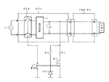
図8は、パワー・ディストリビューション・ユニットPDU(AC/DC変換部)と複数のパワー・モジュールPMa〜PMn(DC/DC変換部)をユニット化して構成される従来の電源ラックの回路図である。また、図9は、図8に示す電源ラックを示す斜視図である。以下の説明では、発明の属する技術分野において述べた前記AC/DC変換部をパワー・ディストリビューション・ユニットPDUと称し、DC/DC変換部をパワー・モジュールPMと称するものとする。
【0003】
図8と図9から明らかなように、パワー・ディストリビューション・ユニットPDUと複数のパワー・モジュールPMa〜PMnは、パワーサプライ・バックプレインPWR BP(Power Supply Buck Plane :電源基板)に着脱可能に構成されている。
パワー・ディストリビューション・ユニットPDUは、交流電源1から出力される交流電流を、ノン・ヒューズ・ブレーカNFBを介して、整流回路2において整流し、平滑用コンデンサCにより平滑して、パワーサプライ・バックプレインPWR BPに電力を供給している。
【0004】
パワーサプライ・バックプレインPWR BPは、複数のパワー・モジュールPMa,PMb〜PMnを備えている。各パワーモジュールPMa〜PMnは、パワーサプライ・バックプレインPWR BPから受けた直流電圧を所定の電圧に変換して図示しない各々の負荷に供給している。ここで、パワー・モジュールPMa〜PMnは、パワー・ディストリビューション・ユニットPDUから供給される直流電圧が高い場合、通常、絶縁型DC/DCコンバータが用いられる。
【0005】
【特許文献1】
特開平9−283189号公報(第2頁)
【0006】
【発明が解決しようとする課題】
図8に示す電源ラックには、次のような問題点がある。
【0007】
図8に示す電源ラックにおいて、作業者がそのメインテナンスを行う場合、パワー・ディストリビューション・ユニットPDU内の平滑用コンデンサCに蓄積された電荷に起因する感電事故を未然に防ぐ必要がある。
パワー・ディストリビューション・ユニットPDUをオフにした場合、平滑用コンデンサCに蓄積された電荷は、抵抗Rを通して放電され、作業者の感電事故が防止される。
【0008】
しかし、抵抗Rを通しての放電は、発熱の問題、及び実装スペースの問題に起因して、短時間での放電が困難である。したがって、作業者は、放電が終了したと勘違いして、感電事故に遇う危険性がある。
また、抵抗Rには、電源ラックの運転時に、常に、電流が流れるため、パワー・ディストリビューション・ユニットPDUの運転時における部品発熱の問題、及び内部損失の問題にも直結する。
【0009】
また、前記部品発熱の問題、及び内部損失の問題は、パワー・ディストリビューション・ユニットPDUから電力を受けて動作するパワー・モジュールにおいても問題になる。
【0010】
本発明は、前記した従来技術の問題点に鑑み為されたもので、電源ラックのメインテナンス時等において、平滑用コンデンサの蓄積電荷を急速に放電することを可能にし、作業者が感電事故を起こすのを防止するのに適した電源ラックを提供することにある。
本発明の他の目的は、電源ラックの運転時に、パワー・ディストリビューション・ユニットやパワー・モジュールにおける部品発熱及び内部損失を低減するのに適した電源ラックを提供することにある。
【0011】
本発明の他の目的は、電源内部の整流平滑部に設けられた平滑用コンデンサの蓄積電荷を急速に放電することを可能にし、作業者が感電事故を起こすのを防止するのに適した電源を提供することにある。
本発明の他の目的は、部品発熱及び内部損失を低減することが可能な電源を提供することにある。
【0012】
【課題を解決するための手段】
請求項1に記載の電源ラックは、AC/DC変換部と複数のDC/DC変換部をユニット化して構成される電源ラックにおいて、前記AC/DC変換部に設けられ、前記AC/DC変換部に入力されているAC入力が遮断されたとき開閉動作を行う補助スイッチを有するノン・ヒューズ・ブレーカと、ノン・ヒューズ・ブレーカの補助スイッチの開閉動作に応じて、AC/DC変換部に設けられた平滑用コンデンサに蓄積されている電荷を強制的に放電させる放電回路とを備えたことを特徴とする。
【0013】
請求項2に記載の電源ラックは、請求項1記載の電源ラックにおいて、前記補助スイッチの代わりに、前記AC/DC変換部が故障したとき、前記AC/DC変換部から出力される内部エラー信号によって開閉動作を行うスイッチを有することを特徴とする。
【0014】
請求項3記載の電源ラックは、請求項1記載の電源ラックにおいて、前記補助スイッチの代わりに、前記AC/DC変換部に入力されているAC入力が遮断されたとき、前記AC/DC変換部から出力される停電検出信号によって開閉動作をするスイッチを有することを特徴とする。
請求項4記載の電源ラックは、AC/DC変換部と複数のDC/DC変換部をユニット化し構成される電源ラックにおいて、前記AC/DC変換部から通常運転状態又は運転停止状態を示すドライブ信号が出力されたとき、前記ドライブ信号が通常運転状態を示すとき第1の状態に設定され、前記ドライブ信号が運転停止状態を示すとき第2の状態に設定されるスイッチと、前記スイッチが第2の状態に設定されたとき、AC/DC変換部に設けられた平滑用コンデンサに蓄積されている電荷を放電させる放電回路とを備えたことを特徴とする。
【0015】
請求項5記載の電源ラックは、AC/DC変換部と複数のDC/DC変換部をユニット化して構成される電源ラックにおいて、前記AC/DC変換部と前記複数のDC/DC変換部を着脱可能な基板と、前記基板から前記AC/DC変換部を引き抜くことにより、前記AC/DC変換部に設けられたスイッチを開動作させるスイッチ開回路と、前記スイッチの開動作に応じて、前記AC/DC変換部に設けられた平滑用コンデンサに蓄積されている電荷を強制的に放電させる放電回路とを備えたことを特徴とする。
【0016】
請求項6記載の電源ラックは、請求項1から請求項5のいずれか一つに記載の電源ラックにおいて、前記放電回路は、前記スイッチとして大電流を流すことが可能なスイッチを有することを特徴とする。
請求項7記載の電源は、AC/DC変換部を備えた電源において、AC/DC変換部内に設けられた平滑整流部に存在する平滑用コンデンサに蓄積された電荷を放電させる請求項1に記載の補助スイッチと放電回路を備えたことを特徴とする。
【0017】
請求項8に記載の電源は、AC/DC変換部を備えた電源において、AC/DC変換部内に設けられた平滑整流部に存在する平滑用コンデンサに蓄積された電荷を放電させる請求項2乃至請求項3のいずれか一つに記載のスイッチと放電回路を備えたことを特徴とする。
請求項9記載の電源は、AC/DC変換部を備えた電源において、AC/DC変換部内に設けられた平滑整流部に存在する平滑用コンデンサに蓄積された電荷を放電させる請求項4に記載のスイッチとスイッチ開回路と放電回路を備えたことを特徴とする。
【0018】
請求項10に記載の電源は、AC/DC変換部を備えた電源において、AC/DC変換部内に設けられた平滑整流部に存在する平滑用コンデンサに蓄積された電荷を放電させる請求項5に記載のスイッチとスイッチ開回路と放電回路を備えたことを特徴とする。
請求項11に記載の電源は、AC/DC変換部を備えた電源において、AC/DC変換部内に設けられた平滑整流部に存在する平滑用コンデンサに蓄積された電荷を放電させるスイッチング素子と抵抗の直列回路と、AC/DC変換部から運転停止を示す信号が出力されたとき動作し、前記抵抗と前記スイッチング素子の間の電圧を検出して、検出された電圧が所定の値になるようにスイッチング素子をオン/オフ制御する制御手段とを有していることを特徴とする。
【0019】
請求項1から請求項3に記載の電源ラックによれば、補助スイッチと放電回路の働きにより、平滑用コンデンサに蓄積されている電荷を強制的に放電させることができる。
請求項4に記載の電源ラックによれば、スイッチと放電回路の働きにより、AC/DC変換部に存在する平滑用コンデンサに蓄積されている電荷を強制的に放電させることができる。
【0020】
請求項5に記載の電源ラックによれば、スイッチとスイッチ開回路と放電回路の働きにより、平滑整流部に存在する平滑用コンデンサに蓄積されている電荷を強制的に放電させることができる。
【0021】
請求項6に記載の電源ラックによれば、スイッチと放電回路の働きにより、平滑整流部に存在する平滑用コンデンサに蓄積されている電荷を強制的に放電させることができる。
請求項7に記載の電源によれば、補助スイッチと放電回路の働きにより、平滑整流部に存在する平滑用コンデンサに蓄積されている電荷を強制的に放電させることができる。
【0022】
請求項8に記載の電源によれば、スイッチと放電回路の働きにより、平滑整流部に存在する平滑用コンデンサに蓄積されている電荷を強制的に放電させることができる。
請求項9に記載の電源によれば、スイッチとスイッチ開回路と放電回路の働きによりにより、平滑整流部に存在する平滑用コンデンサに蓄積されている電荷を強制的に放電させることができる。
【0023】
請求項10に記載の電源によれば、スイッチとスイッチ開回路とスイッチ開回路と放電回路の働きによりにより、平滑整流部に存在する平滑用コンデンサに蓄積されている電荷を強制的に放電させることができる。
請求項11に記載の電源によれば、前記直列回路に流れる電流をリニアに制御することができるので、直列回路内のスイッチング素子において主に電力消費を行い、直列回路内の抵抗による電力消費を小さくすることができる。したがって、AC/DC変換部に設けられている平滑用コンデンサに蓄積されている電荷を強制的に放電させることを可能にするとともに、抵抗とスイッチング素子の直列回路から構成される放電回路が溶断することを防止することができる。
【0024】
【発明の実施の形態】
以下、本発明の実施の形態について説明する。
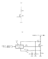
図1は、本発明の第1の実施の形態を示す回路図である。図1において、従来技術と同一部分には同一符号を付して、その説明を省略する。なお、第1の実施の形態は、請求項1〜3に対応している。
【0025】
図1に示す第1の実施の形態が図8示す従来技術と相違するのは、平滑用コンデンサCの+側に抵抗R1,R2とFETQ1とツェナーダイオードZD1とスイッチSW1から成る回路が設けられていることである。ここで、スイッチSW1は、ノン・ヒューズ・ブレーカNFBの補助スイッチであり、ノン・ヒューズ・ブレーカNFBが遮断されるのと同期してオフされるスイッチである。また、図8に示す従来技術で設けられていた放電用の抵抗Rは、設けられていない。前記抵抗Rに相当するのは、抵抗R1である。また、抵抗R2は十分に大きな抵抗値を有している。
【0026】
以下、図1に示す第1の実施の形態の動作を説明する。
通常動作時においては、ノン・ヒューズ・ブレーカNFBが導通状態にあるので、スイッチSW1はオンしている。したがって、FETQ1のゲートには、スイッチSW1を通してグランド電位が印加され、FETQ1はオフ状態を保持する。このとき、平滑用コンデンサCの蓄積電荷は、抵抗R2が十分大きな抵抗値を有しているので、スイッチSW1を通して放電されることはない。
【0027】
作業者がメインテナンスのために、ノン・ヒューズ・ブレーカNFBを遮断すると、スイッチSW1が連動してオフする。これによって、FETQ1のゲート電位はアース電位からツェナーダイオードZD1のツェナー電圧に遷移し、FETQ1はオンする。したがって、平滑用コンデンサCに蓄積されていた電荷は、抵抗R1→FETQ1を通してグランドへ放電する。このとき、抵抗R1が放電抵抗の役割を果たす。
【0028】
なお、抵抗R2は、スイッチSW1がオンしているとき、抵抗R2とスイッチSW1を介して微小電流を流すために設けられている。また、スイッチSW1がオフしているとき、前記ツェナー電圧を発生させるためにも設けられている。
【0029】
第1の実施の形態によれば、作業者がメインテナンスを行うとき、ノン・ヒューズ・ブレーカNFBを遮断することにより、FETQ1がオンして、平滑用コンデンサCの蓄積電荷を放電することができる。したがって、作業者が感電する事故を防止することが可能になる。また、パワー・ディストリビューション・ユニットやパワー・モジュールにおける部品発熱及び内部損失を低減することが可能になる。
【0030】
なお、FETQ1の代わりに、リレーやトランジスタやIGBT等を用いることも可能である。
さらに、平滑用コンデンサCの容量が大きく、放電電荷量が多い場合には、FETQ1の代わりに、大電流を流すことができるパワーリレーなどの接点を用いればよい。これは、請求項6に対応する。
【0031】
前記した第1の実施の形態においては、ノン・ヒューズ・ブレーカNFBを遮断状態にしてFETQ1をオンさせたが、本実施の形態はこれに限定されるものではない。
例えば、パワー・ディストリビューション・ユニットPDUに入力されているAC入力が遮断されたとき、パワー・ディストリビューション・ユニットPDUは停電検出信号を出力する。この停電検出信号を用いて、スイッチSW1をオフして、FETQ1をオンし、平滑用コンデンサCの蓄積電荷を放電してもよい。
【0032】
さらに、ノン・ヒューズ・ブレーカNFBや交流電源1等が故障したとき出力される内部エラー信号を用いて、スイッチSW1をオフして、FETQ1をオンし、コンデンサCの蓄積電荷を放電してもよい。
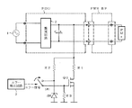
図2は、前記した内部エラー信号を用いた第1の実施の形態の変形例を示す回路図である。すなわち、エラー検出回路3がパワー・ディストリビューション・ユニットPDUの内部エラーや交流電源等の外部エラーを検出し、エラー信号を出力する。スイッチSW1は、エラー信号を受けてオンし、FETQ1がオンする。これにより、コンデンサCの蓄積電荷が放電される。エラー信号としては、前記した停電検出信号も含まれる。これは、請求項2、3に対応する。
【0033】
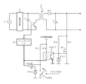
図3は、本発明の第2の実施の形態を示す回路図である。第2の実施の形態は、パワー・ディストリビューション・ユニットPDUをPWM制御により動作させたときの実施の形態である。図3において、従来技術と同一部分には同一符号を付して、その説明を省略する。なお、この実施の形態は請求項4に対応する。
図3に示すように、整流回路2と平滑用コンデンサCによって直流に変換し、さらにスイッチングトランジスタTrによってオン/オフ制御する。これにより、トランスTの二次側に交流が発生する。発生した交流は、ダイオードD1と平滑用コンデンサCによって直流に変換され、図示しないパワーモジュール(PMa等:図8参照)に出力される。
【0034】
平滑用コンデンサCの+側は、図1と同様に抵抗R1,R2,FETQ1,ツェナーダイオードZD1の構成を有している。FETQ1のゲートは、フォトカプラ5のフォトトランジスタのコレクタと接続され、前記フォトトランジスタのエミッタはグランドされている。また、FETQ1のゲートは、ツェナーダイオードZD1を介してグランドされている。
【0035】
他方において、フォトカプラ5の発光ダイオードは、抵抗R4を介して内部補助電源に接続されている。また、内部補助電源は抵抗R5を介してオペアンプOPの+入力端子に接続されている。オペアンプOPの−入力端子は、ツェナーダイオードZD2を介してグランドに接続されている。オペアンプOPの+入力端子は、スイッチSW2を介してグランドに接続可能に形成されている。また、フォトカプラ5のフォトダイオードの出力及びオペアンプOPの出力は、共にスイッチングIC4に入力されている。スイッチングIC4の出力は、スイッチングトランジスタTrのベースに接続されている。
【0036】
ここで、図3に示すドライブ信号は、パワー・ディストリビューション・ユニットPDUから出力され、パワー・ディストリビューション・ユニットPDUがPWM制御により通常運転を行っているときHとなり、パワー・ディストリビューション・ユニットPDUがPWM制御により停止中であるときLとなる信号である。スイッチSW2は前記ドライブ信号を受けて、ドライブ信号がH(通常運転)のときオフし、ドライブ信号がL(運転停止)のときオンする。
【0037】
次に、図3に示す第2の実施の形態の動作について説明する。
通常動作時においては、交流電源1から出力される交流電流は整流回路2において整流され、平滑用コンデンサCにおいて平滑される。また、ドライブ信号はHであるので、スイッチングトランジスタTrはスイッチングIC4の制御により適切にオン/オフ制御される。したがって、トランスTの一次側には交流電流が流れる。その結果、トランスTの二次側に交流電流が発生し、発生した交流電流はダイオードD1と平滑用コンデンサCにより直流に変換される。
【0038】
前記二次側の直流出力は、一方において、パワーサプライ・バックプレインPWR BPを介して、パワーモジュールPMに入力される(図1参照)。また、前記直流出力は、他方において、抵抗R1,R2,FETQ1,ツェナーダイオードZD1、フォトカプラ5から成る回路に入力される。
このとき、前記スイッチSW2はドライブ信号(Hの状態)を受けてオフになっている。したがって、内部補助電源の出力電流は、抵抗R4を介してフォトカプラ5内の発光ダイオードを流れ、発光ダイオードを光らせる。したがって、フォトカプラ5内のフォトトランジスタはオンしており、FETQ1のゲートはグランドされている。その結果、FETQ1はオフ状態を維持し、平滑用コンデンサCが放電されることはない。
【0039】
次に、作業者のメインテナンス時の動作、事故時の動作について説明する。
例えば、作業者が交流電源1をオフにしたり、整流回路2等に事故が起きたりしたとする。これによって、ドライブ信号がLになる。ドライブ信号がLになると、スイッチSW2がオンする。スイッチSW2がオンすると、オペアンプOPの+入力端子がグランドに下がる。その結果、オペアンプの出力はほぼ0Vになり、スイッチングIC4はスイッチングトランジスタTrのベースにほぼ0Vを出力する。その結果、スイッチングトランジスタTrはオフする。
【0040】
スイッチングトランジスタTrがオフすると、トランスTの一次側に電流が流れなくなるので、トランスTの二次側にも電流が流れなくなる。したがって、平滑用コンデンサCの充電が停止する。
同時に、内部補助電源の電圧は抵抗R5とスイッチSW2を介してグランドされる。その結果、フォトカプラ5内のフォトダイオードに電流が流れなくなり、発光が停止する。したがって、フォトダイオード4内のフォトトランジスタはオフする。これによって、ツェナーダイオードZD1が平滑用コンデンサCの電圧によって定電圧を保持し、FETQ1がオンする。この結果、平滑用コンデンサCに蓄積されていた電荷が、抵抗R1とFETQ1を通して放電される。
【0041】
第2の実施の形態によれば、作業者がメインテナンスを行うとき、及び事故が発生した場合、平滑用コンデンサCの蓄積電荷をすみやかに放電することができる。したがって、作業者が感電する事故を防止することが可能になる。また、パワー・ディストリビューション・ユニットやパワー・モジュールにおける部品発熱及び内部損失を低減することが可能になる。
【0042】
なお、FETQ1の代わりに、リレーやトランジスタやIGBT等を用いることも可能である。
さらに、平滑用コンデンサCの容量が大きく、放電電荷量が多い場合には、FETQ1の代わりに大電流を流すことができるパワーリレーなどの接点を用いればよい。これは、請求項6に対応する。
【0043】
また、ドライブ信号としては、前記停電検出信号やエラー信号等を用いてもよい。
図4は、本発明の第3の実施の形態を示す図である。第3の実施の形態は、作業者がパワー・ディストリビューション・ユニットPDUをパワーサプライ・バックプレインPWR BPから引き抜くときに、平滑用コンデンサを急速に放電させるものである。なお、図4において、従来技術と同一部分には同一符号を付して、その説明を省略する。なお、この実施の形態は請求項5に対応する。
【0044】
図4(a),(b)に示すように、パワーサプライ・バックプレインPWR BPには、パターンPが設けられている。パターンPの第1の端子は、図4(a)に示すように、パワー・ディストリビューション・ユニットPDU内のFETQ1のゲートに接続され、パターンPの第2の端子はパワー・ディストリビューション・ユニットPDU内でグランドされている。
【0045】
ここで、パワー・ディストリビューション・ユニットPDU内のFETQ1は、例えば第1の実施の形態におけるFETQ1(図1参照)に相当する。同様に、パワー・ディストリビューション・ユニットPDU内に示すグランドは、例えば第1の実施の形態におけるスイッチSW1(図1参照)が接続されているグランドに相当する。そして、パワーサプライ・バックプレインPWR BPに設けられたパターンPは、例えば第1の実施の形態におけるスイッチSW1(図1参照)に相当する。
【0046】
作業者が、パワー・ディストリビューション・ユニットPDUを引き抜くことにより、パターンPによってショートされていたFETQ1のゲートに、ツェナー電圧が印加され、FETQ1がオンする。これにより、平滑用コンデンサC(図1参照)に蓄積された電荷が放電される。
第3の実施の形態によれば、作業者がメインテナンスを行うとき、パワー・ディストリビューション・ユニットPDUを引き抜くことにより、平滑用コンデンサCの蓄積電荷を放電することができる。したがって、作業者が感電する事故を防止することが可能になる。また、パワー・ディストリビューション・ユニットやパワー・モジュールにおける部品発熱及び内部損失を低減することが可能になる。
【0047】
なお、FETQ1の代わりに、リレーやトランジスタやIGBT等を用いることも可能である。
さらに、平滑用コンデンサCの容量が大きく、放電電荷量が多い場合には、FETQ1の代わりに大電流を流すことができるパワーリレーなどの接点を用いればよい。これは、請求項6に対応する。
【0048】
以上に述べた第1〜第3の実施の形態において、パワー・ディストリビューション・ユニットの整流平滑部に用いられる整流平滑回路としては、図6(a)に示すピーク整流型、図6(b)に示す昇圧型、図6(c)(d)に示す絶縁型(PWM制御)がある。これらの回路は、公知であるので動作説明は省略する。ここで、付言すれば、請求項1〜3に記載の発明には、ピーク整流型と昇圧型と絶縁型(PWM制御)が適している。請求項4に記載の発明には、絶縁型(PWM制御)が適している。請求項5に記載の発明には、ピーク整流型と昇圧型と絶縁型(PWM制御)が適している。
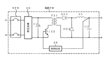
図5は、本発明の第4の実施の形態を説明するための回路図である。第4の実施の形態は、電源内部の整流平滑部に本発明を適用したものである。この実施の形態は、請求項7〜10に対応する。
【0049】
すなわち、電源PWは、図5に示すように、ノン・ヒューズ・ブレーカNFBと、整流回路20と、平滑用コンデンサC2と、トランスT21と、スイッチングトランジスタTr22と、ダイオードD23,D24と、コイル25と、平滑用コンデンサC3と、制御回路26とから構成されている。
交流電流は、ノン・ヒューズ・ブレーカNFBを介して、整流回路20と平滑用コンデンサC2に入力されて、直流に変換される。得られた直流はスイッチングトランジスタTr22によりオン/オフされ、トランスT21の一次側に入力される。トランスT22の二次側では、ダイオードD23,D24により整流され、コイル25とコンデンサ23により平滑され、直流として出力される。制御回路26は電源の出力電圧を検出し、出力電圧があらかじめ定められた電圧になるように、例えばPWM制御により、スイッチングトランジスタTr22をオン/オフ制御するものである。
【0050】
この第4の実施の形態は、図5に示す平滑用コンデンサC2の蓄積電荷を急速に放電させるとき、図1〜図4に示す各実施の形態で示す回路を、各実施の形態と同様の手法により、適用することができるというものである。
したがって、第4の実施の形態によれば、電源内部の整流平滑部に設けられた平滑用コンデンサの蓄積電荷を急速に放電することができる。したがって、作業者が感電する事故を防止することが可能になる。また、電源内部の部品発熱及び内部損失を低減することが可能になる。
【0051】
図7は、本発明の第5の実施の形態を説明するための回路図である。図7(a)に示すように、前記第1〜第4の実施の形態においては、電力を消費するための抵抗R1とFETQ1の直列回路を用いて、AC/DC変換部に設けられた平滑用コンデンサ(例えば、図1のコンデンサC参照)に蓄積されている電荷を強制的に放電させた。
【0052】
しかし、図7(a)に示す抵抗R1における電力消費が大きいと、抵抗R1とFETQ1の回路から構成される放電回路が溶断する可能性が生じる。
そこで、第5の実施の形態においては、抵抗(R1)による電力消費を小さくして、主にFETQ1において電力消費を行うように工夫している。
ここで、第5の実施の形態においては、FETQ1と抵抗R6の直列回路が放電回路である。また、この実施の形態は請求項11に対応している。
【0053】
以下、第5の実施の形態の動作を説明する。
図7(b)に示すように、内部エラー検出信号又は運転停止状態を示すドライブ信号等がスイッチングIC14に入力されると、スイッチングIC14が起動して、それまでオフ状態にあったFETQ1にオン/オフ動作を開始させる。
ここで、スイッチングIC14には、平滑用コンデンサの+電圧が抵抗R7を介して印加され、かつ前記印加電圧はツェナーダイオードZD3により一定電圧に保持されている。したがって、スイッチングIC14は、前記一定電圧により安定して動作するように構成されている。
【0054】
スイッチングIC14は、前記内部エラー検出信号又はドライブ信号等を受けて、FETQ1のオン/オフ制御を次のように行う。
すなわち、FETQ1のゲートにプラス電圧が印加されるタイミングでは、FETQ1がオンして、FETQ1と抵抗R6を介して平滑用コンデンサに蓄積された電荷を放電する。逆に、FETQ1のゲートにグランド電位が印加されるタイミングでは、FETQ1がオフして、前記平滑用コンデンサに蓄積された電荷の放電を行わない。
【0055】
ここで、オペアンプOP1の+入力端子には前記抵抗R6のFETQ1側の電圧が印加され、かつオペアンプOP1の−入力端子はツェナーダイオードZD4を介してグランドに接続されている。したがって、スイッチングIC4は、オペアンプOP1を介して、抵抗R6のFETQ1側の電圧が一定になるように、FETQ1をオン/オフ制御する。換言すれば、スイッチングIC4は、FETQ1に流れる電流が過大にならないようにリニア制御し、オン幅を制御している。
【0056】
請求項11との対応関係は、次のとおりである。すなわち、スイッチング素子と抵抗の直列回路は、FETQ1と抵抗R6の直列回路が対応する。また、スイッチング素子をオン/オフ制御する制御手段は、スイッチングIC14とオペアンプOP1とツェナーダイオードZD3、ZD4等が対応する。また、AC/DC変換部から運転停止を示す信号は、内部エラー信号やドライブ信号が対応する。
【0057】
この実施の形態によれば、抵抗R6の値は小さく設定可能である。そして、電力消費は、主にFETQ1において行われる。具体的には、抵抗R6は、大電力型の抵抗ではなく、消費電力が数ワット程度の抵抗を用いている。
したがって、第5の実施の形態によれば、AC/DC変換部に設けられている平滑用コンデンサに蓄積されている電荷を強制的に放電させることを可能にするとともに、放電に起因して、前記FETQ1と抵抗R6とから成る放電回路が溶断する事態を防止することができる。
【0058】
さらに、平滑用コンデンサCの容量が大きく、放電電荷量が多い場合には、FETQ1の代わりに大電流を流すことができるパワーリレーやIGBTなどの接点を用いればよい。
【0059】
【発明の効果】
本発明によれば、電源ラックのメインテナンス時等に、作業者が感電事故を起こすのを防止することが可能になる。
【0060】
本発明によれば、電源ラックの運転時に、パワー・ディストリビューション・ユニットやパワー・モジュールにおける部品発熱及び内部損失を低減することが可能になる。
本発明によれば、電源内部の整流平滑部においても、メインテナンス時等に電源内部の整流平滑部に設けられた平滑用コンデンサの蓄積電荷を急速に放電することが可能になる。また、電源内部の整流平滑部においても、部品発熱及び内部損失を低減することが可能になる。
【図面の簡単な説明】
【図1】本発明の第1の実施の形態を示す回路図である。
【図2】第1の実施の形態の変形例を示す回路図である。
【図3】本発明の第2の実施の形態を示す回路図である。
【図4】本発明の第3の実施の形態を示す説明図である。
【図5】本発明の第4の実施の形態を説明するための回路図である。
【図6】整流平滑回路の種類を示す回路図である。
【図7】本発明の第5の実施の形態を説明するための回路図である。
【図8】従来の電源ラックの回路図である。
【図9】電源ラックを示す斜視図である。
【符号の説明】
C,C2,C3 平滑用コンデンサ
D23,D24 ダイオード
NFB ノン・ヒューズ・ブレーカ
OP,OP1 オペアンプ
PDU パワー・ディストリビューション・ユニット
PWR BP パワーサプライ・バックプレイン
PM,PMa〜PMn パワー・モジュール
P パターン
PW 電源
Q1 FET
R,R1,R2,R4,R5,R6,R7 抵抗
SW1,SW2 スイッチ
T,T21 トランス
Tr,Tr22 スイッチングトランジスタ
ZD1,ZD2,ZD3,ZD4 ツェナーダイオード
1 交流電源
2 整流回路
3 エラー検出回路
4 スイッチングトランジスタ
5 フォトカプラ
14 スイッチングIC
20 整流回路
25 コイル
26 制御回路[0001]
TECHNICAL FIELD OF THE INVENTION
The present invention is intended to prevent an electric shock accident of a worker at the time of maintenance of the DC / DC conversion unit or the like in a power supply rack configured by unitizing an AC / DC conversion unit and a plurality of DC / DC conversion units. A preferred power supply rack and a power supply.
[0002]
[Prior art]
FIG. 8 is a circuit diagram of a conventional power supply rack configured by unitizing a power distribution unit PDU (AC / DC converter) and a plurality of power modules PMa to PMn (DC / DC converter). . FIG. 9 is a perspective view showing the power supply rack shown in FIG. In the following description, the AC / DC converter described in the technical field to which the invention pertains is referred to as a power distribution unit PDU, and the DC / DC converter is referred to as a power module PM.
[0003]
As is clear from FIGS. 8 and 9, the power distribution unit PDU and the plurality of power modules PMa to PMn are configured to be detachable from the power supply backplane PWR BP (Power Supply Buck Plane). Have been.
The power distribution unit PDU rectifies the AC current output from the
[0004]
The power supply backplane PWR BP includes a plurality of power modules PMa, PMb to PMn. Each of the power modules PMa to PMn converts a DC voltage received from the power supply / backplane PWR BP into a predetermined voltage and supplies it to each load (not shown). Here, when the DC voltage supplied from the power distribution unit PDU is high, the power modules PMa to PMn usually use an insulated DC / DC converter.
[0005]
[Patent Document 1]
JP-A-9-283189 (page 2)
[0006]
[Problems to be solved by the invention]
The power rack shown in FIG. 8 has the following problems.
[0007]
When the operator performs maintenance on the power supply rack shown in FIG. 8, it is necessary to prevent an electric shock accident caused by the electric charge accumulated in the smoothing capacitor C in the power distribution unit PDU.
When the power distribution unit PDU is turned off, the electric charge stored in the smoothing capacitor C is discharged through the resistor R, thereby preventing an electric shock accident of the worker.
[0008]
However, the discharge through the resistor R is difficult to discharge in a short time due to a problem of heat generation and a problem of a mounting space. Therefore, there is a risk that the worker may mistakenly think that the discharge has ended, and may suffer an electric shock accident.
In addition, since current flows through the resistor R at all times during operation of the power supply rack, it directly leads to the problem of heat generation of parts and the problem of internal loss during operation of the power distribution unit PDU.
[0009]
In addition, the problem of component heat generation and the problem of internal loss also become a problem in a power module that operates by receiving power from a power distribution unit PDU.
[0010]
SUMMARY OF THE INVENTION The present invention has been made in view of the above-described problems of the related art, and enables, for example, at the time of maintenance of a power supply rack, to rapidly discharge the accumulated charge of a smoothing capacitor, thereby causing an electric shock accident to a worker. It is an object of the present invention to provide a power supply rack suitable for preventing the power supply from being damaged.
Another object of the present invention is to provide a power supply rack suitable for reducing heat generation and internal loss of components in a power distribution unit and a power module during operation of the power supply rack.
[0011]
Another object of the present invention is to provide a power supply which is capable of rapidly discharging the accumulated charge of a smoothing capacitor provided in a rectifying / smoothing section inside a power supply and which is suitable for preventing an operator from an electric shock accident. Is to provide.
Another object of the present invention is to provide a power supply capable of reducing heat generation and internal loss of components.
[0012]
[Means for Solving the Problems]
The power supply rack according to
[0013]
The power supply rack according to
[0014]
The power supply rack according to
5. The power supply rack according to claim 4, wherein the AC / DC conversion unit and a plurality of DC / DC conversion units are unitized, and the drive signal indicating a normal operation state or an operation stop state from the AC / DC conversion unit. Is output, the switch is set to a first state when the drive signal indicates a normal operation state, and a switch is set to a second state when the drive signal indicates an operation stop state; And a discharge circuit for discharging the electric charge stored in the smoothing capacitor provided in the AC / DC converter when the state is set to the state described above.
[0015]
The power supply rack according to
[0016]
A power supply rack according to claim 6 is the power supply rack according to any one of
The power supply according to
[0017]
The power supply according to claim 8 is a power supply including an AC / DC conversion unit, and discharges electric charges accumulated in a smoothing capacitor present in a smoothing rectification unit provided in the AC / DC conversion unit. A switch and a discharge circuit according to any one of the third aspects are provided.
The power supply according to claim 9 is a power supply including an AC / DC conversion unit, and discharges electric charges accumulated in a smoothing capacitor present in a smoothing rectification unit provided in the AC / DC conversion unit. , A switch open circuit and a discharge circuit.
[0018]
According to a tenth aspect of the present invention, in the power supply having an AC / DC converter, the electric charge accumulated in a smoothing capacitor present in a smoothing rectifier provided in the AC / DC converter is discharged. A switch, a switch open circuit, and a discharge circuit are provided.
The power supply according to claim 11, further comprising: a switching element configured to discharge an electric charge accumulated in a smoothing capacitor existing in a smoothing rectification unit provided in the AC / DC conversion unit. Operates when a signal indicating operation stop is output from the series circuit and the AC / DC converter, detects a voltage between the resistor and the switching element, and adjusts the detected voltage to a predetermined value. And control means for controlling on / off of the switching element.
[0019]
According to the power supply rack of the first to third aspects, the electric charge accumulated in the smoothing capacitor can be forcibly discharged by the operation of the auxiliary switch and the discharge circuit.
According to the power supply rack of the fourth aspect, the charge accumulated in the smoothing capacitor present in the AC / DC converter can be forcibly discharged by the operation of the switch and the discharge circuit.
[0020]
According to the power supply rack of the fifth aspect, the electric charge accumulated in the smoothing capacitor existing in the smoothing rectifier can be forcibly discharged by the function of the switch, the switch open circuit, and the discharge circuit.
[0021]
According to the power supply rack according to the sixth aspect, the charge accumulated in the smoothing capacitor existing in the smoothing rectifier can be forcibly discharged by the function of the switch and the discharge circuit.
According to the power supply of the seventh aspect, the electric charge accumulated in the smoothing capacitor present in the smoothing rectifier can be forcibly discharged by the operation of the auxiliary switch and the discharge circuit.
[0022]
According to the power supply according to the eighth aspect, the charge accumulated in the smoothing capacitor existing in the smoothing rectifier can be forcibly discharged by the function of the switch and the discharge circuit.
According to the power supply of the ninth aspect, the charge accumulated in the smoothing capacitor existing in the smoothing rectification unit can be forcibly discharged by the operation of the switch, the switch open circuit, and the discharge circuit.
[0023]
According to the power supply of the tenth aspect, the charge accumulated in the smoothing capacitor existing in the smoothing rectification unit is forcibly discharged by the function of the switch, the switch open circuit, the switch open circuit, and the discharge circuit. Can be.
According to the power supply of claim 11, since the current flowing in the series circuit can be linearly controlled, power consumption is mainly performed in the switching elements in the series circuit, and power consumption due to the resistance in the series circuit is reduced. Can be smaller. Therefore, it is possible to forcibly discharge the electric charge stored in the smoothing capacitor provided in the AC / DC converter, and the discharge circuit including the series circuit of the resistor and the switching element is blown. Can be prevented.
[0024]
BEST MODE FOR CARRYING OUT THE INVENTION
Hereinafter, embodiments of the present invention will be described.
FIG. 1 is a circuit diagram showing a first embodiment of the present invention. In FIG. 1, the same parts as those of the related art are denoted by the same reference numerals, and description thereof will be omitted. Note that the first embodiment corresponds to
[0025]
The first embodiment shown in FIG. 1 is different from the prior art shown in FIG. 8 in that a circuit comprising resistors R1 and R2, an FET Q1, a Zener diode ZD1 and a switch SW1 is provided on the + side of a smoothing capacitor C. It is that you are. Here, the switch SW1 is an auxiliary switch of the non-fuse breaker NFB, and is a switch that is turned off in synchronization with the non-fuse breaker NFB being cut off. Further, the discharge resistor R provided in the prior art shown in FIG. 8 is not provided. The resistor R1 corresponds to the resistor R. Further, the resistor R2 has a sufficiently large resistance value.
[0026]
Hereinafter, the operation of the first embodiment shown in FIG. 1 will be described.
During normal operation, the switch SW1 is on because the non-fuse breaker NFB is in a conductive state. Therefore, the ground potential is applied to the gate of the FET Q1 through the switch SW1, and the FET Q1 maintains the off state. At this time, the accumulated charge of the smoothing capacitor C is not discharged through the switch SW1 because the resistor R2 has a sufficiently large resistance value.
[0027]
When the worker shuts off the non-fuse breaker NFB for maintenance, the switch SW1 is turned off in conjunction with it. As a result, the gate potential of the FET Q1 changes from the ground potential to the Zener voltage of the Zener diode ZD1, and the FET Q1 turns on. Therefore, the electric charge stored in the smoothing capacitor C is discharged to the ground through the resistor R1 → FETQ1. At this time, the resistor R1 serves as a discharge resistor.
[0028]
Note that the resistor R2 is provided to allow a minute current to flow through the resistor R2 and the switch SW1 when the switch SW1 is on. It is also provided to generate the Zener voltage when the switch SW1 is off.
[0029]
According to the first embodiment, when the operator performs maintenance, the FET Q1 is turned on by discharging the non-fuse breaker NFB, and the accumulated charge in the smoothing capacitor C can be discharged. Therefore, it is possible to prevent an accident in which the worker receives an electric shock. Further, it is possible to reduce heat generation and internal loss of components in the power distribution unit and the power module.
[0030]
Note that a relay, a transistor, an IGBT, or the like can be used instead of the FET Q1.
Further, when the capacity of the smoothing capacitor C is large and the amount of discharged electric charge is large, a contact such as a power relay through which a large current can flow may be used instead of the FET Q1. This corresponds to claim 6.
[0031]
In the above-described first embodiment, the FET Q1 is turned on with the non-fuse breaker NFB turned off, but the present embodiment is not limited to this.
For example, when the AC input to the power distribution unit PDU is cut off, the power distribution unit PDU outputs a power failure detection signal. Using the power failure detection signal, the switch SW1 may be turned off, the FET Q1 may be turned on, and the accumulated charge in the smoothing capacitor C may be discharged.
[0032]
Further, the switch SW1 may be turned off, the FET Q1 may be turned on, and the charge stored in the capacitor C may be discharged using an internal error signal output when the non-fuse breaker NFB, the
FIG. 2 is a circuit diagram showing a modification of the first embodiment using the above-described internal error signal. That is, the
[0033]
FIG. 3 is a circuit diagram showing a second embodiment of the present invention. The second embodiment is an embodiment in which a power distribution unit PDU is operated by PWM control. In FIG. 3, the same parts as those in the related art are denoted by the same reference numerals, and description thereof will be omitted. This embodiment corresponds to claim 4.
As shown in FIG. 3, the DC is converted to DC by the
[0034]
The + side of the smoothing capacitor C has the configuration of the resistors R1, R2, the FET Q1, and the Zener diode ZD1 as in FIG. The gate of the FET Q1 is connected to the collector of the phototransistor of the
[0035]
On the other hand, the light emitting diode of the
[0036]
Here, the drive signal shown in FIG. 3 is output from the power distribution unit PDU, becomes H when the power distribution unit PDU is performing the normal operation by the PWM control, and becomes the power distribution unit PDU. Is a signal that becomes L when stopped by the PWM control. The switch SW2 receives the drive signal and turns off when the drive signal is H (normal operation) and turns on when the drive signal is L (stop operation).
[0037]
Next, the operation of the second embodiment shown in FIG. 3 will be described.
During a normal operation, the AC current output from the
[0038]
On the one hand, the DC output on the secondary side is input to a power module PM via a power supply backplane PWR BP (see FIG. 1). On the other hand, the DC output is input to a circuit comprising resistors R1, R2, FET Q1, zener diode ZD1, and
At this time, the switch SW2 is turned off in response to the drive signal (H state). Therefore, the output current of the internal auxiliary power supply flows through the light emitting diode in the
[0039]
Next, an operation at the time of maintenance of a worker and an operation at the time of an accident will be described.
For example, it is assumed that an operator turns off the
[0040]
When the switching transistor Tr is turned off, no current flows to the primary side of the transformer T, so that no current flows to the secondary side of the transformer T. Therefore, charging of the smoothing capacitor C is stopped.
At the same time, the voltage of the internal auxiliary power supply is grounded via the resistor R5 and the switch SW2. As a result, no current flows through the photodiode in the
[0041]
According to the second embodiment, when the operator performs maintenance or when an accident occurs, the electric charge accumulated in the smoothing capacitor C can be immediately discharged. Therefore, it is possible to prevent an accident in which the worker receives an electric shock. Further, it is possible to reduce heat generation and internal loss of components in the power distribution unit and the power module.
[0042]
Note that a relay, a transistor, an IGBT, or the like can be used instead of the FET Q1.
Further, when the capacity of the smoothing capacitor C is large and the amount of discharge charge is large, a contact such as a power relay capable of flowing a large current may be used instead of the FET Q1. This corresponds to claim 6.
[0043]
Further, as the drive signal, the power failure detection signal, the error signal, or the like may be used.
FIG. 4 is a diagram showing a third embodiment of the present invention. In the third embodiment, when the operator pulls out the power distribution unit PDU from the power supply backplane PWR BP, the smoothing capacitor is rapidly discharged. In FIG. 4, the same parts as those in the related art are denoted by the same reference numerals, and description thereof will be omitted. This embodiment corresponds to claim 5.
[0044]
As shown in FIGS. 4A and 4B, a pattern P is provided in the power supply backplane PWR BP. 4A, the first terminal of the pattern P is connected to the gate of the FET Q1 in the power distribution unit PDU, and the second terminal of the pattern P is connected to the power distribution unit PDU. Grounded within.
[0045]
Here, the FET Q1 in the power distribution unit PDU corresponds to, for example, the FET Q1 (see FIG. 1) in the first embodiment. Similarly, the ground shown in the power distribution unit PDU corresponds to, for example, the ground to which the switch SW1 (see FIG. 1) in the first embodiment is connected. The pattern P provided on the power supply backplane PWR BP corresponds to, for example, the switch SW1 (see FIG. 1) in the first embodiment.
[0046]
When the operator pulls out the power distribution unit PDU, a Zener voltage is applied to the gate of the FET Q1 that has been short-circuited by the pattern P, and the FET Q1 turns on. Thereby, the electric charge accumulated in the smoothing capacitor C (see FIG. 1) is discharged.
According to the third embodiment, when the operator performs maintenance, the charge accumulated in the smoothing capacitor C can be discharged by pulling out the power distribution unit PDU. Therefore, it is possible to prevent an accident in which the worker receives an electric shock. Further, it is possible to reduce heat generation and internal loss of components in the power distribution unit and the power module.
[0047]
Note that a relay, a transistor, an IGBT, or the like can be used instead of the FET Q1.
Further, when the capacity of the smoothing capacitor C is large and the amount of discharge charge is large, a contact such as a power relay capable of flowing a large current may be used instead of the FET Q1. This corresponds to claim 6.
[0048]
In the first to third embodiments described above, the rectifying / smoothing circuit used for the rectifying / smoothing unit of the power distribution unit is a peak rectifying type shown in FIG. 6A, and FIG. And the insulation type (PWM control) shown in FIGS. 6C and 6D. Since these circuits are known, the description of the operation is omitted. Here, it should be noted that the invention according to
FIG. 5 is a circuit diagram for explaining a fourth embodiment of the present invention. In the fourth embodiment, the present invention is applied to a rectifying and smoothing unit inside a power supply. This embodiment corresponds to
[0049]
That is, as shown in FIG. 5, the power supply PW includes a non-fuse breaker NFB, a
The AC current is input to the
[0050]
In the fourth embodiment, when the accumulated charge of the smoothing capacitor C2 shown in FIG. 5 is rapidly discharged, the circuits shown in the respective embodiments shown in FIGS. It can be applied by a method.
Therefore, according to the fourth embodiment, it is possible to rapidly discharge the charge accumulated in the smoothing capacitor provided in the rectifying / smoothing section inside the power supply. Therefore, it is possible to prevent an accident in which the worker receives an electric shock. Further, it is possible to reduce heat generation and internal loss of components inside the power supply.
[0051]
FIG. 7 is a circuit diagram for explaining a fifth embodiment of the present invention. As shown in FIG. 7A, in the first to fourth embodiments, a smoothing circuit provided in an AC / DC converter is provided by using a series circuit of a resistor R1 for consuming power and an FET Q1. The electric charge accumulated in the capacitor for use (for example, see the capacitor C in FIG. 1) was forcibly discharged.
[0052]
However, if the power consumption of the resistor R1 shown in FIG. 7A is large, there is a possibility that the discharge circuit including the circuit of the resistor R1 and the FET Q1 is blown.
Therefore, in the fifth embodiment, the power consumption due to the resistor (R1) is reduced so that power consumption is mainly performed in the FET Q1.
Here, in the fifth embodiment, a series circuit of the FET Q1 and the resistor R6 is a discharge circuit. This embodiment corresponds to claim 11.
[0053]
Hereinafter, the operation of the fifth embodiment will be described.
As shown in FIG. 7B, when an internal error detection signal or a drive signal indicating an operation stop state is input to the switching
Here, the positive voltage of the smoothing capacitor is applied to the switching
[0054]
The switching
That is, at the timing when the plus voltage is applied to the gate of the FET Q1, the FET Q1 turns on and discharges the electric charge accumulated in the smoothing capacitor via the FET Q1 and the resistor R6. Conversely, at the timing when the ground potential is applied to the gate of the FET Q1, the FET Q1 is turned off and the electric charge accumulated in the smoothing capacitor is not discharged.
[0055]
Here, the voltage on the FET Q1 side of the resistor R6 is applied to the + input terminal of the operational amplifier OP1, and the-input terminal of the operational amplifier OP1 is connected to the ground via the Zener diode ZD4. Therefore, the switching IC 4 controls on / off of the FET Q1 via the operational amplifier OP1 such that the voltage of the resistor R6 on the FET Q1 side becomes constant. In other words, the switching IC 4 performs linear control so that the current flowing through the FET Q1 does not become excessive, and controls the ON width.
[0056]
The correspondence with claim 11 is as follows. That is, the series circuit of the switching element and the resistor corresponds to the series circuit of the FET Q1 and the resistor R6. Further, the control means for controlling on / off of the switching element corresponds to the switching
[0057]
According to this embodiment, the value of the resistor R6 can be set small. The power consumption is mainly performed in the FET Q1. Specifically, the resistor R6 is not a large power type resistor but a resistor whose power consumption is about several watts.
Therefore, according to the fifth embodiment, it is possible to forcibly discharge the charge stored in the smoothing capacitor provided in the AC / DC converter, It is possible to prevent the discharge circuit including the FET Q1 and the resistor R6 from being blown.
[0058]
Further, when the capacity of the smoothing capacitor C is large and the amount of discharge charge is large, a contact such as a power relay or an IGBT capable of flowing a large current may be used instead of the FET Q1.
[0059]
【The invention's effect】
ADVANTAGE OF THE INVENTION According to this invention, it becomes possible to prevent a worker from causing an electric shock accident at the time of maintenance of a power supply rack etc.
[0060]
Advantageous Effects of Invention According to the present invention, it is possible to reduce heat generation and internal loss of components in a power distribution unit or a power module during operation of a power supply rack.
ADVANTAGE OF THE INVENTION According to this invention, also in the rectification | smoothing part in a power supply, it becomes possible at the time of a maintenance etc. to rapidly discharge the electric charge stored in the smoothing capacitor provided in the rectification and smoothing part in a power supply. In addition, heat generation and internal loss of components can be reduced in the rectifying and smoothing unit inside the power supply.
[Brief description of the drawings]
FIG. 1 is a circuit diagram showing a first embodiment of the present invention.
FIG. 2 is a circuit diagram showing a modification of the first embodiment.
FIG. 3 is a circuit diagram showing a second embodiment of the present invention.
FIG. 4 is an explanatory diagram showing a third embodiment of the present invention.
FIG. 5 is a circuit diagram for explaining a fourth embodiment of the present invention.
FIG. 6 is a circuit diagram showing types of rectifying and smoothing circuits.
FIG. 7 is a circuit diagram for explaining a fifth embodiment of the present invention.
FIG. 8 is a circuit diagram of a conventional power rack.
FIG. 9 is a perspective view showing a power supply rack.
[Explanation of symbols]
C, C2, C3 Smoothing capacitor
D23, D24 Diode
NFB non-fuse breaker
OP, OP1 Operational amplifier
PDU power distribution unit
PWR BP Power Supply Backplane
PM, PMa-PMn power module
P pattern
PW power supply
Q1 FET
R, R1, R2, R4, R5, R6, R7 Resistance
SW1, SW2 switch
T, T21 transformer
Tr, Tr22 switching transistor
ZD1, ZD2, ZD3, ZD4 Zener diode
1 AC power supply
2 Rectifier circuit
3 Error detection circuit
4 Switching transistor
5 Photo coupler
14 Switching IC
20 Rectifier circuit
25 coils
26 Control circuit
Claims (11)
前記AC/DC変換部に設けられ、前記AC/DC変換部に入力されているAC入力が遮断されたとき開閉動作を行う補助スイッチを有するノン・ヒューズ・ブレーカと、
ノン・ヒューズ・ブレーカの補助スイッチの開閉動作に応じて、AC/DC変換部に設けられた平滑用コンデンサに蓄積されている電荷を強制的に放電させる放電回路と
を備えたことを特徴とする電源ラック。In a power rack configured by unitizing an AC / DC converter and a plurality of DC / DC converters,
A non-fuse breaker provided in the AC / DC converter and having an auxiliary switch for performing an opening / closing operation when an AC input being input to the AC / DC converter is cut off;
A discharge circuit for forcibly discharging the electric charge stored in the smoothing capacitor provided in the AC / DC converter in accordance with the opening / closing operation of the auxiliary switch of the non-fuse breaker. Power rack.
前記補助スイッチの代わりに、前記AC/DC変換部が故障したとき、前記AC/DC変換部から出力される内部エラー信号によって開閉動作を行うスイッチを有することを特徴とする電源ラック。The power supply rack according to claim 1,
A power supply rack comprising a switch that performs an opening / closing operation in response to an internal error signal output from the AC / DC converter when the AC / DC converter fails, instead of the auxiliary switch.
前記補助スイッチの代わりに、前記AC/DC変換部に入力されているAC入力が遮断されたとき、前記AC/DC変換部から出力される停電検出信号によって開閉動作をするスイッチを有することを特徴とする電源ラック。The power supply rack according to claim 1,
A switch is provided in place of the auxiliary switch, the switch performing an open / close operation according to a power failure detection signal output from the AC / DC converter when the AC input to the AC / DC converter is cut off. And power rack.
前記AC/DC変換部から通常運転状態又は運転停止状態を示すドライブ信号が出力されたとき、前記ドライブ信号が通常運転状態を示すとき第1の状態に設定され、前記ドライブ信号が運転停止状態を示すとき第2の状態に設定されるスイッチと、
前記スイッチが第2の状態に設定されたとき、AC/DC変換部に設けられた平滑用コンデンサに蓄積されている電荷を放電させる放電回路と
を備えたことを特徴とする電源ラック。In a power rack configured by unitizing an AC / DC converter and a plurality of DC / DC converters,
When a drive signal indicating a normal operation state or an operation stop state is output from the AC / DC conversion unit, the drive signal is set to a first state when the drive signal indicates a normal operation state. A switch set to a second state when indicated,
A power supply rack comprising: a discharge circuit that discharges electric charges stored in a smoothing capacitor provided in an AC / DC converter when the switch is set to a second state.
前記AC/DC変換部と前記複数のDC/DC変換部を着脱可能な基板と、
前記基板から前記AC/DC変換部を引き抜くことにより、前記AC/DC変換部に設けられたスイッチを開動作させるスイッチ開回路と、
前記スイッチの開動作に応じて、前記AC/DC変換部に設けられた平滑用コンデンサに蓄積されている電荷を強制的に放電させる放電回路と
を備えたことを特徴とする電源ラック。In a power rack configured by unitizing an AC / DC converter and a plurality of DC / DC converters,
A substrate on which the AC / DC converter and the plurality of DC / DC converters are detachable;
A switch open circuit for pulling out the AC / DC converter from the substrate to open a switch provided in the AC / DC converter;
A power supply rack, comprising: a discharge circuit for forcibly discharging electric charges stored in a smoothing capacitor provided in the AC / DC converter in response to an opening operation of the switch.
前記放電回路は、前記スイッチとして大電流を流すことが可能なスイッチを有することを特徴とする電源ラック。The power supply rack according to any one of claims 1 to 5,
The power supply rack, wherein the discharge circuit includes a switch capable of flowing a large current as the switch.
AC/DC変換部内に設けられた平滑整流部に存在する平滑用コンデンサに蓄積された電荷を放電させる請求項1に記載の補助スイッチと放電回路を備えたことを特徴とする電源。In a power supply having an AC / DC conversion unit,
2. A power supply comprising the auxiliary switch and the discharge circuit according to claim 1, which discharges electric charges accumulated in a smoothing capacitor present in a smoothing rectifier provided in the AC / DC converter.
AC/DC変換部内に設けられた平滑整流部に存在する平滑用コンデンサに蓄積された電荷を放電させる請求項2乃至請求項3のいずれか一方に記載のスイッチと放電回路を備えたことを特徴とする電源。In a power supply having an AC / DC conversion unit,
4. A switch and a discharge circuit according to claim 2, wherein the switch and the discharge circuit discharge electric charges accumulated in a smoothing capacitor existing in a smoothing rectifier provided in the AC / DC converter. And power supply.
AC/DC変換部内に設けられた平滑整流部に存在する平滑用コンデンサに蓄積された電荷を放電させる請求項4に記載のスイッチと放電回路を備えたことを特徴とする電源。In a power supply having an AC / DC conversion unit,
5. A power supply comprising the switch and the discharge circuit according to claim 4, which discharges electric charges stored in a smoothing capacitor present in a smoothing rectifier provided in the AC / DC converter.
AC/DC変換部内に設けられた平滑整流部に存在する平滑用コンデンサに蓄積された電荷を放電させる請求項5に記載のスイッチとスイッチ開回路と放電回路を備えたことを特徴とする電源。In a power supply having an AC / DC conversion unit,
6. A power supply comprising: the switch, the switch open circuit, and a discharge circuit according to claim 5, which discharges electric charges accumulated in a smoothing capacitor existing in a smoothing rectifier provided in the AC / DC converter.
AC/DC変換部内に設けられた平滑整流部に存在する平滑用コンデンサに蓄積された電荷を放電させるスイッチング素子と抵抗の直列回路と、
AC/DC変換部から運転停止を示す信号が出力されたとき動作し、前記抵抗と前記スイッチング素子の間の電圧を検出して、検出された電圧が所定の値になるようにスイッチング素子をオン/オフ制御する制御手段と
を有していることを特徴とする電源。In a power supply having an AC / DC conversion unit,
A series circuit of a switching element and a resistor for discharging electric charges accumulated in a smoothing capacitor existing in a smoothing rectifier provided in an AC / DC converter;
It operates when a signal indicating operation stop is output from the AC / DC converter, detects a voltage between the resistor and the switching element, and turns on the switching element so that the detected voltage becomes a predetermined value. And a control unit for performing on / off control.
Priority Applications (1)
| Application Number | Priority Date | Filing Date | Title |
|---|---|---|---|
| JP2003071985A JP2004282921A (en) | 2003-03-17 | 2003-03-17 | Power supply rack and power supply |
Applications Claiming Priority (1)
| Application Number | Priority Date | Filing Date | Title |
|---|---|---|---|
| JP2003071985A JP2004282921A (en) | 2003-03-17 | 2003-03-17 | Power supply rack and power supply |
Publications (1)
| Publication Number | Publication Date |
|---|---|
| JP2004282921A true JP2004282921A (en) | 2004-10-07 |
Family
ID=33288291
Family Applications (1)
| Application Number | Title | Priority Date | Filing Date |
|---|---|---|---|
| JP2003071985A Pending JP2004282921A (en) | 2003-03-17 | 2003-03-17 | Power supply rack and power supply |
Country Status (1)
| Country | Link |
|---|---|
| JP (1) | JP2004282921A (en) |
Cited By (4)
| Publication number | Priority date | Publication date | Assignee | Title |
|---|---|---|---|---|
| JP2006121849A (en) * | 2004-10-22 | 2006-05-11 | Toyoda Mach Works Ltd | Dc stabilized power supply |
| JP2008220111A (en) * | 2007-03-07 | 2008-09-18 | Fujitsu Telecom Networks Ltd | Power supply unit equipped with power failure detecting circuit |
| WO2011026337A1 (en) * | 2009-09-01 | 2011-03-10 | 中兴通讯股份有限公司 | System and method for monitoring parallel base station power supply |
| CN112117911A (en) * | 2020-09-25 | 2020-12-22 | 江苏方天电力技术有限公司 | Converter device for converting Direct Current (DC) 750V into Direct Current (DC) 240V |
-
2003
- 2003-03-17 JP JP2003071985A patent/JP2004282921A/en active Pending
Cited By (5)
| Publication number | Priority date | Publication date | Assignee | Title |
|---|---|---|---|---|
| JP2006121849A (en) * | 2004-10-22 | 2006-05-11 | Toyoda Mach Works Ltd | Dc stabilized power supply |
| JP4626262B2 (en) * | 2004-10-22 | 2011-02-02 | 株式会社ジェイテクト | DC stabilized power supply |
| JP2008220111A (en) * | 2007-03-07 | 2008-09-18 | Fujitsu Telecom Networks Ltd | Power supply unit equipped with power failure detecting circuit |
| WO2011026337A1 (en) * | 2009-09-01 | 2011-03-10 | 中兴通讯股份有限公司 | System and method for monitoring parallel base station power supply |
| CN112117911A (en) * | 2020-09-25 | 2020-12-22 | 江苏方天电力技术有限公司 | Converter device for converting Direct Current (DC) 750V into Direct Current (DC) 240V |
Similar Documents
| Publication | Publication Date | Title |
|---|---|---|
| US10158282B1 (en) | Switching power supply device | |
| EP1178591B1 (en) | Power supply device with detection of malfunctioning | |
| US7339804B2 (en) | DC-DC converter | |
| US6088243A (en) | Power supply apparatus | |
| JP3557198B2 (en) | Switching power supply circuit and electronic equipment | |
| US20030169606A1 (en) | Start-up circuit for switched mode power supply | |
| JP4108457B2 (en) | Switching power supply | |
| US6023178A (en) | Pulse width control IC circuit and switching power supply unit | |
| JP2008048515A (en) | Switching power supply device | |
| JP4289904B2 (en) | AC-DC converter | |
| EP1118150A1 (en) | A resonant mode power supply having over-power and over-current protection | |
| US20040201937A1 (en) | Overcurrent protection circuit for switching power supply | |
| KR19990074214A (en) | Switched Mode Power Supplies with Low Voltage Protection Circuits | |
| JP2004282921A (en) | Power supply rack and power supply | |
| JP2020048372A (en) | DC power supply | |
| JP4030349B2 (en) | Power circuit | |
| JP2017005888A (en) | Switching power supply device | |
| JPH08149822A (en) | Switching regulator | |
| KR100226697B1 (en) | An over-load protection apparatus in a smps | |
| JP2003304684A (en) | Forward converter | |
| JP2002125368A (en) | Switching power supply and its control method | |
| JP2000078764A (en) | Non-contact feeding device | |
| KR200156513Y1 (en) | Apparatus for protecting a smps in a monitor | |
| JP2003125578A (en) | Switching power unit | |
| JP2010016962A (en) | Switching electric power unit |
Legal Events
| Date | Code | Title | Description |
|---|---|---|---|
| A621 | Written request for application examination |
Free format text: JAPANESE INTERMEDIATE CODE: A621 Effective date: 20050913 |
|
| A977 | Report on retrieval |
Free format text: JAPANESE INTERMEDIATE CODE: A971007 Effective date: 20090113 |
|
| A131 | Notification of reasons for refusal |
Free format text: JAPANESE INTERMEDIATE CODE: A131 Effective date: 20090121 |
|
| A521 | Written amendment |
Free format text: JAPANESE INTERMEDIATE CODE: A523 Effective date: 20090313 |
|
| A131 | Notification of reasons for refusal |
Free format text: JAPANESE INTERMEDIATE CODE: A131 Effective date: 20091006 |
|
| A02 | Decision of refusal |
Free format text: JAPANESE INTERMEDIATE CODE: A02 Effective date: 20100302 |