JP2004273055A - Information holding medium, and information recording method and system - Google Patents
Information holding medium, and information recording method and system Download PDFInfo
- Publication number
- JP2004273055A JP2004273055A JP2003064330A JP2003064330A JP2004273055A JP 2004273055 A JP2004273055 A JP 2004273055A JP 2003064330 A JP2003064330 A JP 2003064330A JP 2003064330 A JP2003064330 A JP 2003064330A JP 2004273055 A JP2004273055 A JP 2004273055A
- Authority
- JP
- Japan
- Prior art keywords
- layer
- information
- recording
- electrode
- storage medium
- Prior art date
- Legal status (The legal status is an assumption and is not a legal conclusion. Google has not performed a legal analysis and makes no representation as to the accuracy of the status listed.)
- Pending
Links
Images


Abstract
Description
【0001】
【発明の属する技術分野】
本発明は,光を用いて情報を記録,再生する情報保持媒体,情報記録方法,及び情報記録装置に関する。
【0002】
【従来の技術】
本願明細書中では,たとえば光ディスクのように,情報を記録・再生するための媒体を,情報保持媒体と称する。
【0003】
従来から、DVD−RAMのように、記録膜に相変化膜を用いるものや、CD−RやDVD−Rのように、有機材料を情報層とした光ディスクが存在している。有機材料を情報層とした光ディスクは,記録光源の波長に吸収を有する色素を含む情報層を有し,それに接する基板表面をレーザ照射で変質させて記録を行う。
【0004】
従来、例えば,特開昭63−122032号に記載されている通り、記録膜に電界を印加した状態でレーザ光を照射することによって,相変化記録膜に情報の記録を行う,電界効果型光ディスクが知られている。これは,上下の電極間にGeSbTe系などの相変化情報層をサンドイッチにした素子構造で使用される。記録膜に電界がかかることにより,レーザ光照射だけよりも相変化(結晶化)が促進されることを狙ったものである。
【0005】
また、特開平5−101454号には、光インタカレーション効果あるいは光デインタカレーション効果を示すWO3からなる半導体膜と、電解質膜とを接して配置し、光が照射されると電解質膜のイオンが光半導体に取り込まれて透明に変化する光情報記録媒体が記載されている。
【特許文献1】特開昭63−122032号
【特許文献2】特開平5−101454号
【発明が解決しようとする課題】
しかし、上記の特開平5−101454号では、電解質膜として、固体電解質と比較して応答速度が大きい液体電解質を用いている。しかしながら,本発明者らの検討の結果、セルの透過光強度が入射光強度の70%になるまでに要する時間が,少なくとも数十秒かかり,非常に遅いという課題があった。
【0006】
本発明の目的は,高速な光情報記録方法,情報保持媒体および装置を提供することにある。
【0007】
【課題を解決するための手段】
上記の問題点を解決するための本発明の構成を以下に述べる。
【0008】
本発明の情報保持媒体は,図1の断面構造に示すような構成を基本単位とする。基本単位は,導電性高分子エレクトロクロミック材料を含む情報層1と,情報層1に隣接して設けられた,電圧印加によって情報層1へ拡散するイオンを有する電解質層2と,情報層1および電解質層2の両側を,第1の電極3および第2の電極4によって挟んだ構造を有する。電極3,4は、電源5によって電圧が印加される。
【0009】
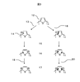
ここで,導電性高分子エレクトロクロミック材料とは,半導体的な導電性を有する高分子であり,かつ,電圧の印加により可逆的に色(吸収スペクトル)が変化する材料である。導電性高分子エレクトロクロミック材料としては,共役二重結合または三重結合でつながった共役系高分子であるポリアセチレン,ポリアニリン,ポリピロール,ポリチオフェン,およびそれらの誘導体が挙げられる。これらの導電性高分子エレクトロクロミック材料のエレクトロクロミズムは以下のような原理による。ここで,ポリチオフェンを例として説明する。図2はポリチオフェンの基底状態における電子共鳴構造を表したものであり,アロマティック型構造8とキノイド型構造9の2つの構造が可能である。アロマティック型構造8とキノイド型構造9では,アロマティック型構造8の方がエネルギーが低く,両者はエネルギー的に等価でないので,ポリチオフェンの基底状態は縮退していない。ポリチオフェン以外のポリアニリン,ポリピロール,ポリチオフェン,ポリフェニレンビニレンなども,同様に基底状態が縮退していない,非縮退系導電性高分子である。非縮退系導電性高分子のエレクトロクロミズムは,以下のようなポーラロン,バイポーラロンによって説明されることが,J. C. StreetらによるPhysical Review B,第28巻,No. 4,p. 2140−2145に記されている。図3は,ポリチオフェンのドーピングに伴う分子構造の変化を表したものである。ポリチオフェンの中性状態12にアクセプタをドープすると,まず1電子酸化13がおこり,1電子酸化状態14となる。ここで,ドーピングに用いるアクセプタとしては,Br2,I2,Cl2などのハロゲン類,BF3,PF5,AsF5,SbF5,SO3,BF4 ―,PF6 ―,AsF6 ―,SbF6 ―などのルイス酸,HNO3,HCl,H2SO4,HClO4,HF,CF3SO3Hなどのプロトン酸,FeCl3,MoCl3,WCl5などの遷移金属ハロゲン化物,テトラシアノエチレン(TCNE),7,7,8,8−テトラシアノキノジメタン(TCNQ)などの有機物質が挙げられる。1電子酸化状態14は,緩和過程15を経て正に荷電したポーラロン状態16となる。ポーラロンとは,理化学辞典第5版(1998年,岩波書店)によれば,結晶中の伝導電子がそのまわりの結晶格子の変形を伴って運動している状態をいう。ここでのポーラロン状態では,“結晶”を“ポリチオフェン分子の中性状態”と置き換え,“結晶格子の変形”を,“1電子酸化によるポリチオフェン分子の部分的なキノイド構造の出現”と考える。ポーラロン状態16のポリチオフェンにさらにアクセプタをドープすると,さらに酸化が進み,正の,バイポーラロン状態17となる。一方,ドナードーピングによっても,還元反応18により,負に荷電したポーラロン,バイポーラロンが生成する。ここで,ドーピングに用いるドナーとしては,Li,Na,K,Csのようなアルカリ金属,テトラエチルアンモニウム,テトラブチルアンモニウムなどの4級アンモニウムイオンが挙げられる。ポーラロンとバイポーラロンはともに,高分子鎖の上を移動するので,電流に寄与する。上記のドーパントのほかに,ポリマードーパントとよばれる高分子電解質を用いることも可能である。たとえば,ポリスチレンスルホン酸,ポリビニルスルホン酸,スルホン化ポリブタジエンがある。これらの高分子電解質の存在下,ポリアニリン,ポリチオフェン,ポリピロールを重合すると,生成する導電性高分子は用いた高分子電解質とのイオン複合体として得られる。ポリマードーパントの使用により,溶剤に不溶な導電性高分子を可溶化できるなど,加工性の改善に有効である。
【0010】
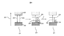
ポーラロンおよびバイポーラロンとエレクトロクロミズムとの関係は,非縮退系導電性高分子の電子状態をバンド構造によって表した,図4によって説明される。ここでは,アクセプタドーピングに伴う電子状態の変化を示す。ドーピングを行なっていない中性状態のバンド構造21では,価電子帯22の頂上のエネルギーと伝導帯23の底のエネルギーとの差として,禁制帯幅24と呼ばれる電子のエネルギー25の差が存在し,許容遷移26として,禁制帯幅24に対応したエネルギーの光が吸収される。吸収される光の波長が可視光の波長域にあるときには,着色して見える。ここで,非縮退系導電性高分子の禁制帯幅24は,一般的に無機半導体と同様に,0.1 eVから3 eVである。アクセプタドーピングの結果生成した正のポーラロン状態におけるバンド構造27では,価電子帯22と伝導帯23との間に,ポーラロン準位P+28およびポーラロン準位P−29の2つのポーラロン準位が生成する。ポーラロン状態における許容遷移30は,中性状態における許容遷移26と比較して,遷移エネルギー幅および遷移確率の点で異なることから,光の吸収特性が変化し,可視光域での変化は色の変化として観測される。さらにドーピングが進んだバイポーラロン状態におけるバンド構造31では,価電子帯22と伝導帯23との間に,新たにバイポーラロン準位BP+32およびバイポーラロン準位BP−33の2つのバイポーラロン準位が生成し,バイポーラロン状態における許容遷移34がさらに変化することから,光吸収特性もさらに変化する。非縮退系導電性高分子のドナードーピングによっても,同様に,ポーラロン準位およびバイポーラロン準位の生成に伴うバンド構造の変化に起因する許容遷移挙動の変化がエレクトロクロミズムとして観測される。
【0011】
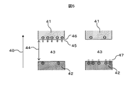
非縮退系導電性高分子のバンド構造は,シリコン系材料に代表される無機半導体のバンド構造とは全く異なるものである。図5は,無機半導体結晶における格子定数近傍における電子状態をバンド構造によって表したものであり,図の上の方が電子のエネルギー40が高いことを示す。伝導帯41の下端と価電子帯42の上端の間が禁制帯43であり,それらのエネルギー差が禁制帯幅44である。
【0012】
たとえば,シリコンの結晶にV族原子であるP,As,SbをドープしたN型半導体では,V族原子の最外殻の1個の電子が伝導帯41のすぐ下のドナー準位45に位置する。伝導帯の底46とドナー準位45のエネルギー差が小さいため,ドナー準位45にある電子が伝導帯41に容易に移って,電子に電界がかかるとプラス電位側に動き,電流が観測される。
【0013】
一方,シリコンの結晶にIII族原子であるホウ素(B)をドープしたP型半導体では,ホウ素原子がシリコン原子と置き換わり,価電子帯42の少し上のエネルギー準位にアクセプタ準位47ができる。価電子帯42に存在する電子は容易にアクセプタ準位に捕われ,価電子帯42の電子が抜けた跡である正孔が価電子帯42内を自由に動き,電流として観測される。
【0014】
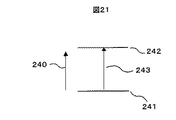
また,代表的な無機エレクトロクロミック材料で,無機半導体の性質を有する酸化タングステンは,電圧印加による,水素イオンあるいはリチウムイオンのようなアルカリ金属イオンの結晶格子中へのインターカレーションに伴い,無色(または淡黄色)から濃い青色に可逆的に変化する。このような酸化タングステンのエレクトロクロミズムは,6価のタングステン原子が,部分的に5価に還元された,混合原子価状態における原子価間遷移吸収によるものであり,図21を用いて説明できる。240は電子のエネルギーを示す。酸化タングステンの伝導帯はタングステン原子の5d軌道により構成される。混合原子価状態では,タングステン原子(5価)のエネルギー準位241からタングステン原子(6価)のエネルギー準位242への原子価間遷移243が起こり,この遷移が着色をもたらす。酸化モリブデン,酸化イリジウム,二酸化マンガン,酸化ニッケル,プルシアンブルー(2価と3価の混合原子価状態の鉄シアノ錯体)などのエレクトロクロミズムも同様の原理による。このように,無機エレクトロクロミック材料のエレクトロクロミズムは,結晶格子内へのイオンのインターカレーションによるので,着色速度,消色速度はともに遅く,着色状態と消色状態との切り替えには1分以上を要する。
【0015】
非縮退系導電性高分子のドーピングに伴うエレクトロクロミック特性を記録に利用するので,ここでは特に,エレクトロクロミズムを示す非縮退系導電性高分子を“導電性高分子エレクトロクロミック材料”と称する。
【0016】
なお、発明完成後に公知例調査を行った結果、特開平11−185288号と特開2002−184056号が見つかった。
【0017】
特開平11−185288号には、エレクトロクロミック層を有する媒体が記載されている。このエレクトロクロミック層は、電気化学反応を起こす物質による着色層と電気化学反応を媒介する電解質による電解質層からなる。そして、照射された光は、着色したエレクトロクロミック層で反射する。しかし、特開平11−185288号は、エレクトロクロミック層としてどのような材料を用いるのか、具体的な記載がないし、エレクトロクロミック層を反射層として利用するもので、本願とは異なるものである。
【0018】
また、特開2002−184056号には、電極を有する記録用ヘッドと媒体側の記録層,電極層で挟まれた部分だけに生じるエレクトロクロミズムを利用する方法が記載されている。この特開2002−184056号では、記録膜としてプルシアンブルー膜を用いるものであり、本願のような導電性高分子エレクトロクロミック材料を用いるものとは、異なる。また,特開2002−184056号は、電極層の上に形成された記録層に,表面に電極を有する記録用ヘッドを接触させて記録する方式であり,本願と異なる形態であり,かつ,多層化ができない。
【0019】
ここで,図1を用いて,情報層が単層の場合の光記録および再生方法について述べる。
【0020】
導電性高分子エレクトロクロミック材料を含む情報層1は,電解質層2を隣接して設け,電解質層2に含まれるイオンが,情報層1および電解質層2を挟む第1の電極3および第2の電極4の間に,電源5を用いて電圧を印加することによって,情報層1中に拡散する。電解質層2中のイオンを情報層1へ拡散させることを以下,ドーピングと言う。電圧制御により,情報層1の光吸収特性,すなわち色が可逆的に変化し,記録用の光6に対して吸収を有する状態すなわち着色状態と吸収がない状態すなわち消色状態とを任意に選択できる。記録用の光6に対して吸収を有する状態では,光6を照射すると,照射した領域において,発生した熱による記録,すなわち熱記録が行なわれ,エレクトロクロミック性が減少する。ここでのエレクトロクロミック性の減少とは,もともと着色状態と消色状態の両方をとることができていたのが,着色しなくなることを言う。記録を行なう際に,情報層を着色するべく印加する,一定の電圧印加条件において,記録後の情報層の光透過率(百分率%)から,記録前の着色状態での情報層の光透過率(百分率%)を差し引いた値が10%以上であること,と定義される。記録のための光6の照射は,逆向きの電解質層2の側から行なっても良い。なお、情報の記録は,レーザ照射またはレーザ加熱により行われる。
【0021】
一度記録した領域では,記録を行っていない領域を着色状態にするような条件下でも,もはや着色しない。従って,記録の再生は,第1の電極3および第2の電極4の間に,電源5を用いて,記録前の情報層1を着色させたのと同じ条件で電圧印加を行なうと,記録した領域が着色しないので,再生のための光6の透過率,反射率の検出によって行うことができる。ここで,再生は,エレクトロミック性の減少が起こらないような光強度で行なう必要があり,記録に必要な光強度の30%以下である。記録および再生に必要な,第1の電極3および第2の電極4の間の電圧は,第1の電極3の側を正とすると,3 Vから10 Vである。
【0022】
熱によりエレクトロクロミック性が減少する,記録のメカニズムとしては以下の4種類が可能である。
a. 情報層におけるエレクトロクロミック性を有する導電性高分子の共役部分の切断,二重結合から単結合への変換,酸化などにより,ドーピングによるポーラロン状態,バイポーラロン状態への変化率が減少する。
b. 電解質層内での,架橋や重合反応による硬化反応,結晶化反応などにより,局所的に抵抗値が高くなり,情報層への可逆的なドーピングが行なわれにくくなる。
c. 情報層と,それに隣接する電極層との界面で熱硬化などの化学反応が起こり,抵抗値が高くなる。
d. 情報層と,それに隣接する電解質層との界面で熱硬化などの化学反応が起こり,抵抗値が高くなる。
以上のaからdのうち,少なくともどれか一つだけが起これば記録が可能であるが,同時に複数が起こると記録の高感度化が達成できる。
【0023】
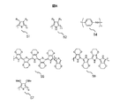
情報層に用いる導電性高分子エレクトロクロミック材料としては,図6に示す,ポリチオフェン51,ポリピロール52,ポリアニリン54,ポリ(3,4−エチレンジオキシチオフェン)55,ポリ(3,4−エチレンジオキシピロール)56,ポリ(3,4−エチレンジメトキシチオフェン)57などの導電性高分子およびそれらの,ポリスチレンスルホン酸,ポリビニルスルホン酸などとのイオン複合体が使用可能である。即ち、導電性高分子エレクトロクロミック材料は,ポリチオフェンおよびその誘導体,ポリピロールおよびその誘導体,ポリアニリンおよびその誘導体の中から選ばれた少なくとも1つの化合物を含むものである。ここで,図6中のnは整数,R1,R2,R3およびR4は,水素原子またはアルキル基,アルキルエーテル基,カルボキシル基などを表す。ポリチオフェン51,ポリピロール52において,置換基R1がブチル基,ヘキシル基,オクチル基,デシル基,のようなアルキル基の中から選ばれたものである場合には,有機溶剤に可溶であるので,キャストや回転塗布による情報層の形成に適する。また,上記導電性高分子とポリスチレンスルホン酸のイオン複合体は水溶性であり,キャストや回転塗布による情報層の形成に適する。情報層の形成は,導電性高分子エレクトロクロミック材料を水または有機溶剤に溶解してキャスティングや回転塗布する方法,蒸着,モノマーを用いた電極上での電界重合によって行うことが可能である。情報層は,電極上に形成した電解質層の上に,回転塗布や蒸着などによって積層してもよい。情報層は,消色状態での光透過率が90%以上,着色状態での光透過率が60%以下であることが望ましい。情報層の厚さは,100nm以下が望ましい。
【0024】
電解質層には,液体電解質,ゲル電解質および固体電解質が使用可能である。しかし,液体電解質,ゲル電解質の場合には導電性に優れるが,機械強度が乏しいため,スペーサや封止の機構が必要である。そのため,薄膜化が困難であり,かつ製造コストが高くなるので,固体電解質の方が望ましい。なお、液体電解質,ゲル電解質を用いた場合には、応答速度が速くなるというメリットがある。固体電解質は,支持媒体であるイオン伝導性高分子と,情報層へのドーパントとしての電解質塩から形成される。ここで用いるイオン伝導性高分子としては,ポリ(メチルメタクリレート),ポリエチレンオキサイド,ポリプロピレンオキサイド,エチレンオキサイドとエピクロロヒドリンの共重合体,ポリカーボネート,ポリシロキサンなどが挙げられる。電解質塩としては,過塩素酸リチウム(LiClO4),リチウムトリフレート(CF3SO3Li),リチウムヘキサフルオロホスフェート(LiPF6),リチウムテトラフルオロボレート(LiBF4),N−リチオトリフルオロメタンスルホンイミド(LiN(SO3CF3)2)などが使用可能である。電解質層のイオン伝導性を高めるため,プロピレンカーボネート,エチレンカーボネートなどの可塑剤,界面活性剤を加えても良い。
【0025】
電解質層の形成は,イオン伝導性高分子および電解質塩をアセトン,アセトニトリル,2−プロパノール,ジエチレングリコールジメチルエーテル,メチルエチルケトン,シクロヘキサノンなどの有機溶剤に溶解したものを回転塗布などによって電極上または情報層上に塗布した後に,溶剤を蒸発させて行なう。電解質層の厚さは,10nmから100nmの間であることが望ましい。
【0026】
情報層と,隣接した電解質層を挟む電極層には,ITO(indium tin oxide),酸化インジウム(In2O3),酸化スズ(SnO2),IZO(indium zinc oxide)などの金属酸化物,アルミニウム,金,銀,銅,パラジウム,クロム,プラチナ,ロジウムなどの金属が使用される。記録,再生光の入射する方向から見て,手前側の電極層には高い光透過率が要求され,85%以上の光透過率であることが望ましい。情報層の形成方法としては,RFスパッタリング,反応性スパッタリング,CVD(chemical vapor deposition),イオンプレーティング,真空蒸着と酸化処理,が挙げられる。
【0027】
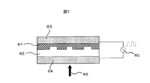
図1において,情報層1と電解質層2が隣接する界面に凹凸構造を作り,厚さの比率を部分的に変えたものを第1の電極63および第2の電極64で挟むと,たとえば,図7に示すような構造になる。このような構造では,第1の電極63と第2の電極64の間に電圧を印加すると,電解質層62中のイオンは電界の向きと水平方向に動く。したがって,情報層61の着色濃度は,情報層61の厚さとドーパントとしての電解質層62中のイオン量の比率に依存する。イオンの量が,情報層61を着色させるのに必要な量と比べて十分に多ければ,情報層61の厚さと着色濃度は正の相関,イオンの量が不足する場合には電解質層2の厚さのと着色濃度は負の相関がある。なお、ここでは、電解質層62、情報層61としたが、逆に電解質層を61,情報層を62のように逆に形成しても良い。
【0028】
電源65によって電圧を印加して,情報層を着色させると,情報層61の厚さと電解質層2の厚さに対応して光透過率(着色濃度)が異なる領域が生じるので,光66の反射を検出することにより,再生用の情報保持媒体としても使用できる。
【0029】
図8のように,片面に凹凸を有する電解質層72の凹部分に,情報層71を形成し,情報層71は電解質層72の凸部分によって分離され,それらが第1の電極73および第2の電極74で挟んだ構造は再生用の情報媒体として用いることができる。または、情報層77の凹部分に,情報層77の凸部分によって分離された電解質層78を形成し,第1の電極79および第2の電極80で挟んだ構造も同様に情報媒体として用いることができる。これらの図8の2種類の構造では,情報層と電解質層の両方が1対の電極で挟まれている部分は電圧印加時に着色するが,どちらか一方しか存在しない部分は着色しないので,光76の反射により情報を再生できる。
【0030】
本発明の情報保持媒体は,情報層に電流を供給する機構を記録再生装置に持たせて,CD−RやDVD−Rのような,光ディスクの形態で使用するのに適している。このときの媒体の構成を図9に示す。光は図面の上側から入射するように図示した。媒体は,光入射側101から,基板97,保護層91,透明電極である第1の電極層92,電解質層93,情報層94,第2の電極層95,紫外線硬化樹脂層96,貼り合せ保護基板97から構成され,99はグルーブ部,100はランド部に相当する。
【0031】
本発明では,基板の凹部で溝となっている部分をグルーブと呼ぶ。グルーブとグルーブの間をランドと呼ぶ。光が基板を通して膜に入射する場合は,入射側から見てグルーブは凸に見える。ランドとグルーブの一方だけに記録する,いわゆるイングルーブ記録の場合,光入射が基板側からの場合も基板と反対側からの場合も光入射側から見て凸部に記録した方が記録特性が良い場合が多いが,大きな差ではないので光入射側から見て凹部に記録しても良い。
【0032】
第1の電極と第2の電極のうち,少なくとも一方の電極を複数に分割して形成すると良い。放射状に複数に分割すればCAV(constant angular velocity)記録およびZCAV(zoned CAV)記録にも適合しやすく,電極間容量を小さくできるので応答速度を向上できる。
【0033】
本発明の情報保持媒体は,記録密度向上を図るための多層記録に適している。上記の単位構造を複数積層して,多層構造とすれば,記録密度向上による媒体の大容量化を達成できる。従来の媒体では,実効的記録密度(実効的面密度)を高めるには多層化が望ましいが,3層以上では各層の透過率と記録感度とがトレードオフの関係にあり,再生信号品質または記録感度のどちらかが犠牲にならざるを得なかった。透明有機材料に厚さ方向も含めて3次元記録するものも知られているが,2光子吸収を利用するものでは記録感度が非常に悪く,光重合を利用するものでは保存安定性と記録感度が悪い。しかし,本発明では,記録・再生時だけ,対象となる情報層が光吸収を有するので,対象以外の情報層が記録・再生の障害とならない。記録用あるいは読み出し用レーザ光の焦点移動で層選択を行なう,従来の複数層DVDのように,スペーサ層も必要ないので,多くの層を絞込みレンズの焦点深度内に配置することもでき,従来の複数層ディスクより多層・大容量化できる。焦点深度内に入らない情報層については,焦点位置を移動して記録・再生してもよい。その場合,多層積層するとアドレス情報を表わすピットや溝が変形する場合が有るが,場合によってはピットや溝を転写した層をたとえば中間に再度設けることにより,移動した焦点位置で焦点深度内の少なくとも一部の層のアドレスが読めるようにしておく必要が有る。
【0034】
積層は,図1の構造,図7の構造,および図8の2つの構造から選ばれた同種の構造の媒体で多層化しても良いし,異なる構造の媒体を組み合わせて多層化しても良い。再生用の媒体と,追記型の媒体を組み合わせることも可能である。
【0035】
本発明の情報保持媒体を光ディスクとして用いる際の記録の,記録線速度15m/s以上の条件でも記録レーザパワーを0.2mW以上2mW以下に設定することも可能となる。このように高感度化することにより,高線速度記録の場合でも,また,情報保持媒体上の複数の場所に同時に光照射を行う手段として,アレイレーザや面発光レーザを用いた場合でもパワー不足とならずに高い転送速度を実現できる。情報保持媒体の複数の電極対に対し,少なくとも2対同時に電圧を印加しても良い。これは,低い維持電圧を印加しておかないと色が変化する材料を用いた場合に必要となる。
【0036】
情報層を複数有する情報保持媒体を用い,多くの電極対間に電圧を印加するが,記録または読出し時に,それらを行う層の両側の電極間だけに他の電極間とは異なった電圧を印加するようにしても良い。
【0037】
また,記録または読み出しを行う際に,ある情報層から別の情報層に移動する場合には,記録または読み出しのためのレーザ照射をいったん止めてから電極に印加する電圧を変化させ,それまで記録または読み出しを行っていた層の消色と,新たに記録または読み出しを行う層の着色を行う。
【0038】
高速化のためには,記録または読み出し用のレーザ入射方向から見て手前側から奥側に移動する場合に限り,層切り替えによる待機時間短縮のために,手前側の層の記録または再生が終了して消色を行う以前に奥側の層の着色を開始してもよい。
【0039】
装置としては,ディスク回転モータの回転軸または回転軸に取付けられたディスク受け部品の,ディスク中心穴と接する部分に複数の電極が配置され,ディスク取り付け時にディスクの中心穴部の所定の各電極と相対するように位置決めする手段,および回転軸側電極とディスク側電極が接触する手段とを設ける。これによって,各電極に所定の電圧を印加することができる。
【0040】
そして,ディスクがセットされる高さの部分に複数に分割された電極が付加されているディスク回転モータの回転軸または回転軸に取付けられたディスク受け部品の側面の円周方向の少なくとも1ヶ所に,上下方向にテーパーの付いた突起が設けられていることを特徴とする情報記録装置とする。これによってディスクの回転方向の位置決めができて多層の電極に正確に給電することができる。
【0041】
本発明は2.6GB DVD−RAMの規格以上の記録密度(トラックピッチ,ビットピッチ)の場合に効果を発揮し,4.7GB DVD−RAMの規格以上の記録密度の場合に特に効果を発揮する。光源の波長が660nm付近でない場合や,集光レンズの開口数(NA)が0.6でない場合は,これらから半径方向,円周方向ともに波長比,NA比で換算した記録密度以上で効果を発揮し,発光波長約410 nmの青紫レーザを用いる場合においても効果がある。
【非特許文献1】Physical Review B,第28巻,No. 4,p. 2140−2145
【特許文献3】特開平11−185288号
【特許文献4】特開2002−184056号
【発明の実施の形態】
<実施例1>
(構成および製法)
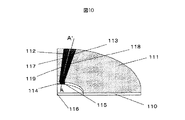
図10は,この発明の第1実施例のディスク状情報情報保持媒体の構造を示す図である。図10はディスクの1/4の構造図を示す。図10の上部の放射状透明電極は,同じ形状のものがディスク面を埋め尽くすように多数有るが,そのうち2本だけを描いている。記録・再生光は上方から基板を通して入射するが,図では最上部の基板は省略している。図11にはディスクの一部の拡大図を示す。通常は光スポットから見て凸の,グルーブと呼ばれる部分に記録・再生する場合が多いが,本実施例ではランド部に記録する場合を示す。図10の上部の電極の切れ目は,図10の放射状電極の間の隙間に対応している。A−A’ 断面の全体は,既に示した図9のようになっている。
【0042】
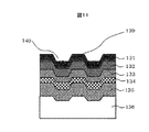
この媒体は次のようにして製作された。まず,図11に示すとおり,直径12cm,厚さ0.6mmで表面にトラックピッチが0.74μmで深さ23nmのイングルーブ記録(ここでは光スポットから見てランド記録)用のトラッキング用の溝(幅0.35μm)を有し,溝のウォブルによってアドレスが表現されたポリカーボネート基板136上に,(In2O3)90(SnO2)10の組成の透明電極(ITO)135(膜厚50nm)を形成した。基板表面への溝パターンの転写は,原盤のフォトレジストにメッキしたニッケルマスターから一度転写したマザーを用いて行った。フォトレジストに露光した溝がランドに対応するようにするためである。図11は基板上に製膜するプロセスを示す。この透明電極はマスクを用いたスパッタリングで形成することにより,記録セクターに対応して放射状の20の領域に分離されている。
【0043】
次に情報層134を平均膜厚100nmに形成した。情報層に用いた導電性高分子エレクトロクロミック材料は,ポリ(3,4−エチレンジオキシチオフェン)(0.5 重量%)とポリビニルスルホネート(0.8 重量%)の分散水溶液で,回転塗布装置により,回転数3000 rpm,2分間の条件で塗布を行なった後,ディジタルホットプレート上で100℃で5分間加熱して水を除去した。
【0044】
次に電解質層133を100nm形成した。ポリメチルメタクリレート(数平均分子量3万)(5重量%),プロピレンカーボネート(15重量%),過塩素酸リチウム(7重量%)のアセトニトリル溶液を回転塗布装置により,回転数1000 rpm,3分間の条件で塗布を行なった後,ディジタルホットプレート上で100℃で5分間加熱してアセトニトリルを除去した。
【0045】
電解質層133の上に,W80Ti20膜よりなる反射層兼第2の電極層132を膜厚50nmで形成した。積層膜の形成は,マグネトロン・スパッタリング装置を用いて行った。第2の電極の上には,UV樹脂を用いて厚さ0.5mmの保護層131を形成した。なお、図中、139はランド部140はグルーブ部である。
【0046】
透明電極のシート抵抗の影響や,グルーブの凹凸の角の部分で透明電極に膜厚の薄い部分ができることの影響で,外周部に電圧がかかりにくくなることを防ぐために,基板上に透明電極を付ける前に,図10に示す通り、放射状透明電極より幅の狭い,半径方向の平均の幅が約100μm,膜厚50nmから200nmの内周から外周に向かう細い金属(Al)電極118,119を,各放射状透明電極について1本設けた。この電極は,情報保持媒体にマスクを付けてスパッタリングによって形成した。記録・再生はこの電極の部分を避けて行う。なお、図中、110が基板、111が積層膜、112,113が透明電極、114,115は透明電極からの引き出し電極、116はディスク中心、117は電極間スペースである。
【0047】
本実施例とは逆に光スポットから見てグルーブに見える状態で記録するには,透明電極と反射層兼電極を逆にし,貼り合わせ基板側から光を入射させればよい。この場合,基板の成形はマザーでなく,ニッケルマスターを用いて行った。またこの場合,貼り合わせ基板を0.1mm程度に薄くして,絞込みレンズのNAを0.85と大きくしても良い。そうすればトラックピッチは約3/4の0.54μm程度にできる。
【0048】
透明電極とエレクトロクロミック材料層との間には1から5nm程度の膜厚のSiO2,GeO2など,Liよりもイオン半径が小さい元素の化合物膜を設けると,Liの透明電極中への侵入,透過を抑制できる点では好ましい。ただし,印加電圧は数ボルト高くする必要が有る。
【0049】
透明電極は複数の扇形透明電極に分離せず,ディスク全体が一電極でもよい。ただし,分離した方が電極間容量が小さくなるので,電圧の立上り,立下りが早くなって好ましい。発色,消色に要する時間と電流が実用的な範囲であるために電極間容量は0.1F以下が特に望ましいが,素子の特性が良好であるためには,0.01F以上となる構造とするのが良い。透明電極は複数の扇形電極に分離せず,金属電極の方を分離してもよい。また,上下の両電極を分離してもよい。この場合,上下の電極の切れ目の位置は一致していても良いが,一致していなくてもよい。
【0050】
反射層兼電極と上記透明電極には,それぞれの最内周部に引き出し電極を設け,この引出し電極はディスク最内周部まで達しており,図10に示すように,記録再生装置のディスク回転軸上のそれぞれ別の電極に接続するため,ディスク中心穴の端面の複数の電極114,115に接続されている。図12に示したように,ディスク受け用円板148を貫通するディスク回転モーターの回転軸141の側面のディスクがセットされる高さの部分には,実施例2で述べるような多層ディスクの場合5層までに対応できるように6個の分離した電極が接着されており(図では電極6個中3個145,146,147を示している),また,回転軸の円周上の一ヵ所では上下方向にテーパーのついた突起150または凹部があり,ディスクの中心穴の一ヵ所の凹部または凸部とのはめ合いで位置決めでき,所定の電極同士が接触する。ディスク回転軸の各電極には複数のブラシとリング142,143,144との組み合わせにより,記録装置の回路基板より給電される。給電方法は他の方法を用いても良い。
【0051】
記録・再生レーザ光は,基板側から入射した。最後に付ける電極層を透明電極とし,透明電極側,すなわち貼り合わせ基板側からレーザ光を入射させても良い。ただし,この場合,反射率が約10%となり,読出しのコントラスト比が得られるように記録膜膜厚を決めた。
【0052】
(エレクトロクロミック特性)
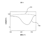
前記のようにして製作した情報保持媒体の情報層のエレクトロクロミック特性を評価した。図13は,情報層の可視域(波長500 nmから700 nm)の吸収スペクトルである。ディスク中央部の電極間に電圧を印加し始めてから1分後の,十分に定常状態に達した状態で測定した。電圧印加の方向は,互いに隣接しあう情報層と電解質層のうち,電解質層側を正とする。図13中,点線151で示した,電圧を印加していない時には,波長550nmから700nmにかけてほぼ完全に透明であるが,実線152で示した+3.0V印加時には,波長660nmを極大とする吸収帯が現れた。このときの波長660nmにおける透過率は40%であった。
【0053】
図14は,+3Vおよび−3Vの印加電圧切り替えに伴う波長660 nmにおける情報層の光透過率の時間変化を示す。この電圧切換は、10秒毎に行った。破線で示した153は,記録・再生に最低限必要な着色濃度である光透過率60%を示し,製作した情報保持媒体の情報層の着色濃度が十分であることが示された。消色の状態から,記録・読み出しに必要な着色濃度に達するまでの時間および着色状態から消色状態に戻るのに必要な時間はともに,約1秒であった。
【0054】
(記録・再生)
上記情報保持媒体に対して,情報の記録再生を行った。以下に,図15を用いて,本情報記録再生の動作を説明する。まず,記録再生を行う際のモータ制御方法としては,記録再生を行うゾーン毎にディスクの回転数を変化させるZCAV(Zoned Constant Linear Ve1ocity)方式を採用したものについて述べる。図15中、166はプリアンプ回路、167はL/Gサーボ回路、168はモータ、169は信号入力、170は信号出力を示す。
【0055】
記録装置外部からの情報は8ビットを1単位として,8−16変調器161に伝送される。情報保持媒体(以下,光ディスクと呼ぶ)160上に情報を記録する際には,情報8ビットを16ビットに変換する変調方式,いわゆる8−16変調方式を用いて記録が行われた。この変調方式では媒体上に,8ビットの情報に対応させた3T〜14Tのマーク長の情報の記録を行っている。図中の8−16変調器161はこの変調を行っている。なお,ここでTは情報記録時のクロックの周期を表している。ディスクは光スポットとの相対速度が約8m/sの線速度となるよう回転させた。
【0056】
8−16変調器161により変換された3T〜14Tのデジタル信号は記録波形発生回路162に転送され,マルチパルス記録波形が生成される。
【0057】
この際,記録マークを形成するためのパワーレベルを5mW,記録マークの消去が可能な中間パワーレベルを2mW,パワーを下げたパワーレベルを0.1mWとした。記録マーク形成のレーザパワーは,印加電圧を上げてゆくと下げることができ,0.5mW以上5mW以下の範囲で良好な記録が行えた。線速度を8m/sから変えても,この範囲に大きな変化は無かった。読出しは,電圧を印加せずに1mWで行った。0.2mW以上2mW以下の範囲で実用的な読出しが行えた。2mWを越えるパワーで長時間読むと,記録されているデータの劣化が生じた。また,上記記録波形発生回路内において,3T〜14Tの信号を時系列的に交互に「0」と「1」に対応させるようにしている。この際,高パワーレベルのパルスが照射された領域はエレクトロクロミック性が低下し,着色が起こりにくくなる。また,上記記録波形発生回路162内は,マーク部を形成するための一連の高パワーパルス列を形成する際に,マーク部前後のスペース部の長さに応じてマルチパルス波形の先頭パルス幅と最後尾のパルス幅を変化させる方式(適応型記録波形制御)に対応したマルチパルス波形テーブルを有しており,これによりマーク間に発生するマーク間熱干渉の影響を極力排除できるマルチパルス記録波形を発生している。
【0058】
記録波形発生回路162により生成された記録波形は,レーザ駆動回路163に転送され,レーザ駆動回路163はこの記録波形をもとに,光ヘッド164内の半導体レーザを発光させる。
【0059】
本記録装置に搭載された光ヘッド164には,情報記録用のレーザビームとして光波長660nmの半導体レーザが使用されている。また,このレーザ光をレンズNA0.65の対物レンズにより上記光ディスク160の情報層上に絞り込み,レーザビームを照射することにより情報の記録を行った。
【0060】
また,導電性高分子エレクトロクロミック材料を用いた情報層の場合,媒体の反射率は着色状態の方が高く,記録されて着色しなくなった状態の領域の反射率が低くなっている。レーザ光照射による記録の間,情報層の上下の電極間には3ボルトの電圧が継続的に印加される。
【0061】
本実施例の情報保持媒体構造では,グルーブの部分だけで上下の電極が近接しているため,記録膜に高電界がかかる範囲が狭い。従って,光スポットの位置や集光度が多少変わっても同じように記録され,AF,トラッキングのズレに寛容で,光に対して高感度であるだけでなく,この面でも高速回転記録に適している。
【0062】
また,本実施例の情報保持媒体では,記録マークとそれ以外の部分とで約2:1の光反射率のコントラスト比が得られた。コントラスト比がこれ以下になると,再生信号のノイズによる揺らぎが上限値の9%を越えてしまい,実用的な再生信号品質の範囲を外れる。透明電極にSiO2を含有させて(SiO2)40(In2O3)55(SnO2)5とすると,電極層の屈折率が低下して光学的に有利になり,コントラスト比は2.5:1にできた。
【0063】
同一,または別々の記録トラックに,単一の光ヘッドからまたは複数の光ヘッドから複数の光スポットを形成し,同時に記録することも容易に行える。
【0064】
本記録装置はグルーブとランドのうちランドに情報を記録する方式(いわゆるイングルーブ記録方式の変則版)に対応している。
【0065】
記録された情報の再生も上記光ヘッドを用いて行った。レーザビームを記録されたマーク上に照射し,マークとマーク以外の部分からの反射光を検出することにより,再生信号を得る。この再生信号の振幅をプリアンプ回路により増大させ,8−16復調器165では16ビット毎に8ビットの情報に変換する。以上の動作により,記録されたマークの再生が完了する。
【0066】
以上の条件でマークエッジ記録を行った場合,最短マークである3Tマークのマーク長は約0.20μm,最長マークである14Tマークのマーク長は約1.96μmとなる。記録信号には,情報信号の始端部,終端部に4Tマークと4Tスペースの繰り返しのダミーデータが含まれている。始端部にはVFOも含まれている。
【0067】
(マークエッジ記録)
DVD−RAMおよびDVD−RWには高密度記録が実現できるマークエッジ記録方式が採用されている。マークエッジ記録とは,記録膜に形成する記録マークの両端の位置をディジタルデータの1に対応させるもので,これにより,最短記録マークの長さを基準クロック1個でなく2〜3個分に対応させて高密度化することもできる。DVD−RAMでは8−16変調方式を採用しており,基準クロック3個分に対応させている。マークエッジ記録方式は,円形記録マークの中心位置をディジタルデータの1に対応させるマークポジション記録に比べると,記録マークを極端に小さくしなくても高密度記録できるという長所がある。ただし,記録マークの形状歪みが小さいことが情報保持媒体に要求される。
【0068】
(ZCLV記録方式,CAV記録方式)
導電性高分子エレクトロクロミック材料を用いた情報保持媒体では,記録波形を変えない場合,良好な記録再生特性を得るために,最適線速度で記録するのが望ましい。しかし,ディスク上の半径の異なる記録トラック間をアクセスする時,線速度を同じにするために回転数を変えるのには時間がかかる。そこでDVD−RAMでは,アクセス速度が小さくならないようにディスクの半径方向を24のゾーンに分け,ゾーン内では一定回転数とし,別のゾーンにアクセスしなければならない時だけ回転数を変えるZCLV(Zoned Constant Linear Velocity)方式を採用している。この方式では,ゾーン内の1番内周のトラックと一番外周のトラックで線速度が少し異なるので記録密度も少し異なるが,ディスク全域にわたってほぼ最大の密度で記録することができる。
【0069】
一方,半径方向に大きくアクセスしても回転数を変えなくても良い点では回転数一定のCAV記録方式が好ましく,回転数を変える際の電力消費を抑制できるのでモバイル機器にも適している。本発明は既に述べたように半径方向位置によらず一定の加熱時間が得られるので,CAV記録も容易にする効果が有る。
【0070】
(電極材料)
電極材料としては,記録レーザ光の波長において吸収がない,すなわち透明であるという光学特性が重要である。透明電極の材料としては,(In2O3)x(SnO2)1−xの組成で,xが5%から99%の範囲の材料,抵抗値の面でより好ましくは,xが90%から98%の範囲の材料,これにモル%で50%以下のSiO2を添加したもの,SnO2にモル%で2から5%のSb2O3などの他の酸化物を添加したものが使用可能である。また,フッ素をドープしたSnO2は,低抵抗かつ光透過率も高く,使用できる。あるいは,IZO(indium zinc oxide)は,表面の凹凸が少なく製膜できる利点があるので,電極層に使用可能である。レーザ光の情報保持媒体への入射側から見て奥側の電極層には,高い透明性は必ずしも要求されないので,光ディスク用に好ましい金属も使用可能である。反射率と熱伝導率が高い金属層は,AlあるいはAl合金の場合,Cr,Tiなどの添加元素が4原子%以下の高熱伝導率材料であるのが,基板表面の温度上昇を防止する効果があって好ましい。次いで,Au,Ag,Cu,Ni,Fe,Co,Cr,Ti,Pd,Pt,W,Ta,Mo,Sb,Bi,Dy,Cd,Mn,Mg,Vの元素単体,またはAu合金,Ag合金,Cu合金,Pd合金,Pt合金,Sb−Bi,SUS,Ni−Cr,などこれらを主成分とする合金,あるいはこれら同志の合金よりなる層を用いてもよい。このように,電極兼反射層は,金属元素,半金属元素,これらの合金,混合物,からなる。この中で,Cu,Ag,Au単体あるいはCu合金,Ag合金,特にPd,Cuなどの添加元素が8原子%以下のもの,Au合金等のように熱伝導率が大きいものは,有機材料の熱劣化を抑制する。可視域に吸収帯を持たない,狭バンドギャップ構造を有するポリチオフェン誘導体,ポリピロール誘導体,ポリアセチレンなどの導電性有機材料も使用可能である。
【0071】
(基板)
本実施例では,表面に直接,トラッキング用の溝を有するポリカーボネート基板を用いた。トラッキング用の溝を有する基板とは,基板表面全面または一部に,記録・再生波長をλとしたとき,λ/15n(nは基板材料の屈折率)以上の深さの溝を持つ基板である。溝は一周で連続的に形成されていても,途中分割されていてもよい。溝深さが約λ/12nの時,トラッキングとノイズのバランスの面で好ましいことがわかった。また,その溝幅は場所により異なっていてもよい。溝部とランド部の両方に記録・再生が行えるフォーマットを有する基板でも,どちらか一方に記録を行うフォーマットの基板でも良い。グルーブのみに記録するタイプでは,トラックピッチが波長/絞込みレンズのNAの0.7倍付近,グルーブ幅がその1/2付近のものが好ましい。
【0072】
(記録レーザパワー)
本実施例の情報保持媒体では,例えば,記録線速度8m/s以上の条件では,記録レーザパワーを10mWに設定した。
【0073】
(読出しレーザパワー)
読出しレーザパワーは,1mWに設定した。
【0074】
レーザ光源に,例えば4素子のアレーレーザを用いた場合,データ転送速度を4倍高速化することができる。
【0075】
(導電性高分子エレクトロクロミック材料)
情報層に用いる導電性高分子エレクトロクロミック材料として,ポリ(3,4−エチレンジオキシピロール),ポリ(3−ヘキシルピロール)を用いた場合でも,記録,再生を行なうことができた。
【0076】
しかし,導電性高分子エレクトロクロミック材料としては,Li+に代表されるドナーのドーピングを受けやすく,かつ,中性状態での酸化に対する安定性に優れているポリチオフェンおよびポリチオフェン誘導体の方がより優れている。ポリ(3,4−エチレンジオキシチオフェン)の代わりに,ポリチオフェン,ポリ(3,4−プロピレンジオキシチオフェン),ポリ(3,4−ジメトキシチオフェン),ポリ(3−ヘキシルチオフェン)を用いた情報保持媒体の場合でも,同様に記録・再生を行なうことができた。
【0077】
(電解質層の材料)
電解質層に用いる高分子として,ポリ(メチルメタクリレート)の代わりに,ポリエチレンオキサイド,ポリプロピレンオキサイド,エチレンオキサイドとエピクロロヒドリン(70:30)共重合体,ポリカーボネート,ポリシロキサンを用いた情報保持媒体の場合でも,同様に,記録・再生を行なうことができた。
【0078】
電解質塩として,過塩素酸リチウムの代わりに,リチウムトリフレート,リチウムヘキサフルオロホスフェート,リチウムテトラフルオロボレート,N−リチオトリフルオロメタンスルホンイミドを用いた場合でも,同様に,記録・再生を行なうことができた。
【0079】
<実施例2>
本実施例は,短波長レーザを記録・読み出しに使用可能にした情報保持媒体に関するものである。媒体の構造および作製方法は実施例1と同じである。
【0080】
直径12cm,厚さ0.6mmで表面にトラックピッチが0.45μmで深さ23nmのイングルーブ記録(ここでは光スポットから見てランド記録)用のトラッキング用の溝(幅0.25μm)を有し,溝のウォブルによってアドレスが表現されたポリカーボネート基板上に,SnO2の組成の透明電極(膜厚30nm)を形成した。基板表面への溝パターンの転写は,原盤のフォトレジストにメッキしたニッケルマスターから一度転写したマザーを用いて行った。この透明電極はマスクを用いたスパッタリングで形成し,記録セクターに対応して放射状の20の領域に分離した。
【0081】
次に情報層を膜厚100nmに形成した。情報層に用いた導電性高分子エレクトロクロミック材料は,ポリ(3,4−ジメトキシチオフェン)(0.5 重量%)とポリビニルスルホネート(0.8 重量%)の分散水溶液で,回転塗布装置により,回転数3000 rpmの条件で塗布を行なった後,ディジタルホットプレート上で100℃で5分間加熱して溶剤を除去した。
【0082】
次に電解質層を100nm形成した。ポリメチルメタクリレート(数平均分子量3万)(5重量%),プロピレンカーボネート(15重量%),過塩素酸リチウム(7重量%)のシクロヘキサノン溶液を回転塗布装置により,回転数3000 rpmの条件で塗布を行なった後,ディジタルホットプレート上で100℃で5分間加熱してシクロヘキサノンを除去した。電解質層の上に,W80Ti20膜よりなる反射層兼第2の電極層を膜厚50nmで形成した。積層膜の形成は,マグネトロン・スパッタリング装置を用いて行った。第2の電極の上には,UV樹脂を用いて厚さ0.5mmの保護層を形成した。
【0083】
図16は,本実施例の情報保持媒体の第1および第2の,1対の電極間に電圧を印加したときの吸収スペクトルである。電圧を印加し始めてから1分後の,十分に定常状態に達した状態で測定した。電圧印加の方向は,互いに隣接しあう情報層と電解質層のうち,電解質層側を正とする。図16中で点線171は−1.0V印加時のスペクトルであり,実線172は,+3.0V印加時のスペクトルである。+3.0V印加時には,波長400nm付近に吸収帯が現れた。従って,本媒体は波長400nmの青紫半導体レーザを用いた記録に適している。
【0084】
実施例1と同様に,図15の方法に従って,作製した情報保持媒体の記録再生を行った。
情報記録用のレーザビームとして光波長400nmの半導体レーザを使用した。また,このレーザ光をレンズNA0.65の対物レンズによって情報層上に絞り込み,強度6mWのレーザビームを照射することにより情報の記録を行った後,強度0.5mWのレーザビームによって再生を行うことができた。
【0085】
導電性高分子エレクトロクロミック材料に,ポリ(3,4−エトキシチオフェン),ポリ(3−ブチルチオフェン)を用いた情報保持媒体の場合にも同様に記録・再生を行なうことができた。
【0086】
<実施例3>
本実施例は多層構造情報保持媒体およびそれを用いる記録装置に関するものである。
【0087】
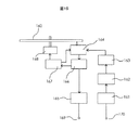
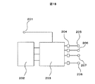
図17に,本実施例の記録装置の回転軸付近の構造,図18に記録装置制御回路のブロック図を示した。記録装置からは,回転軸の3本のスリップリング182,183,184に,電圧と,情報保持媒体の層の選択信号が供給される。コンデンサを含む図18の回路はディスク受け部品188の中空内部に内蔵されており,印加電圧切替え・制御回路を経て回路ブロック図の右端の各層への配線は,回転軸の電極185,186,187に接続されている。図18中、201は層選択信号、202は可変電源、203は層選択回路、204は電流制御器、205は第1層選択の信号、206は第2層選択の信号、207は第3層選択の信号、208は第4層選択の信号である。図17で、電極は8本有るが,他の5本は回転軸の見えていない面にあるので省略してある。これにより,着色させるべき層にはプラス電圧,消色する際にはマイナス電圧が印加される。図17中、181は回転軸、185は第1の接触電極、186は第2の接触電極、187は第3の接触電極、189は絶縁体、190は位置決め用凸部である。
【0088】
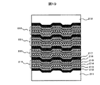
情報保持媒体は,実施例1と基本構造は同じである。図19に示したように,直径12cm,厚さ0.6mm,表面にトラックピッチが0.74μmで深さ23nm,溝幅0.35μmのイングルーブ記録用のトラッキング用の溝を有し,アドレス情報を上記溝のウォブルとして有するポリカーボネート基板211上に,SiO2層(10nm)212,IZO透明電極(30nm)213,情報層(80nm)214,電解質層(80nm)215,IZO透明電極(30nm)216,の順で第1層219を形成した。その上に,ZnS・SiO2絶縁層(100nm)217を形成した後,同様にして第2層220,第3層221,および第4層222を形成し,さらにこの上に直径120mm厚さ0.6mmのポリカーボネート基板218を貼り付けた。光はこの貼り合せ基板側から入射させた。
情報層214,電解質層215に使用した材料は,実施例1と同じである。
【0089】
記録・再生方法は実施例1と同様である。波長660nmのレーザ光を照射しながら,記録または読出しをしたい情報層の両側の透明電極に電圧を印加すると,その層だけが着色し,レーザ光を吸収,反射するようになるので,選択的に情報の記録や読出しができた。
【0090】
多層膜はすべて絞り込みレンズの焦点深度内に有っても良いが,厚さ20〜40μmのスペーサ層を数層毎(例えば3層おき)に挟んで焦点位置を変えて各層に記録・再生してもよい。この場合,スペーサ層を2層以上用いる場合は,光学系に球面収差を補償する素子を設けた方が良い。
【0091】
<実施例4>
本実施例は,情報再生専用媒体に関するものである。図20に本実施例の媒体の構造を示す。
【0092】
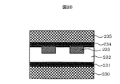
直径12cm,厚さ0.6mmのポリカーボネート基板230表面に,射出成形時に最小ピット長0.4μm,深さ90nmの,情報を表す凹凸構造を形成した後,反射層である厚さ50nmのAg94Pd4Cu2の層とITO透明電極(厚さ50nm)231をスパッタリング法で形成した。次にエレクトロクロミック層232を塗布により形成した。この凹凸構造が,再生専用(ROM)情報を含む。エレクトロクロミック層には,ポリ(3−ブチルチオフェン−2,5−ジイル)と,ポリスチレンスルホン酸の1:1(モル比)複合体を使用した。次に,ポリエチレンオキサイド(数平均分子量3万)(5重量%),エチレンカーボネート(25重量%),過塩素酸リチウム(3重量%)のアセトニトリル溶液を回転塗布機を用いて塗布し,エレクトロクロミック層232の凹凸を埋めるようにして電解質層233を形成した。その上に,上部ITO透明電極(50nm)234を形成した後,紫外線硬化樹脂保護コートをして,直径120mm厚さ0.6mmのポリカーボネート基板235を貼り付けた。波長660nmの情報再生用レーザ光はこの張り合わせ基板側から入射させた。エレクトロクロミック層および電解質層の基板凸部における膜厚は20から30nmであった。基板凹部では両方の層の膜厚が厚くなっている。
【0093】
2つのITO透明電極231および234間に,ITO透明電極234側を正として+5Vの電圧を印加したときに,電解質層が厚く存在する領域が着色し,強度1mWのレーザ光照射により情報を再生することができた。
【0094】
また,図20に示した情報再生用媒体と同じ材料と作製法で,凹凸基板上にITO透明電極,エレクトロクロミック層,電解質層,透明電極の順に形成し,次に厚さ約15nmの紫外線硬化シートを被せ,紫外線を照射してから上にスタンパーを配置して加熱ローラーを通過させることによりスタンパーを押し付けてスタンパーの表面の情報を表す凹凸をシート表面に転写し,続いて硬化させ,次に上記と同様にしてITO透明電極層のスパッタリングによる形成,エレクトロクロミック材料層塗布,電解質材料塗布,上部のITO透明電極層のスパッタリングを行った。シート被せ以降を4回繰り返し行い,紫外線硬化樹脂の保護コートをした後ポリカーボネート基板貼り合わせを行い,4層の再生専用媒体を作製した。実施例3に記載の記録・再生装置および制御回路を用いて層選択再生を行なった。光学系には球面収差補償素子を用いた。各層の再生信号のS/Nはいずれも46dB以上であり,良好な再生信号が得られることがわかった。
【0095】
さらに,前記シート被せの代わりに,液状UV樹脂を厚さ1μmになるように回転塗布した後,そこにUV照射を行なって硬化させる方法を用いて,同様に4層の再生専用媒体を作製した。また,前記シート被せあるいはUV樹脂層のいずれも用いず,(1)ITO透明電極層,(2)電解質層塗布,(3)パターン転写,(4)凹部を埋めるようにエレクトロクロミック材料層塗布,引き続き(1)から(4)をあと3回繰り返し,4層の再生専用媒体を作製した。実施例3に記載の記録・再生装置および制御回路を用いて層選択再生を行なった。光学系には球面収差補償素子を用いた。各層の再生信号のS/Nはいずれも46dB以上であり,良好な再生信号が得られることがわかった。
【0096】
【発明の効果】
上記構成によれば、高速に記録可能な情報保持媒体、光情報記録方法,装置を得ることができる。
【図面の簡単な説明】
【図1】本発明の情報保持媒体の構造を示す図。
【図2】本発明の情報保持媒体の情報層に用いる導電性高分子エレクトロクロミック材料であるポリチオフェンの共鳴構造を説明する図。
【図3】ポリチオフェンにドーピングしたときの分子構造の変化を表した図。
【図4】非縮退系導電性高分子の電子状態をバンド構造によって表した図。
【図5】無機半導体の電子状態をバンド構造によって表した図。
【図6】本発明の情報保持媒体の情報層に用いる導電性高分子エレクトロクロミック材料の化学構造を示す図。
【図7】本発明の実施例における情報保持媒体の構造を示す図。
【図8】本発明の実施例における情報保持媒体の構造を示す図。
【図9】本発明の実施例における情報保持媒体の構造を示す図。
【図10】本発明の実施例における情報保持媒体の構造を示す図。
【図11】本発明の実施例における情報保持媒体の構造を示す図。
【図12】本発明の実施例の情報保持媒体をセットするディスクホルダー部分の電極を示す図。
【図13】本発明の実施例における情報保持媒体の情報層の吸収スペクトルを示す図。
【図14】本発明の実施例における情報保持媒体の情報層の印加電圧切り替えに伴う波長660 nmにおける光透過率の時間変化を示す図。
【図15】本発明の実施例の印加電圧制御回路のブロック図。
【図16】本発明の実施例における情報層の吸収スペクトルを示す図。
【図17】本発明の実施例の情報保持媒体をセットするディスクホルダー部分の電極を示す図。
【図18】本発明の実施例における媒体への印加電圧制御回路のブロック図
【図19】本発明の実施例における4層情報保持媒体の構造を示す図。
【図20】本発明の実施例における再生専用媒体の構造を示す図。
【図21】酸化タングステンの混合原子価状態における伝導帯の電子状態を示す図。
【符号の説明】
1:情報層
2:電解質層
3:第1の電極
4:第2の電極
5:電源
6:光
8:ポリチオフェンのアロマティック型構造
9:ポリチオフェンのキノイド型構造
12:ポリチオフェンの中性状態の分子構造
13:ポリチオフェンへのアクセプタドーピングによる1電子酸化反応
14:ポリチオフェンの1電子酸化状態の分子構造
15:緩和過程
16:ポーラロン状態
17:バイポーラロン状態
18:ポリチオフェンへのドナードーピングによる1電子還元反応
19:ポリチオフェンへのアクセプタドーピングによる1電子酸化反応
20:ポリチオフェンへのドナードーピングによる1電子還元反応
21:中性状態におけるバンド構造
22:価電子帯
23:伝導帯
24:禁制帯幅
25:電子のエネルギー
26:許容遷移
27:正のポーラロン状態におけるバンド構造
28:ポーラロン準位P+
29:ポーラロン準位P−
30:ポーラロン状態における許容遷移
31:バイポーラロン状態におけるバンド構造
32:バイポーラロン準位BP+
33:バイポーラロン準位BP−
34:バイポーラロン状態における許容遷移
40:電子のエネルギー
41:伝導帯
42:価電子帯
43:禁制帯
44:禁制帯幅
45:ドナー準位
46:伝導帯の底
47:アクセプタ準位
51:ポリチオフェン
52:ポリピロール
54:ポリアニリン
55:ポリ(3,4−エチレンジオキシチオフェン)
56:ポリ(3,4−エチレンジオキシピロール)
61:情報層
62:電解質層
63:第1の電極
64:第2の電極
65:電源
66:光
71:情報層
72:電解質層
73:第1の電極
74:第2の電極
75:電源
76:光
77:情報層
78:電解質層
79:第1の電極
80:第2の電極
81:電源
91:保護層
92:第1の電極層
93:電解質層
94:情報層
95:第2の電極層
96:紫外線硬化樹脂層
97:貼り合せ保護基板
98:基板
99:グルーブ部
100:ランド部
101:入射レーザ光
110:貼り合わせ基板
111:積層膜
112:透明電極
113:透明電極
114:透明電極からの引き出し電極
115:透明電極からの引き出し電極
116:ディスク中心
117:電極間スペース
118:細い金属電極
119:細い金属電極
131:保護層
132:第1の電極層
133:電解質層
134:情報層
135:第2の電極層
136:紫外線硬化樹脂層
139:ランド部
140:グルーブ部
141:回転軸
142:第1のスリップリング
143:第2のスリップリング
144:第3のスリップリング
145:第1の接触電極
146:第2の接触電極
147:第3の接触電極
148:ディスク受け部品
149:絶縁体
150:位置決め用凸部
151:印加電圧0 Vの時の情報層の可視吸収スペクトル
152:印加電圧+3.0 Vの時の情報層の可視吸収スペクトル
153:記録・再生に必要な着色濃度
160:光ディスク
161:8−16変調器
162:記録波形発生回路
163:レーザ駆動回路
164:光ヘッド
165:8−16復調器
166:プリアンプ回路
167:L/Gサーボ回路
168:モータ
169:信号入力
170:信号出力
171:印加電圧−1 Vの時の情報層の可視吸収スペクトル
172:印加電圧+3 Vの時の情報層の可視吸収スペクトル
181:回転軸
182:第1のスリップリング
183:第2のスリップリング
184:第3のスリップリング
185:第1の接触電極
186:第2の接触電極
187:第3の接触電極
188:ディスク受け部品
189:絶縁体
190:位置決め用凸部
201:層選択信号
202:可変電源
203:層選択回路
204:電流制御器
205:第1層選択の信号
206:第2層選択の信号
207:第3層選択の信号
208:第4層選択の信号
211:ポリカーボネート基板
212:SiO2層
213:IZO透明電極
214:情報層
215:電解質層
216:IZO透明電極
217:ZnS・SiO2絶縁層
218:ポリカーボネート基板
219:第1層
220:第2層
221:第3層
222:第4層
230:ポリカーボネート基板
231:ITO電極層
232:エレクトロクロミック層
233:電解質層
234:ITO電極層
235:ポリカーボネート基板
240:電子のエネルギー
241:タングステン原子(5価)のエネルギー準位
242:タングステン原子(6価)のエネルギー準位
243:原子価間遷移。[0001]
TECHNICAL FIELD OF THE INVENTION
The present invention relates to an information storage medium for recording and reproducing information using light, an information recording method, and an information recording device.
[0002]
[Prior art]
In the present specification, a medium for recording and reproducing information, such as an optical disk, is referred to as an information holding medium.
[0003]
2. Description of the Related Art Conventionally, there have been DVDs using a phase change film as a recording film, such as a DVD-RAM, and optical disks using an organic material as an information layer, such as a CD-R or a DVD-R. An optical disc using an organic material as an information layer has an information layer containing a dye that absorbs at the wavelength of a recording light source, and performs recording by changing the surface of a substrate in contact with the information layer by laser irradiation.
[0004]
2. Description of the Related Art Conventionally, as described in, for example, Japanese Patent Application Laid-Open No. 63-123202, a field effect type optical disc in which information is recorded on a phase change recording film by irradiating a laser beam while an electric field is applied to the recording film. It has been known. This is used in an element structure in which a phase change information layer such as a GeSbTe system is sandwiched between upper and lower electrodes. By applying an electric field to the recording film, phase change (crystallization) is promoted more than by laser light irradiation alone.
[0005]
Also, Japanese Patent Application Laid-Open No. 5-101454 discloses a WO which shows an optical intercalation effect or an optical deintercalation effect.3There is described an optical information recording medium in which a semiconductor film made of and an electrolyte film are arranged in contact with each other, and when irradiated with light, ions of the electrolyte film are taken into the optical semiconductor to change to a transparent state.
[Patent Document 1] JP-A-63-123232.
[Patent Document 2] JP-A-5-101454
[Problems to be solved by the invention]
However, in JP-A-5-101454 described above, a liquid electrolyte having a higher response speed than a solid electrolyte is used as an electrolyte membrane. However, as a result of the study by the present inventors, there was a problem that the time required for the transmitted light intensity of the cell to become 70% of the incident light intensity required at least several tens of seconds, and was extremely slow.
[0006]
An object of the present invention is to provide a high-speed optical information recording method, an information holding medium and an apparatus.
[0007]
[Means for Solving the Problems]
The configuration of the present invention for solving the above problems will be described below.
[0008]
The basic structure of the information storage medium of the present invention is a configuration as shown in the sectional structure of FIG. The basic unit is an
[0009]
Here, the conductive polymer electrochromic material is a polymer having semiconductor-like conductivity, and a material whose color (absorption spectrum) reversibly changes when a voltage is applied. Examples of the conductive polymer electrochromic material include polyacetylene, polyaniline, polypyrrole, polythiophene, and derivatives thereof, which are conjugated polymers connected by conjugated double bonds or triple bonds. The electrochromism of these conductive polymer electrochromic materials is based on the following principle. Here, polythiophene will be described as an example. FIG. 2 shows an electron resonance structure in the ground state of polythiophene, and two structures, an aromatic structure 8 and a quinoid structure 9, are possible. Among the aromatic type structure 8 and the quinoid type structure 9, the aromatic type structure 8 has lower energy and is not energetically equivalent, so that the ground state of polythiophene is not degenerate. Similarly, polyaniline, polypyrrole, polythiophene, polyphenylenevinylene, and the like other than polythiophene are non-degenerate conductive polymers whose ground state is not degenerated. The electrochromism of a non-degenerate conductive polymer is explained by the following polarons and bipolarons. C. Physical Review B, Vol. 28, No. 4, p. 2140-2145. FIG. 3 shows a change in molecular structure accompanying doping of polythiophene. When the acceptor is doped into the
[0010]
The relationship between polarons and bipolarons and electrochromism is illustrated by FIG. 4, in which the electronic state of a non-degenerate conductive polymer is represented by a band structure. Here, changes in the electronic state due to acceptor doping are shown. In the
[0011]
The band structure of a non-degenerate conductive polymer is completely different from the band structure of an inorganic semiconductor represented by a silicon-based material. FIG. 5 shows an electronic state of the inorganic semiconductor crystal in the vicinity of the lattice constant by a band structure. The upper part of the figure shows that the
[0012]
For example, in an N-type semiconductor in which a silicon crystal is doped with P, As, Sb which is a group V atom, one electron in the outermost shell of the group V atom is located at a
[0013]
On the other hand, in a P-type semiconductor in which a silicon crystal is doped with boron (B), which is a group III atom, the boron atom replaces the silicon atom, and an
[0014]
Tungsten oxide, which is a typical inorganic electrochromic material and has the properties of an inorganic semiconductor, is colorless (with intercalation of alkali metal ions such as hydrogen ions or lithium ions into the crystal lattice by voltage application). Or pale yellow) to dark blue reversibly. Such electrochromism of tungsten oxide is due to intervalence transition absorption in a mixed valence state in which hexavalent tungsten atoms are partially reduced to pentavalent, and can be described with reference to FIG. 240 indicates the energy of the electrons. The conduction band of tungsten oxide is constituted by 5d orbitals of tungsten atoms. In the mixed valence state, an
[0015]
Since the electrochromic property accompanying the doping of the non-degenerate conductive polymer is used for recording, the non-degenerate conductive polymer exhibiting electrochromism is particularly referred to herein as “conductive polymer electrochromic material”.
[0016]
In addition, as a result of a publicly known example investigation after the invention was completed, JP-A-11-185288 and JP-A-2002-184056 were found.
[0017]
JP-A-11-185288 describes a medium having an electrochromic layer. The electrochromic layer includes a colored layer made of a substance that causes an electrochemical reaction and an electrolyte layer made of an electrolyte that mediates the electrochemical reaction. Then, the irradiated light is reflected by the colored electrochromic layer. However, Japanese Patent Application Laid-Open No. H11-185288 does not specifically describe what kind of material is used for the electrochromic layer and uses the electrochromic layer as a reflective layer, which is different from the present application.
[0018]
Japanese Patent Application Laid-Open No. 2002-184056 describes a method of utilizing a recording head having electrodes and electrochromism generated only in a portion sandwiched between a recording layer and an electrode layer on the medium side. In JP-A-2002-184056, a Prussian blue film is used as a recording film, which is different from a film using a conductive polymer electrochromic material as in the present application. Japanese Patent Application Laid-Open No. 2002-184056 discloses a method in which a recording head having an electrode on its surface is brought into contact with a recording layer formed on an electrode layer to perform recording. Can not be converted.
[0019]
Here, an optical recording and reproducing method when the information layer is a single layer will be described with reference to FIG.
[0020]
The
[0021]
Once recorded, the area is no longer colored even under the condition that the unrecorded area is colored. Therefore, when reproducing a recording, when a voltage is applied between the
[0022]
The following four recording mechanisms are possible as a recording mechanism in which the electrochromic property is reduced by heat.
a. The rate of change into the polaron state and the bipolaron state due to doping is reduced by cutting of the conjugate portion of the electrochromic conductive polymer in the information layer, conversion from a double bond to a single bond, oxidation, and the like.
b. Due to a curing reaction or a crystallization reaction due to cross-linking or polymerization reaction in the electrolyte layer, the resistance locally increases, making it difficult for the information layer to be reversibly doped.
c. At the interface between the information layer and the electrode layer adjacent thereto, a chemical reaction such as thermosetting occurs, and the resistance value increases.
d. At the interface between the information layer and the electrolyte layer adjacent thereto, a chemical reaction such as thermosetting occurs, and the resistance value increases.
If at least one of the above a to d occurs, recording is possible, but if a plurality occurs at the same time, high sensitivity of recording can be achieved.
[0023]
As the conductive polymer electrochromic material used for the information layer, as shown in FIG. 6,
[0024]
A liquid electrolyte, a gel electrolyte, and a solid electrolyte can be used for the electrolyte layer. However, liquid electrolytes and gel electrolytes are excellent in conductivity, but have poor mechanical strength, and require a spacer and a sealing mechanism. For this reason, it is difficult to reduce the film thickness and the manufacturing cost is increased. Therefore, a solid electrolyte is preferable. When a liquid electrolyte or a gel electrolyte is used, there is an advantage that the response speed is increased. The solid electrolyte is formed from an ion conductive polymer as a supporting medium and an electrolyte salt as a dopant for the information layer. Examples of the ion conductive polymer used here include poly (methyl methacrylate), polyethylene oxide, polypropylene oxide, a copolymer of ethylene oxide and epichlorohydrin, polycarbonate, and polysiloxane. As the electrolyte salt, lithium perchlorate (LiClO)4), Lithium triflate (CF3SO3Li), lithium hexafluorophosphate (LiPF6), Lithium tetrafluoroborate (LiBF4), N-lithiotrifluoromethanesulfonimide (LiN (SO3CF3)2) Can be used. In order to increase the ion conductivity of the electrolyte layer, a plasticizer such as propylene carbonate or ethylene carbonate or a surfactant may be added.
[0025]
The electrolyte layer is formed by dissolving an ion conductive polymer and electrolyte salt in an organic solvent such as acetone, acetonitrile, 2-propanol, diethylene glycol dimethyl ether, methyl ethyl ketone, cyclohexanone, etc., and spin-coating on the electrodes or information layer. After that, the solvent is evaporated. Preferably, the thickness of the electrolyte layer is between 10 nm and 100 nm.
[0026]
ITO (indium tin oxide) and indium oxide (In) are provided on the information layer and the electrode layer sandwiching the adjacent electrolyte layer.2O3), Tin oxide (SnO)2), Metal oxides such as indium zinc oxide (IZO), and metals such as aluminum, gold, silver, copper, palladium, chromium, platinum, and rhodium. When viewed from the direction in which the recording and reproduction light is incident, the electrode layer on the near side is required to have a high light transmittance, and preferably has a light transmittance of 85% or more. Examples of the method for forming the information layer include RF sputtering, reactive sputtering, chemical vapor deposition (CVD), ion plating, vacuum deposition, and oxidation treatment.
[0027]
In FIG. 1, when an uneven structure is formed at the interface between the
[0028]
When a voltage is applied by the
[0029]
As shown in FIG. 8, an
[0030]
The information storage medium of the present invention is suitable for use in the form of an optical disk, such as a CD-R or DVD-R, having a mechanism for supplying a current to the information layer in a recording / reproducing device. FIG. 9 shows the configuration of the medium at this time. Light is shown as being incident from the top of the figure. From the
[0031]
In the present invention, a groove portion in a concave portion of a substrate is called a groove. The land between the grooves is called a land. When light enters the film through the substrate, the groove looks convex when viewed from the incident side. In the case of so-called in-groove recording, in which recording is performed on only one of the land and the groove, when the light is incident from the substrate side or from the opposite side of the substrate, recording on the convex portion when viewed from the light incident side has better recording characteristics. In many cases, it is good, but since there is no large difference, the information may be recorded in the concave portion when viewed from the light incident side.
[0032]
At least one of the first electrode and the second electrode is preferably divided into a plurality of parts. Radially dividing into a plurality of pieces makes it easy to adapt to CAV (constant angular velocity) recording and ZCAV (zoned CAV) recording, and can reduce the interelectrode capacity, thereby improving the response speed.
[0033]
The information storage medium of the present invention is suitable for multilayer recording for improving the recording density. By stacking a plurality of the above unit structures to form a multilayer structure, it is possible to increase the capacity of the medium by improving the recording density. In conventional media, it is desirable to increase the number of layers in order to increase the effective recording density (effective area density). However, for three or more layers, there is a trade-off between the transmittance of each layer and the recording sensitivity. Either sensitivity had to be sacrificed. It is also known to record three-dimensionally on a transparent organic material including the thickness direction, but the recording sensitivity using two-photon absorption is extremely poor, and the storage stability and recording sensitivity using photopolymerization are very poor. Is bad. However, in the present invention, the target information layer has light absorption only at the time of recording / reproducing, so that the information layer other than the target does not hinder the recording / reproducing. Unlike the conventional multi-layer DVD, which does not require a spacer layer as in the conventional multi-layer DVD in which the layer is selected by moving the focal point of the recording or reading laser beam, many layers can be arranged within the focal depth of the focusing lens. Multi-layer disc and multi-layer capacity. For information layers that do not fall within the depth of focus, recording / reproducing may be performed by moving the focal position. In such a case, the pits or grooves representing address information may be deformed when the layers are stacked, but in some cases, a layer in which the pits or grooves are transferred may be provided again, for example, in the middle, so that at least Some layer addresses need to be readable.
[0034]
The lamination may be performed by multi-layering a medium having the same type of structure selected from the structure shown in FIG. 1, the structure shown in FIG. 7, and the two structures shown in FIG. 8, or by combining media having different structures. It is also possible to combine a reproduction medium and a write-once medium.
[0035]
The recording laser power can be set at 0.2 mW or more and 2 mW or less even under the condition that the recording linear velocity is 15 m / s or more when the information holding medium of the present invention is used as an optical disk. By increasing the sensitivity in this way, power is insufficient even in the case of high linear velocity recording and in the case where an array laser or a surface emitting laser is used as a means for simultaneously irradiating light to a plurality of locations on the information storage medium. High transfer speed can be realized without any problem. At least two pairs of voltages may be simultaneously applied to the plurality of electrode pairs of the information storage medium. This is necessary when a material that changes color unless a low sustaining voltage is applied is used.
[0036]
A voltage is applied between many pairs of electrodes using an information storage medium having a plurality of information layers. However, during recording or reading, a voltage different from that between the other electrodes is applied only between the electrodes on both sides of the layer where the information is recorded or read. You may do it.
[0037]
When recording or reading, when moving from one information layer to another information layer, stop the laser irradiation for recording or reading, and then change the voltage applied to the electrodes. Alternatively, decoloring of a layer from which reading was performed and coloring of a layer on which recording or reading is newly performed are performed.
[0038]
For speeding up, only when moving from the near side to the far side when viewed from the recording or reading laser incident direction, recording or reproduction of the near side layer is completed to shorten the waiting time by layer switching. Before the decoloring, the coloring of the back layer may be started.
[0039]
As the device, a plurality of electrodes are arranged in a portion of the rotating shaft of the disk rotating motor or a disk receiving part mounted on the rotating shaft in contact with the center hole of the disk. Means are provided for positioning so as to face each other, and means for bringing the rotating shaft side electrode and the disk side electrode into contact with each other. Thus, a predetermined voltage can be applied to each electrode.
[0040]
At least one circumferential position on the side surface of a rotating shaft of a disk rotating motor or a disk receiving component attached to the rotating shaft, in which a plurality of divided electrodes are added to a portion where the disk is set. , An information recording apparatus characterized in that a projection with a taper in the vertical direction is provided. As a result, it is possible to position the disk in the rotation direction, and to accurately supply power to the multilayered electrode.
[0041]
The present invention is effective when the recording density (track pitch, bit pitch) is higher than the standard of 2.6 GB DVD-RAM, and is particularly effective when the recording density is higher than the standard of 4.7 GB DVD-RAM. . When the wavelength of the light source is not near 660 nm or when the numerical aperture (NA) of the condenser lens is not 0.6, the effect can be obtained at a recording density higher than the recording density calculated in terms of the wavelength ratio and the NA ratio in both the radial and circumferential directions. It is effective and is effective even when a blue-violet laser having an emission wavelength of about 410 nm is used.
[Non-Patent Document 1] Physical Review B, Vol. 4, p. 2140-2145
[Patent Document 3] JP-A-11-185288
[Patent Document 4] JP-A-2002-184056
BEST MODE FOR CARRYING OUT THE INVENTION
<Example 1>
(Structure and manufacturing method)
FIG. 10 is a diagram showing the structure of the disk-shaped information information storage medium according to the first embodiment of the present invention. FIG. 10 shows a structure diagram of a quarter of the disk. There are many radial transparent electrodes in the upper part of FIG. 10 having the same shape so as to fill the disk surface, but only two of them are drawn. The recording / reproducing light enters through the substrate from above, but the uppermost substrate is omitted in the figure. FIG. 11 shows an enlarged view of a part of the disk. Usually, recording / reproducing is often performed on a portion called a groove which is convex when viewed from the light spot, but this embodiment shows a case where recording is performed on a land portion. The cuts in the upper electrode in FIG. 10 correspond to the gaps between the radial electrodes in FIG. The entire A-A 'cross section is as shown in FIG.
[0042]
This medium was manufactured as follows. First, as shown in FIG. 11, a tracking groove for in-groove recording (here, land recording as viewed from a light spot) having a diameter of 12 cm, a thickness of 0.6 mm, a track pitch of 0.74 μm and a depth of 23 nm on the surface is used. (Width 0.35 μm) and (In) on the
[0043]
Next, the
[0044]
Next, an
[0045]
On the
[0046]
In order to prevent the voltage from being hardly applied to the outer periphery due to the influence of the sheet resistance of the transparent electrode and the formation of the thin portion on the transparent electrode at the corners of the groove irregularities, the transparent electrode is placed on the substrate. Before attachment, as shown in FIG. 10, thin metal (Al)
[0047]
In order to perform recording in a state in which the groove looks as seen from the light spot contrary to the present embodiment, the transparent electrode and the reflective layer / electrode may be reversed and light may be incident from the bonded substrate side. In this case, the substrate was formed using a nickel master instead of a mother. In this case, the bonded substrate may be thinned to about 0.1 mm, and the NA of the focusing lens may be increased to 0.85. In this case, the track pitch can be reduced to about /, that is, about 0.54 μm.
[0048]
When a compound film of an element having a smaller ionic radius than Li, such as SiO2 and GeO2, having a thickness of about 1 to 5 nm is provided between the transparent electrode and the electrochromic material layer, penetration and transmission of Li into the transparent electrode are achieved. This is preferable in that it can suppress However, the applied voltage needs to be several volts higher.
[0049]
The transparent electrode is not divided into a plurality of sector-shaped transparent electrodes, and the entire disk may be one electrode. However, it is preferable to separate the electrodes because the capacitance between the electrodes becomes smaller, so that the voltage rises and falls faster. It is particularly desirable that the inter-electrode capacitance be 0.1 F or less because the time and current required for coloring and decoloring are within the practical range. Good to do. The transparent electrode may not be separated into a plurality of sector electrodes, but may be separated from the metal electrode. Also, the upper and lower electrodes may be separated. In this case, the positions of the cuts between the upper and lower electrodes may coincide, but do not have to coincide.
[0050]
An extraction electrode is provided at the innermost periphery of each of the reflective layer / electrode and the transparent electrode, and the extraction electrode reaches the innermost periphery of the disk. As shown in FIG. In order to connect to each other electrode on the shaft, it is connected to a plurality of
[0051]
The recording / reproducing laser light was incident from the substrate side. The last electrode layer to be formed may be a transparent electrode, and laser light may be incident from the transparent electrode side, that is, the bonded substrate side. However, in this case, the recording film thickness was determined so that the reflectance was about 10% and a readout contrast ratio was obtained.
[0052]
(Electrochromic characteristics)
The electrochromic characteristics of the information layer of the information storage medium manufactured as described above were evaluated. FIG. 13 is an absorption spectrum of the information layer in the visible region (wavelength from 500 nm to 700 nm). One minute after starting to apply a voltage between the electrodes at the center of the disk, the measurement was performed in a state where a sufficiently steady state was reached. The direction of voltage application is positive on the electrolyte layer side of the information layer and the electrolyte layer adjacent to each other. In FIG. 13, when a voltage is not applied, almost completely transparent from a wavelength of 550 nm to 700 nm as indicated by a dotted
[0053]
FIG. 14 shows the change over time in the light transmittance of the information layer at a wavelength of 660 nm accompanying the switching of the applied voltage between +3 V and -3 V. This voltage switching was performed every 10 seconds. 153 indicated by a broken line indicates a light transmittance of 60%, which is the minimum coloring density required for recording / reproducing, indicating that the coloring density of the information layer of the manufactured information storage medium is sufficient. The time required to reach the color density required for recording / reading from the decolored state and the time required to return from the colored state to the decolored state were both about 1 second.
[0054]
(Record and playback)
Recording and reproduction of information were performed on the information holding medium. Hereinafter, the operation of the information recording / reproduction will be described with reference to FIG. First, as a motor control method at the time of recording / reproducing, a method adopting a ZCAV (Zone Constant Constant Velocity) system which changes the number of rotations of a disk for each zone where recording / reproducing is performed will be described. In FIG. 15,
[0055]
Information from the outside of the recording device is transmitted to the 8-16 modulator 161 in units of 8 bits. When recording information on an information storage medium (hereinafter, referred to as an optical disk) 160, recording was performed using a modulation method for converting 8 bits of information into 16 bits, a so-called 8-16 modulation method. In this modulation method, information having a mark length of 3T to 14T corresponding to 8-bit information is recorded on a medium. The 8-16 modulator 161 in the figure performs this modulation. Here, T represents a clock cycle at the time of information recording. The disk was rotated so that the relative speed with respect to the light spot became a linear speed of about 8 m / s.
[0056]
The 3T to 14T digital signal converted by the 8-16 modulator 161 is transferred to the recording
[0057]
At this time, the power level for forming the recording marks was 5 mW, the intermediate power level at which the recording marks could be erased was 2 mW, and the reduced power level was 0.1 mW. The laser power for forming the recording mark can be reduced by increasing the applied voltage, and good recording was performed in the range of 0.5 mW to 5 mW. Even if the linear velocity was changed from 8 m / s, there was no significant change in this range. Reading was performed at 1 mW without applying a voltage. Practical reading was performed in the range of 0.2 mW or more and 2 mW or less. Reading for a long time at a power exceeding 2 mW deteriorated the recorded data. In the recording waveform generating circuit, signals of 3T to 14T are made to correspond to "0" and "1" alternately in time series. At this time, the region irradiated with the high power level pulse has a reduced electrochromic property and is less likely to be colored. When forming a series of high-power pulse trains for forming a mark portion, the recording
[0058]
The recording waveform generated by the recording
[0059]
A semiconductor laser having a light wavelength of 660 nm is used as a laser beam for information recording in the
[0060]
Further, in the case of an information layer using a conductive polymer electrochromic material, the reflectance of the medium is higher in the colored state, and the reflectance in the recorded and uncolored area is lower. During recording by laser beam irradiation, a voltage of 3 volts is continuously applied between the upper and lower electrodes of the information layer.
[0061]
In the information storage medium structure of the present embodiment, the upper and lower electrodes are close to each other only in the groove portion, so that the range in which a high electric field is applied to the recording film is narrow. Therefore, even if the position of the light spot and the degree of condensing are slightly changed, the same recording is performed, which is not only tolerant to the deviation of AF and tracking and has high sensitivity to light, but also suitable for high-speed rotation recording in this aspect. I have.
[0062]
Further, in the information storage medium of this embodiment, a contrast ratio of a light reflectance of about 2: 1 was obtained between the recording mark and the other portions. If the contrast ratio is lower than this, the fluctuation due to the noise of the reproduction signal exceeds 9% of the upper limit value, which falls outside the range of the practical reproduction signal quality. SiO for transparent electrode2(SiO 22)40(In2O3)55(SnO2)5In this case, the refractive index of the electrode layer is reduced, which is optically advantageous, and the contrast ratio is 2.5: 1.
[0063]
A plurality of light spots can be formed on the same or different recording tracks from a single optical head or from a plurality of optical heads, and recording can be easily performed simultaneously.
[0064]
This recording apparatus is compatible with a method of recording information on a land out of a groove and a land (a variation of the so-called in-groove recording method).
[0065]
Reproduction of the recorded information was also performed using the optical head. A reproduction signal is obtained by irradiating a laser beam onto the recorded mark and detecting reflected light from the mark and a portion other than the mark. The amplitude of the reproduced signal is increased by a preamplifier circuit, and the 8-16
[0066]
When mark edge recording is performed under the above conditions, the mark length of the shortest mark 3T mark is about 0.20 μm, and the mark length of the longest mark 14T mark is about 1.96 μm. The recording signal includes dummy data of a repetition of a 4T mark and a 4T space at the start and end of the information signal. The start end also includes VFO.
[0067]
(Mark edge recording)
The DVD-RAM and the DVD-RW employ a mark edge recording method capable of realizing high-density recording. In the mark edge recording, the positions of both ends of the recording mark formed on the recording film correspond to one of the digital data, thereby reducing the length of the shortest recording mark to two or three instead of one reference clock. It is also possible to increase the density in correspondence. The DVD-RAM adopts the 8-16 modulation method, and corresponds to three reference clocks. The mark edge recording method has an advantage that high-density recording can be performed without making the recording mark extremely small as compared with mark position recording in which the center position of the circular recording mark corresponds to 1 of digital data. However, the information storage medium is required to have a small shape distortion of the recording mark.
[0068]
(ZCLV recording method, CAV recording method)
In the case of an information storage medium using a conductive polymer electrochromic material, it is desirable to record at an optimum linear velocity in order to obtain good recording / reproducing characteristics when the recording waveform is not changed. However, when accessing between recording tracks of different radii on a disk, it takes time to change the number of revolutions to make the linear velocity the same. Therefore, in a DVD-RAM, the radial direction of the disk is divided into 24 zones so that the access speed is not reduced, and a constant rotation speed is set in each zone, and the rotation speed is changed only when it is necessary to access another zone. (Constant Linear Velocity) method. In this method, the recording speed is slightly different because the linear velocity is slightly different between the innermost track and the outermost track in the zone, but it is possible to record at almost the maximum density over the entire area of the disk.
[0069]
On the other hand, the CAV recording method in which the rotation speed is constant is preferable in that it is not necessary to change the rotation speed even if a large access is made in the radial direction, and it is suitable for mobile devices because the power consumption when changing the rotation speed can be suppressed. . According to the present invention, a constant heating time can be obtained irrespective of the position in the radial direction, as described above.
[0070]
(Electrode material)
It is important for the electrode material to have an optical property that it has no absorption at the wavelength of the recording laser beam, that is, it is transparent. As a material of the transparent electrode, (In2O3) X (SnO2) A material having a composition of 1-x, wherein x is in the range of 5% to 99%, more preferably a material in which x is in the range of 90% to 98%, and a material having x in the range of 90% to 98%, and SiO2With SnO, SnO22-5% Sb in mole%2O3For example, those to which other oxides are added can be used. In addition, SnO doped with fluorine2Can be used because of its low resistance and high light transmittance. Alternatively, IZO (indium zinc oxide) can be used for an electrode layer because it has an advantage that a film can be formed with less surface irregularities. Since high transparency is not necessarily required for the electrode layer on the back side when viewed from the side where the laser beam enters the information holding medium, metals that are preferable for optical disks can also be used. In the case of Al or Al alloy, the metal layer having high reflectivity and thermal conductivity is a high thermal conductivity material containing 4 atomic% or less of additional elements such as Cr and Ti. Is preferred. Next, elemental elements of Au, Ag, Cu, Ni, Fe, Co, Cr, Ti, Pd, Pt, W, Ta, Mo, Sb, Bi, Dy, Cd, Mn, Mg, V, or an Au alloy, Ag Alloys containing these as main components, such as alloys, Cu alloys, Pd alloys, Pt alloys, Sb—Bi, SUS, Ni—Cr, or layers composed of alloys of these may be used. As described above, the electrode / reflection layer is composed of a metal element, a metalloid element, an alloy thereof, and a mixture. Among them, Cu, Ag, Au alone or a Cu alloy, an Ag alloy, particularly those having an additive element of 8 atomic% or less such as Pd and Cu, and those having a large thermal conductivity such as an Au alloy are those of organic materials. Suppress thermal degradation. Conductive organic materials such as polythiophene derivatives, polypyrrole derivatives, and polyacetylene having no bandgap in the visible region and having a narrow bandgap structure can also be used.
[0071]
(substrate)
In the present embodiment, a polycarbonate substrate having tracking grooves directly on the surface was used. A substrate having a groove for tracking is a substrate having a groove having a depth of λ / 15n (n is the refractive index of the substrate material) or more when the recording / reproducing wavelength is λ on the entire surface or a part of the substrate surface. is there. The groove may be formed continuously in one round or may be divided in the middle. It was found that when the groove depth was about λ / 12n, it was preferable in terms of the balance between tracking and noise. Further, the groove width may be different depending on the location. A substrate having a format in which recording / reproducing can be performed on both the groove and the land, or a substrate having a format in which recording can be performed on either one may be used. In the type in which recording is performed only in the groove, it is preferable that the track pitch is about 0.7 times the wavelength / NA of the focusing lens and the groove width is about 1/2 of that.
[0072]
(Recording laser power)
In the information storage medium of this embodiment, for example, the recording laser power was set to 10 mW under the condition that the recording linear velocity was 8 m / s or more.
[0073]
(Read laser power)
The read laser power was set to 1 mW.
[0074]
When a four-element array laser is used as the laser light source, the data transfer speed can be increased four times.
[0075]
(Conductive polymer electrochromic material)
Recording and reproduction could be performed even when poly (3,4-ethylenedioxypyrrole) or poly (3-hexylpyrrole) was used as the conductive polymer electrochromic material used for the information layer.
[0076]
However, as a conductive polymer electrochromic material, Li+The polythiophene and the polythiophene derivative, which are easily susceptible to doping of a donor represented by, and are excellent in stability against oxidation in a neutral state, are more excellent. Information using polythiophene, poly (3,4-propylenedioxythiophene), poly (3,4-dimethoxythiophene), poly (3-hexylthiophene) instead of poly (3,4-ethylenedioxythiophene) In the case of the holding medium, recording and reproduction could be performed similarly.
[0077]
(Material of electrolyte layer)
As a polymer used for the electrolyte layer, instead of poly (methyl methacrylate), an information storage medium using polyethylene oxide, polypropylene oxide, a copolymer of ethylene oxide and epichlorohydrin (70:30), polycarbonate, and polysiloxane. In this case, recording and reproduction could be performed similarly.
[0078]
Even when lithium triflate, lithium hexafluorophosphate, lithium tetrafluoroborate, or N-lithiotrifluoromethanesulfonimide is used instead of lithium perchlorate as an electrolyte salt, recording and reproduction can be performed in the same manner. Was.
[0079]
<Example 2>
This embodiment relates to an information storage medium in which a short-wavelength laser can be used for recording and reading. The structure and manufacturing method of the medium are the same as in the first embodiment.
[0080]
There is a tracking groove (width 0.25 μm) for in-groove recording (here, land recording viewed from the light spot) having a diameter of 12 cm, a thickness of 0.6 mm, and a track pitch of 0.45 μm and a depth of 23 nm on the surface. Then, the SnO is placed on the polycarbonate substrate whose address is expressed by the groove wobbles.2Was formed (
[0081]
Next, an information layer was formed to a thickness of 100 nm. The conductive polymer electrochromic material used for the information layer is an aqueous dispersion of poly (3,4-dimethoxythiophene) (0.5% by weight) and polyvinylsulfonate (0.8% by weight). After coating at 3000 rpm, the solvent was removed by heating at 100 ° C. for 5 minutes on a digital hot plate.
[0082]
Next, an electrolyte layer was formed to a thickness of 100 nm. A cyclohexanone solution of polymethyl methacrylate (number average molecular weight 30,000) (5% by weight), propylene carbonate (15% by weight), and lithium perchlorate (7% by weight) is applied by a spin coater at a rotation speed of 3000 rpm. After that, the mixture was heated at 100 ° C. for 5 minutes on a digital hot plate to remove cyclohexanone. On the electrolyte layer, W80Ti20A reflective layer and a second electrode layer made of a film were formed with a thickness of 50 nm. The formation of the laminated film was performed using a magnetron sputtering apparatus. On the second electrode, a protective layer having a thickness of 0.5 mm was formed using a UV resin.
[0083]
FIG. 16 is an absorption spectrum when a voltage is applied between the first and second pairs of electrodes of the information storage medium of the present example. One minute after the start of voltage application, the measurement was performed in a state where the steady state was sufficiently reached. The direction of voltage application is positive on the electrolyte layer side of the information layer and the electrolyte layer adjacent to each other. In FIG. 16, a
[0084]
In the same manner as in Example 1, recording / reproduction of the produced information storage medium was performed according to the method of FIG.
A semiconductor laser having a light wavelength of 400 nm was used as a laser beam for information recording. The laser beam is focused on the information layer with an objective lens having a lens NA of 0.65, and information is recorded by irradiating a laser beam having an intensity of 6 mW, and then reproduction is performed using a laser beam having an intensity of 0.5 mW. Was completed.
[0085]
Recording / reproducing could also be performed in the case of an information storage medium using poly (3,4-ethoxythiophene) or poly (3-butylthiophene) as the conductive polymer electrochromic material.
[0086]
<Example 3>
This embodiment relates to a multilayer information storage medium and a recording apparatus using the same.
[0087]
FIG. 17 shows the structure near the rotation axis of the recording apparatus of this embodiment, and FIG. 18 shows a block diagram of the recording apparatus control circuit. From the recording device, a voltage and a signal for selecting the layer of the information storage medium are supplied to the three
[0088]
The information storage medium has the same basic structure as that of the first embodiment. As shown in FIG. 19, a tracking groove for in-groove recording having a diameter of 12 cm, a thickness of 0.6 mm, a track pitch of 0.74 μm, a depth of 23 nm and a groove width of 0.35 μm on the surface is provided. On a
The materials used for the
[0089]
The recording / reproducing method is the same as in the first embodiment. When a voltage is applied to the transparent electrodes on both sides of the information layer on which recording or reading is to be performed while irradiating a laser beam having a wavelength of 660 nm, only that layer is colored and the laser beam is absorbed and reflected. Information could be recorded and read.
[0090]
Although all of the multilayer films may be within the focal depth of the aperture lens, recording / reproducing is performed on each layer by changing the focal position by interposing a spacer layer having a thickness of 20 to 40 μm every several layers (for example, every three layers). May be. In this case, when using two or more spacer layers, it is better to provide an element for compensating for spherical aberration in the optical system.
[0091]
<Example 4>
This embodiment relates to an information reproduction-only medium. FIG. 20 shows the structure of the medium of this embodiment.
[0092]
After forming an uneven structure representing information with a minimum pit length of 0.4 μm and a depth of 90 nm on the surface of a
[0093]
When a voltage of +5 V is applied between the two ITO
[0094]
In addition, using the same material and the same manufacturing method as the information reproducing medium shown in FIG. 20, an ITO transparent electrode, an electrochromic layer, an electrolyte layer, and a transparent electrode are formed in this order on an uneven substrate, and then UV-cured to a thickness of about 15 nm. Cover the sheet, irradiate ultraviolet rays, place the stamper on top, pass the heating roller, press the stamper, transfer the irregularities representing the information on the surface of the stamper to the sheet surface, then cure, then cure In the same manner as above, formation of the ITO transparent electrode layer by sputtering, application of an electrochromic material layer, application of an electrolyte material, and sputtering of the upper ITO transparent electrode layer were performed. The steps of covering the sheet and thereafter were repeated four times, a protective coat of an ultraviolet curable resin was applied, and then a polycarbonate substrate was bonded, thereby producing a four-layer read-only medium. Layer selection / reproduction was performed using the recording / reproduction device and the control circuit described in Example 3. A spherical aberration compensating element was used for the optical system. The S / N of the reproduction signal of each layer was 46 dB or more, and it was found that a good reproduction signal was obtained.
[0095]
Further, instead of the above-mentioned sheet covering, a liquid UV resin was spin-coated so as to have a thickness of 1 μm, and then UV irradiation was performed thereon to cure the resin, thereby similarly producing a four-layer read-only medium. . Further, without using the sheet covering or the UV resin layer, (1) ITO transparent electrode layer, (2) electrolyte layer coating, (3) pattern transfer, (4) electrochromic material layer coating so as to fill concave portions, Subsequently, (1) to (4) were repeated three more times to produce a four-layer read-only medium. Layer selection / reproduction was performed using the recording / reproduction device and the control circuit described in Example 3. A spherical aberration compensating element was used for the optical system. The S / N of the reproduction signal of each layer was 46 dB or more, and it was found that a good reproduction signal was obtained.
[0096]
【The invention's effect】
According to the above configuration, it is possible to obtain an information storage medium, an optical information recording method, and an apparatus capable of recording at high speed.
[Brief description of the drawings]
FIG. 1 is a diagram showing the structure of an information storage medium according to the present invention.
FIG. 2 is a diagram illustrating a resonance structure of polythiophene, which is a conductive polymer electrochromic material used for the information layer of the information storage medium of the present invention.
FIG. 3 is a diagram showing a change in molecular structure when polythiophene is doped.
FIG. 4 is a diagram showing an electronic state of a non-degenerate conductive polymer by a band structure.
FIG. 5 is a diagram showing an electronic state of an inorganic semiconductor by a band structure.
FIG. 6 is a view showing the chemical structure of a conductive polymer electrochromic material used for the information layer of the information storage medium of the present invention.
FIG. 7 is a diagram showing a structure of an information storage medium according to the embodiment of the present invention.
FIG. 8 is a diagram showing a structure of an information storage medium according to the embodiment of the present invention.
FIG. 9 is a diagram showing a structure of an information storage medium according to the embodiment of the present invention.
FIG. 10 is a diagram showing a structure of an information storage medium according to the embodiment of the present invention.
FIG. 11 is a diagram showing the structure of an information storage medium according to an embodiment of the present invention.
FIG. 12 is a diagram showing electrodes of a disk holder portion for setting an information holding medium according to the embodiment of the present invention.
FIG. 13 is a diagram showing an absorption spectrum of the information layer of the information storage medium in the example of the present invention.
FIG. 14 is a diagram showing a time change of the light transmittance at a wavelength of 660 nm accompanying the switching of the applied voltage of the information layer of the information storage medium in the example of the present invention.
FIG. 15 is a block diagram of an applied voltage control circuit according to the embodiment of the present invention.
FIG. 16 is a diagram showing an absorption spectrum of the information layer in the example of the present invention.
FIG. 17 is a view showing electrodes of a disk holder portion for setting an information holding medium according to the embodiment of the present invention.
FIG. 18 is a block diagram of a circuit for controlling a voltage applied to a medium according to an embodiment of the present invention.
FIG. 19 is a view showing the structure of a four-layer information storage medium according to an embodiment of the present invention.
FIG. 20 is a diagram showing the structure of a read-only medium according to the embodiment of the present invention.
FIG. 21 illustrates an electronic state of a conduction band in a mixed valence state of tungsten oxide.
[Explanation of symbols]
1: Information layer
2: Electrolyte layer
3: First electrode
4: Second electrode
5: Power supply
6: Light
8: Aromatic structure of polythiophene
9: Quinoid structure of polythiophene
12: Molecular structure of neutral state of polythiophene
13: One-electron oxidation reaction by acceptor doping of polythiophene
14: Molecular structure of one-electron oxidation state of polythiophene
15: Relaxation process
16: Polaron state
17: Bipolaron state
18: One-electron reduction reaction by donor doping to polythiophene
19: One-electron oxidation reaction by acceptor doping of polythiophene
20: One-electron reduction reaction by donor doping to polythiophene
21: band structure in neutral state
22: Valence band
23: conduction band
24: Forbidden band width
25: Electron energy
26: Allowable transition
27: Band structure in positive polaron state
28: Polaron level P+
29: Polaron level P-
30: Allowable transition in polaron state
31: Band structure in bipolaron state
32: Bipolaron level BP+
33: Bipolaron level BP-
34: Allowable transition in bipolaron state
40: Energy of electron
41: conduction band
42: Valence band
43: Forbidden belt
44: Forbidden band width
45: Donor level
46: bottom of conduction band
47: Acceptor level
51: Polythiophene
52: Polypyrrole
54: Polyaniline
55: poly (3,4-ethylenedioxythiophene)
56: Poly (3,4-ethylenedioxypyrrole)
61: Information layer
62: electrolyte layer
63: first electrode
64: second electrode
65: Power supply
66: Light
71: Information layer
72: electrolyte layer
73: first electrode
74: second electrode
75: Power supply
76: Light
77: Information layer
78: Electrolyte layer
79: first electrode
80: second electrode
81: Power supply
91: protective layer
92: first electrode layer
93: Electrolyte layer
94: Information layer
95: second electrode layer
96: UV curable resin layer
97: Lamination protection substrate
98: Substrate
99: Groove part
100: Land section
101: incident laser light
110: bonded substrate
111: laminated film
112: transparent electrode
113: Transparent electrode
114: Extraction electrode from transparent electrode
115: Extraction electrode from transparent electrode
116: Disc center
117: Space between electrodes
118: Thin metal electrode
119: Thin metal electrode
131: protective layer
132: first electrode layer
133: Electrolyte layer
134: Information Layer
135: second electrode layer
136: UV curable resin layer
139: Land section
140: Groove section
141: Rotary axis
142: First slip ring
143: Second slip ring
144: Third slip ring
145: first contact electrode
146: second contact electrode
147: Third contact electrode
148: Disc receiving part
149: Insulator
150: convex for positioning
151: Visible absorption spectrum of information layer at applied voltage of 0 V
152: visible absorption spectrum of the information layer at an applied voltage of +3.0 V
153: Color density required for recording / reproduction
160: Optical disk
161: 8-16 modulator
162: recording waveform generation circuit
163: Laser drive circuit
164: Optical head
165: 8-16 demodulator
166: Preamplifier circuit
167: L / G servo circuit
168: Motor
169: Signal input
170: signal output
171: Visible absorption spectrum of information layer at applied voltage of -1 V
172: visible absorption spectrum of the information layer when the applied voltage is +3 V
181: Rotation axis
182: First slip ring
183: Second slip ring
184: Third slip ring
185: first contact electrode
186: second contact electrode
187: Third contact electrode
188: Disc receiving part
189: Insulator
190: Positioning projection
201: layer selection signal
202: Variable power supply
203: Layer selection circuit
204: current controller
205: signal for selecting the first layer
206: Second layer selection signal
207: Third layer selection signal
208: fourth layer selection signal
211: polycarbonate substrate
212: SiO2layer
213: IZO transparent electrode
214: Information layer
215: electrolyte layer
216: IZO transparent electrode
217: ZnS · SiO2Insulating layer
218: polycarbonate substrate
219: First layer
220: second layer
221: Third layer
222: fourth layer
230: polycarbonate substrate
231: ITO electrode layer
232: Electrochromic layer
233: electrolyte layer
234: ITO electrode layer
235: polycarbonate substrate
240: Energy of electron
241: Energy level of tungsten atom (pentavalent)
242: energy level of tungsten atom (hexavalent)
243: transition between valences.
Claims (20)
電極層と、
前記電極層への電圧印加によって前記情報層へ拡散するイオンを含む電解質層とを有することを特徴とする情報保持媒体。An information layer including a conductive polymer electrochromic material;
An electrode layer;
And an electrolyte layer containing ions that diffuse into the information layer by applying a voltage to the electrode layer.
前記1対の電極層は、前記情報層及び前記電解質層を挟むように構成されていることを特徴とする請求項1記載の情報保持媒体。The electrode layer is a pair of electrode layers,
The information storage medium according to claim 1, wherein the pair of electrode layers is configured to sandwich the information layer and the electrolyte layer.
前記情報層の膜厚が、前記凹凸の凹部分で厚く,凸部分で薄いことを特徴とする請求項1記載の情報保持媒体。The surface of the electrolyte layer has an uneven structure,
2. The information storage medium according to claim 1, wherein the thickness of the information layer is thick at a concave portion of the irregularities and thin at a convex portion.
前記情報層は、前記凹凸の凹部分では存在し,凸部分では分離されていることを特徴とする請求項1記載の情報保持媒体。The surface of the electrolyte layer has an uneven structure,
2. The information storage medium according to claim 1, wherein the information layer exists in a concave portion of the concave and convex and is separated in a convex portion.
前記電解質層の膜厚が上記凹凸の凹部分で厚く凸部分で薄いことを特徴とする請求項1記載の情報保持媒体。The surface of the information layer has an uneven structure,
2. The information storage medium according to claim 1, wherein the thickness of the electrolyte layer is large in the concave portions of the irregularities and thin in the convex portions.
前記電解質層は、前記凹凸の凹部分で存在し、凸部分では分離されていることを特徴とする請求項1記載の情報保持媒体。The surface of the information layer has an uneven structure,
2. The information storage medium according to claim 1, wherein the electrolyte layer is present in a concave portion of the concave and convex, and is separated in a convex portion.
前記電極層に電圧を印加して、前記イオンを前記情報層へ拡散させ、
その後、前記媒体に光を照射して、情報を記録することを特徴とする情報記録方法。Using an information storage medium having an information layer containing a conductive polymer electrochromic material, an electrode layer, and an electrolyte layer containing ions,
A voltage is applied to the electrode layer to diffuse the ions into the information layer,
Thereafter, information is recorded by irradiating the medium with light.
前記記録の際は、前記複数のセットのうちの所定のセットの電極層に電圧を印加した後、光を照射することを特徴とする請求項14記載の情報記録方法。The information holding medium has a plurality of sets of the information layer, the electrode layer, and the electrolyte layer,
15. The information recording method according to claim 14, wherein in the recording, light is applied after applying a voltage to a predetermined set of electrode layers of the plurality of sets.
前記電圧を印加した領域に、光を照射する光源と、
前記光源からの光の照射位置と前記情報保持媒体の位置を相対的に移動させる手段と、
前記照射された光の反射率または透過率を検出する手段とを、有することを特徴とする情報記録装置。An information layer containing a conductive polymer electrochromic material, an electrode layer, and a means for applying a voltage to the electrode layer of an information storage medium having an electrolyte layer containing ions;
A light source that irradiates light to the area to which the voltage is applied,
Means for relatively moving the irradiation position of the light from the light source and the position of the information holding medium,
A means for detecting a reflectance or a transmittance of the irradiated light.
Priority Applications (1)
| Application Number | Priority Date | Filing Date | Title |
|---|---|---|---|
| JP2003064330A JP2004273055A (en) | 2003-03-11 | 2003-03-11 | Information holding medium, and information recording method and system |
Applications Claiming Priority (1)
| Application Number | Priority Date | Filing Date | Title |
|---|---|---|---|
| JP2003064330A JP2004273055A (en) | 2003-03-11 | 2003-03-11 | Information holding medium, and information recording method and system |
Publications (2)
| Publication Number | Publication Date |
|---|---|
| JP2004273055A true JP2004273055A (en) | 2004-09-30 |
| JP2004273055A5 JP2004273055A5 (en) | 2005-10-06 |
Family
ID=33125644
Family Applications (1)
| Application Number | Title | Priority Date | Filing Date |
|---|---|---|---|
| JP2003064330A Pending JP2004273055A (en) | 2003-03-11 | 2003-03-11 | Information holding medium, and information recording method and system |
Country Status (1)
| Country | Link |
|---|---|
| JP (1) | JP2004273055A (en) |
Cited By (3)
| Publication number | Priority date | Publication date | Assignee | Title |
|---|---|---|---|---|
| US7397595B2 (en) | 2005-05-19 | 2008-07-08 | Hitachi, Ltd. | Electrochromic device |
| US7821884B2 (en) | 2007-03-08 | 2010-10-26 | Hitachi, Ltd. | Information recording and retrieval method, and its apparatus |
| JPWO2015182453A1 (en) * | 2014-05-30 | 2017-05-25 | 住友金属鉱山株式会社 | Coated lithium-nickel composite oxide particles and method for producing coated lithium-nickel composite oxide particles |
-
2003
- 2003-03-11 JP JP2003064330A patent/JP2004273055A/en active Pending
Cited By (6)
| Publication number | Priority date | Publication date | Assignee | Title |
|---|---|---|---|---|
| US7397595B2 (en) | 2005-05-19 | 2008-07-08 | Hitachi, Ltd. | Electrochromic device |
| US7821884B2 (en) | 2007-03-08 | 2010-10-26 | Hitachi, Ltd. | Information recording and retrieval method, and its apparatus |
| JPWO2015182453A1 (en) * | 2014-05-30 | 2017-05-25 | 住友金属鉱山株式会社 | Coated lithium-nickel composite oxide particles and method for producing coated lithium-nickel composite oxide particles |
| JP2020191302A (en) * | 2014-05-30 | 2020-11-26 | 住友金属鉱山株式会社 | Coated lithium-nickel composite oxide particles and manufacturing method thereof |
| US11196049B2 (en) | 2014-05-30 | 2021-12-07 | Sumitomo Metal Mining Co., Ltd. | Coated lithium-nickel composite oxide particles, and method for producing coated lithium-nickel composite oxide particles |
| JP7040566B2 (en) | 2014-05-30 | 2022-03-23 | 住友金属鉱山株式会社 | Method for Producing Coated Lithium-Nickel Composite Oxide Particles and Coated Lithium-Nickel Composite Oxide Particles |
Similar Documents
| Publication | Publication Date | Title |
|---|---|---|
| JP4079068B2 (en) | Information recording medium and information recording method | |
| JP4120268B2 (en) | Information recording medium and information recording method | |
| JP4685507B2 (en) | Electrochromic devices | |
| JP3969377B2 (en) | Information recording medium and information recording method | |
| US20050276211A1 (en) | Information recording medium and manufacturing process | |
| JP2006031889A (en) | Information recording medium, device, and method | |
| US7349319B2 (en) | Information recording apparatus, recording media and recording method | |
| US7263053B2 (en) | Information recording method and information recording apparatus | |
| JP2006228358A (en) | Information recording medium and its manufacturing method | |
| JP2004273055A (en) | Information holding medium, and information recording method and system | |
| EP2209119B1 (en) | Optical information recording medium | |
| JP4165511B2 (en) | Information recording device | |
| JP4676372B2 (en) | Multilayer optical recording medium, information recording method, and information reproducing method | |
| JP4100398B2 (en) | Information recording medium | |
| US20070058518A1 (en) | Imformation recording medium and method for manufacturing the same | |
| JP2006520059A (en) | Multi-layer hoisting information carrier | |
| JP2008217991A (en) | Information storage medium and disk apparatus | |
| JP2008071400A (en) | Information storage medium and disk unit | |
| JP2006012224A (en) | Information recording medium and its manufacturing method | |
| JP2006107606A (en) | Information recording apparatus, information recording method and power supplying apparatus | |
| JP2005203046A (en) | Information recording medium, information recording method and recording device | |
| JP4075006B2 (en) | Optical information recording medium | |
| JP2008165898A (en) | Multilayer optical recording medium, information recording method and information reproducing method | |
| JP2010108536A (en) | Bilayer type optical information recording medium |
Legal Events
| Date | Code | Title | Description |
|---|---|---|---|
| A521 | Request for written amendment filed |
Free format text: JAPANESE INTERMEDIATE CODE: A523 Effective date: 20050517 |
|
| A621 | Written request for application examination |
Free format text: JAPANESE INTERMEDIATE CODE: A621 Effective date: 20050517 |
|
| RD02 | Notification of acceptance of power of attorney |
Free format text: JAPANESE INTERMEDIATE CODE: A7422 Effective date: 20060512 |
|
| RD04 | Notification of resignation of power of attorney |
Free format text: JAPANESE INTERMEDIATE CODE: A7424 Effective date: 20060512 |
|
| A977 | Report on retrieval |
Free format text: JAPANESE INTERMEDIATE CODE: A971007 Effective date: 20070129 |
|
| A131 | Notification of reasons for refusal |
Free format text: JAPANESE INTERMEDIATE CODE: A131 Effective date: 20070828 |
|
| A521 | Request for written amendment filed |
Free format text: JAPANESE INTERMEDIATE CODE: A523 Effective date: 20071019 |
|
| A131 | Notification of reasons for refusal |
Free format text: JAPANESE INTERMEDIATE CODE: A131 Effective date: 20071120 |
|
| A02 | Decision of refusal |
Free format text: JAPANESE INTERMEDIATE CODE: A02 Effective date: 20080318 |