JP2004260050A - Extreme ultraviolet light exposure mask and blank and pattern transfer method - Google Patents
Extreme ultraviolet light exposure mask and blank and pattern transfer method Download PDFInfo
- Publication number
- JP2004260050A JP2004260050A JP2003050634A JP2003050634A JP2004260050A JP 2004260050 A JP2004260050 A JP 2004260050A JP 2003050634 A JP2003050634 A JP 2003050634A JP 2003050634 A JP2003050634 A JP 2003050634A JP 2004260050 A JP2004260050 A JP 2004260050A
- Authority
- JP
- Japan
- Prior art keywords
- mask
- exposure
- multilayer film
- film
- extreme ultraviolet
- Prior art date
- Legal status (The legal status is an assumption and is not a legal conclusion. Google has not performed a legal analysis and makes no representation as to the accuracy of the status listed.)
- Granted
Links
Images


Abstract
Description
【0001】
【発明の属する技術分野】
本発明は、半導体製造プロセス中の、極限紫外線露光を用いたフォトリソグラフィ工程で使用される、極限紫外線露光用マスク、及びそのマスクを作製するためのブランク、並びにそのマスクを用いたパターン転写方法に関するものである。
【従来の技術】
【0002】
半導体集積回路の微細化技術は常に進歩しており、微細化のためのフォトリソグラフィ技術に使用される光の波長は次第に短くなってきている。光源としては、現状、これまで使用されて来たKrFエキシマレーザ(波長248nm)からArFエキシマレーザ(波長193nm)に切り替わりつつあり、さらにその次にはF2エキシマレーザ(波長157nm)の使用が提案され、このような遠紫外線(Deep UV、以下DUV)での開発が行われている。
【0003】
しかしながら、F2エキシマレーザをもってしても、将来的な50nm以下の線幅を有するデバイスを作製するためのリソグラフィ技術として適用するには、露光機やレジストの課題もあり、容易ではない。このため、エキシマレーザ光より波長が一桁以上短い(10〜15nm)極限紫外線(Extreme UV、以下EUVと略記)を用いた、EUVリソグラフィの研究開発が進められている。
【0004】
EUV露光では、上述のように波長が短いため、物質の屈折率がほとんど真空の値に近く、材料間の光吸収の差も小さい。このため、EUV領域では従来の透過型の屈折光学系が組めず、反射光学系となり、従ってマスクも反射型マスクとなる。これまで開発されてきた一般的なEUVマスクは、Siウェハーやガラス基板上に、例えばMoとSiからなる2層膜を40層ほど積層した多層膜部分を高反射領域とし、その上に低反射領域(吸収領域)として金属性膜のパターンを形成した構造であった。高反射領域は、界面が急峻で、屈折率差が大きく、吸収がなるべく小さな2種類の膜を交互に積層し、隣接する2層から成る層対の厚さを露光波長の略2分の1として、2層膜を40対程度成膜したものである。この結果、各層対からの僅かな反射成分が干渉して強め合い、直入射に近いEUV光に対して比較的高い反射率を得ることが可能となる。
【0005】
【非特許文献1】
小川「EUVリソグラフィの反射型マスク用多層膜」(光技術コンタクト、 Vol.39,No.5、2001、日本オプトメカトロニクス協会)p.292
【0006】
【発明が解決しようとする課題】
以上のようなEUVマスクもしくはブランクの欠陥検査においては、線幅が小さいため、DUVによる反射光が用いられる。そこで問題となるのは、DUV光に対する多層膜部と吸収膜部の反射率の比、いわゆるコントラストである。
本発明では、DUV露光による欠陥検査能力を向上するために、多層膜とのDUV光反射率比を大きくできるよう吸収膜材料が規定されたEUV露光用マスクおよびそれを作製するためのブランク並びにそのマスクを用いたパターン形成方法を提供する。
【0007】
【課題を解決するための手段】
本発明の請求項1の発明は、基板上に、露光光の高反射領域となる多層膜を有し、前記多層膜上に低反射領域となる吸収性薄膜のパターンを有する極限紫外線露光用マスクにおいて、前記低反射部となる薄膜は、波長150nmから300nmの紫外線に対する消衰係数が、0.2から1.0の範囲にあることを特徴とする極限紫外線露光用マスクとしたものである。
【0008】
本発明の請求項2の発明は、前記多層膜は2種類の膜が交互に積層され、2種類の膜が、Moを主成分とする膜とSiを主成分とする膜であることを特徴とする、請求項1記載の極限紫外線露光用マスクとしたものである。
【0009】
本発明の請求項3の発明は、請求項1または2に記載の極限紫外線露光用マスクを、前記吸収性薄膜のパターニングにより作製するための、基板上に、露光光の高反射領域となる前記多層膜が形成され、前記多層膜上の全面に低反射領域となる前記吸収性薄膜が形成されたことを特徴とする極限紫外線露光用マスクブランクとしたものである。
【0010】
本発明の請求項4の発明は、請求項1または2に記載の極限紫外線露光用マスクを露光装置に設置し、前記マスクを用いたリソグラフィ法による露光転写を行ない、パターン形成を行なうことを特徴とするパターン転写方法としたものである。
【0011】
【発明の実施の形態】
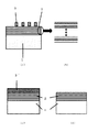
本発明の実施の形態を図を用いて説明する。図1(a)は本発明のEUV露光用マスクの実施形態の例を断面で示した説明図であり、図1(b)は、(a)の多層膜2の部分拡大図である。本発明のEUV露光用マスクは、基板上1に、露光光の高反射領域となる多層膜2を有し、前記多層膜2上に低反射領域となる吸収性薄膜のパターン3を有するEUV露光用マスクを前提とする。そして、低反射部となる吸収性薄膜は、波長150nmから300nmの紫外線に対する消衰係数が、0.2から1.0の範囲にあることを特徴とする。
【0012】
なお、ここで、吸収性薄膜のパターン3の下には、パターニングや欠陥修正の際に、高反射部となる多層膜2を保護する緩衝膜が存在することもある。さらに高反射領域となる多層膜2は、その最上層のみが「Capping Layer」と呼ばれる厚めの膜である場合もあるが、いずれも本発明の効果に影響を与えないので図1では省略する。
【0013】
また、図1(c)(d)は本発明のEUV露光用マスクブランクの実施形態の例を断面で示した説明図である。図1(c)のブランクの吸収性薄膜3’をパターニングすることにより図1(a)のマスクが得られる。図1(d)は図1(c)のブランクにおいて、吸収性薄膜3’を形成する前の形態である。
以下、図1(a)のEUV露光用マスクについて、代表して説明を行う。
【0014】
すなわち、低反射部となる吸収性薄膜は、波長150nmから300nmの紫外線に対する消衰係数が、0.2から1.0の範囲にすることで、多層膜と吸収性薄膜の反射率比は極大になる。
このような構成にすることにより、反射率比が極大となることを以下に述べる。
【0015】
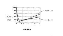
図2は消衰係数に対して、反射率比を示したグラフである。横軸は吸収性薄膜の消衰係数k、縦軸は反射率比R/R0(%)を表す。ここで、
R :吸収膜部の反射率
R0 :多層膜部の反射率
なお、吸収膜は金属性膜であるので、DUV光に対する屈折率(n)は0.8から2.5の間にほとんどの場合含まれる。また、EUV光に対する吸収性と微細加工性を確保するために、吸収膜の膜厚は500Åから1000Åが妥当である。
【0016】
図2では、屈折率をパラメタとし(0.8、2.0)、検査光波長257nm、吸収膜膜厚1000Åとして計算した場合のグラフである。同様に図3では、検査光波長257nm、吸収膜膜厚500Å、図4では、検査光波長193nm、吸収膜膜厚1000Å、図5では、検査光波長193nm、吸収膜膜厚500Åとした場合である。
【0017】
図から解るように、屈折率(n)が0.8から2.0の範囲にあるほとんどの吸収膜において、R/ROは極小値を一つ持ち、このとき反射率コントラストは極大になる。そのときkはおおむね0.2から1.0の範囲にある。この関係は波長や膜厚を変更しても成り立っている。
【0018】
また、多層膜2は2種類の膜を交互に積層し、そして2種類の膜を、Moを主成分とする膜とSiを主成分とする膜とする。これによって、界面が急峻で、屈折率差が大きく、各層対からの僅かな反射成分が干渉して強め合い、吸収がなるべく小さな多層膜とし、反射率を高めることができる。
【0019】
本発明のEUVマスクは、従来どおりのマスク作製プロセスに準拠して作製できる。すなわち、Siウェハーやガラス基板1上に、例えばMoとSiからなる多層膜を、通常のマグネトロンスパッタリング法やイオンビームスパッタリング法などにより、所望の層数の膜を積層して高反射領域2とする。その上に低反射(吸収)領域3’として、通常のマグネトロンスパッタリング法などにより薄膜を作製し、本発明のEUVハーフトーンマスク用ブランクが完成する。
【0020】
以下、通常のマスク作製プロセスに従って、薄膜のパターニングを行い、本発明のEUVハーフトーンマスクを作製する。すなわち、前記ブランク上に電子線レジストを塗布し、ベーキングを行った後、通常の電子線描画を行い、現像してレジストパターンを形成する。その後、このレジストパターンをマスクにして、低反射用2層膜のドライエッチングを行った後、レジストを剥離して、本発明のハーフトーンマスクが完成する。
【0021】
本発明によるフォトマスクを用いたパターン転写方法は、例えば、先ず被加工層を表面に形成した基板上にフォトレジスト層を設けたのち、本発明によるフォトマスクを介して反射した極限紫外線を選択的に照射する。
【0022】
次いで、現像工程において不必要な部分のフォトレジスト層を除去し、基板上にエッチングレジスト層のパターンを形成させたのち、このエッチングレジスト層のパターンをマスクとして被加工層をエッチング処理し、次いで、エッチングレジスト層のパターンを除去することにより、フォトマスクパターンに忠実なパターンを基板上に転写する方法である。
【0023】
【発明の効果】
本発明では、以上のような構成、作用をもつから、吸収膜材料が多層膜とのDUV光反射率コントラクトを大きくでき、DUV露光による欠陥検査能力を向上するEUV露光用マスクおよびそれを作製するためのブランク並びにそのマスクを用いたパターン形成方法とすることができる。
【図面の簡単な説明】
【図1】(a)本発明のEUV露光用マスクの実施形態の例を断面で示した説明図である。
(b)は、(a)の多層膜2の部分拡大図である。
(c)、(d)は、本発明のEUV露光用マスクブランクの実施形態の例を断面で示した説明図である。
【図2】消衰係数に対して、反射率比を示したグラフである。
【図3】消衰係数に対して、反射率比を示した他のグラフである。
【図4】消衰係数に対して、反射率比を示したその他のグラフである。
【図5】消衰係数に対して、反射率比を示したその他のグラフである。
【符号の説明】
1…基板
2…高反射多層膜
3…低反射薄膜パターン
3’…低反射薄膜(吸収性薄膜)[0001]
TECHNICAL FIELD OF THE INVENTION
The present invention relates to a mask for extreme ultraviolet exposure used in a photolithography process using extreme ultraviolet exposure during a semiconductor manufacturing process, a blank for producing the mask, and a pattern transfer method using the mask. Things.
[Prior art]
[0002]
The miniaturization technology of semiconductor integrated circuits is constantly progressing, and the wavelength of light used for photolithography technology for miniaturization is gradually becoming shorter. As a light source, the KrF excimer laser (wavelength 248 nm), which has been used so far, is being switched to an ArF excimer laser (wavelength 193 nm), and then the use of an F2 excimer laser (wavelength 157 nm) has been proposed. Such deep ultraviolet (DUV) has been developed.
[0003]
However, even with an F2 excimer laser, it is not easy to apply it as a lithography technique for fabricating a device having a line width of 50 nm or less in the future due to problems with an exposure machine and a resist. For this reason, research and development of EUV lithography using extreme ultraviolet (Extreme UV, hereinafter abbreviated as EUV) whose wavelength is shorter than the excimer laser beam by one digit or more (10 to 15 nm) is being promoted.
[0004]
In EUV exposure, since the wavelength is short as described above, the refractive index of a substance is almost close to a vacuum value, and the difference in light absorption between materials is small. For this reason, in the EUV region, a conventional transmissive refraction optical system cannot be assembled, and a reflection optical system is used. Therefore, the mask is also a reflection mask. A typical EUV mask that has been developed is a high-reflection region consisting of, for example, a multilayer film in which about 40 layers of two layers of Mo and Si are stacked on a Si wafer or a glass substrate, and a low-reflection region is formed thereon. The structure was such that a pattern of a metallic film was formed as a region (absorption region). The high-reflection region has a steep interface, a large difference in refractive index, and alternately stacks two types of films having as small an absorption as possible. The thickness of a pair of two adjacent layers is set to approximately one half of the exposure wavelength. About 40 pairs of two-layer films. As a result, slight reflection components from each layer pair interfere with each other and reinforce each other, so that it is possible to obtain a relatively high reflectance with respect to EUV light near normal incidence.
[0005]
[Non-patent document 1]
Ogawa, "Multilayer film for reflective mask of EUV lithography" (Optical Technology Contact, Vol. 39, No. 5, 2001, Japan Opto-Mechatronics Association) p. 292
[0006]
[Problems to be solved by the invention]
In the defect inspection of the EUV mask or the blank as described above, light reflected by DUV is used because the line width is small. What is problematic is the ratio of the reflectance of the multilayer film and the absorption film to DUV light, that is, the so-called contrast.
In the present invention, in order to improve the defect inspection capability by DUV exposure, an EUV exposure mask in which an absorption film material is defined so that the DUV light reflectance ratio with a multilayer film can be increased, a blank for producing the same, and a blank thereof Provided is a pattern forming method using a mask.
[0007]
[Means for Solving the Problems]
The invention according to
[0008]
The invention according to
[0009]
The invention according to
[0010]
The invention of claim 4 of the present invention is characterized in that the extreme ultraviolet exposure mask according to
[0011]
BEST MODE FOR CARRYING OUT THE INVENTION
An embodiment of the present invention will be described with reference to the drawings. FIG. 1A is an explanatory view showing a cross section of an embodiment of the EUV exposure mask of the present invention, and FIG. 1B is a partially enlarged view of the
[0012]
Here, a buffer film for protecting the
[0013]
FIGS. 1C and 1D are explanatory views showing a cross section of an embodiment of a mask blank for EUV exposure according to the present invention. The mask shown in FIG. 1A is obtained by patterning the blank absorbent
Hereinafter, the EUV exposure mask of FIG. 1A will be described as a representative.
[0014]
That is, by setting the extinction coefficient of ultraviolet light having a wavelength of 150 nm to 300 nm in the range of 0.2 to 1.0, the reflectance ratio between the multilayer film and the absorbing thin film is maximized. become.
It will be described below that the reflectance ratio becomes maximum by adopting such a configuration.
[0015]
FIG. 2 is a graph showing the reflectance ratio with respect to the extinction coefficient. The horizontal axis represents the extinction coefficient k of the absorptive thin film, and the vertical axis represents the reflectance ratio R / R 0 (%). here,
R: the reflectance of the absorption film portion R 0 : the reflectance of the multilayer film portion Since the absorption film is a metallic film, the refractive index (n) for DUV light is almost between 0.8 and 2.5. Case included. Further, in order to secure the absorbability to EUV light and the fine workability, the thickness of the absorbing film is appropriately from 500 ° to 1000 °.
[0016]
FIG. 2 is a graph in which the refractive index is a parameter (0.8, 2.0), the inspection light wavelength is 257 nm, and the absorption film thickness is 1000 °. Similarly, FIG. 3 shows the case where the inspection light wavelength is 257 nm and the absorption film thickness is 500 °, FIG. 4 shows the case where the inspection light wavelength is 193 nm and the absorption film thickness is 1000 °, and FIG. is there.
[0017]
As can be seen, in most of the absorbing films having a refractive index (n) in the range of 0.8 to 2.0, R / R O has one minimum value, and the reflectance contrast becomes maximum at this time. . Then k is generally in the range of 0.2 to 1.0. This relationship holds even when the wavelength or the film thickness is changed.
[0018]
The
[0019]
The EUV mask of the present invention can be manufactured according to a conventional mask manufacturing process. That is, a high-
[0020]
Hereinafter, the thin film is patterned according to a normal mask manufacturing process to manufacture the EUV halftone mask of the present invention. That is, after applying an electron beam resist on the blank and performing baking, normal electron beam drawing is performed and developed to form a resist pattern. Thereafter, using this resist pattern as a mask, the low-reflection two-layer film is dry-etched, and then the resist is peeled off to complete the halftone mask of the present invention.
[0021]
The pattern transfer method using the photomask according to the present invention includes, for example, first providing a photoresist layer on a substrate on which a layer to be processed is formed on the surface, and then selectively exposing the ultimate ultraviolet light reflected through the photomask according to the present invention. Irradiation.
[0022]
Next, in the developing step, unnecessary portions of the photoresist layer are removed, and after forming a pattern of the etching resist layer on the substrate, the layer to be processed is etched using the pattern of the etching resist layer as a mask, This is a method of transferring a pattern faithful to a photomask pattern onto a substrate by removing the pattern of the etching resist layer.
[0023]
【The invention's effect】
In the present invention, because of the above configuration and function, the EUV exposure mask and the manufacturing of the EUV exposure mask which can increase the DUV light reflectance contract between the absorbing film material and the multilayer film and improve the defect inspection capability by DUV exposure And a pattern forming method using the mask.
[Brief description of the drawings]
FIG. 1A is an explanatory view showing a cross section of an example of an embodiment of an EUV exposure mask of the present invention.
(B) is a partially enlarged view of the
(C), (d) is explanatory drawing which showed the example of embodiment of the mask blank for EUV exposure of this invention in cross section.
FIG. 2 is a graph showing a reflectance ratio with respect to an extinction coefficient.
FIG. 3 is another graph showing a reflectance ratio with respect to an extinction coefficient.
FIG. 4 is another graph showing a reflectance ratio with respect to an extinction coefficient.
FIG. 5 is another graph showing a reflectance ratio with respect to an extinction coefficient.
[Explanation of symbols]
DESCRIPTION OF
Claims (4)
Priority Applications (1)
| Application Number | Priority Date | Filing Date | Title |
|---|---|---|---|
| JP2003050634A JP4529359B2 (en) | 2003-02-27 | 2003-02-27 | Ultraviolet exposure mask, blank and pattern transfer method |
Applications Claiming Priority (1)
| Application Number | Priority Date | Filing Date | Title |
|---|---|---|---|
| JP2003050634A JP4529359B2 (en) | 2003-02-27 | 2003-02-27 | Ultraviolet exposure mask, blank and pattern transfer method |
Publications (2)
| Publication Number | Publication Date |
|---|---|
| JP2004260050A true JP2004260050A (en) | 2004-09-16 |
| JP4529359B2 JP4529359B2 (en) | 2010-08-25 |
Family
ID=33115994
Family Applications (1)
| Application Number | Title | Priority Date | Filing Date |
|---|---|---|---|
| JP2003050634A Expired - Fee Related JP4529359B2 (en) | 2003-02-27 | 2003-02-27 | Ultraviolet exposure mask, blank and pattern transfer method |
Country Status (1)
| Country | Link |
|---|---|
| JP (1) | JP4529359B2 (en) |
Cited By (7)
| Publication number | Priority date | Publication date | Assignee | Title |
|---|---|---|---|---|
| JP2006228767A (en) * | 2005-02-15 | 2006-08-31 | Toppan Printing Co Ltd | Mask for extreme ultraviolet ray exposure, mask blank, and exposure method |
| JP2007273651A (en) * | 2006-03-31 | 2007-10-18 | Toppan Printing Co Ltd | Mask blank for extreme ultraviolet ray exposure, mask for extreme ultraviolet ray exposure, and pattern transfer method |
| JP2007273652A (en) * | 2006-03-31 | 2007-10-18 | Toppan Printing Co Ltd | Mask blank for extreme ultraviolet ray exposure, mask for extreme ultraviolet ray exposure, and pattern transfer method |
| JPWO2006062099A1 (en) * | 2004-12-10 | 2008-06-12 | 凸版印刷株式会社 | Reflective photomask blank, reflective photomask, and semiconductor device manufacturing method using the same |
| JP2008277397A (en) * | 2007-04-26 | 2008-11-13 | Toppan Printing Co Ltd | Reflection type photomask blank and reflection type photomask, and method of manufacturing semiconductor device |
| JP2011002528A (en) * | 2009-06-17 | 2011-01-06 | Toshiba Corp | Photomask inspection method |
| CN106575076A (en) * | 2014-08-13 | 2017-04-19 | 卡尔蔡司Smt有限责任公司 | Mask for euv lithography, euv lithography apparatus and method for determining a contrast proportion caused by duv radiation |
Citations (2)
| Publication number | Priority date | Publication date | Assignee | Title |
|---|---|---|---|---|
| JP2002246299A (en) * | 2001-02-20 | 2002-08-30 | Oki Electric Ind Co Ltd | Reflecting type exposure mask, its manufacturing method and semiconductor element |
| JP2004006798A (en) * | 2002-04-11 | 2004-01-08 | Hoya Corp | Reflective mask blank, reflective mask, method for manufacturing the same and method for manufacturing semiconductor |
-
2003
- 2003-02-27 JP JP2003050634A patent/JP4529359B2/en not_active Expired - Fee Related
Patent Citations (2)
| Publication number | Priority date | Publication date | Assignee | Title |
|---|---|---|---|---|
| JP2002246299A (en) * | 2001-02-20 | 2002-08-30 | Oki Electric Ind Co Ltd | Reflecting type exposure mask, its manufacturing method and semiconductor element |
| JP2004006798A (en) * | 2002-04-11 | 2004-01-08 | Hoya Corp | Reflective mask blank, reflective mask, method for manufacturing the same and method for manufacturing semiconductor |
Cited By (10)
| Publication number | Priority date | Publication date | Assignee | Title |
|---|---|---|---|---|
| JPWO2006062099A1 (en) * | 2004-12-10 | 2008-06-12 | 凸版印刷株式会社 | Reflective photomask blank, reflective photomask, and semiconductor device manufacturing method using the same |
| US7838177B2 (en) | 2004-12-10 | 2010-11-23 | Toppan Printing Co., Ltd. | Reflection type photomask blank, reflection type photomask, and method of manufacturing semiconductor device using the same |
| JP5003159B2 (en) * | 2004-12-10 | 2012-08-15 | 凸版印刷株式会社 | Reflective photomask blank, reflective photomask, and semiconductor device manufacturing method using the same |
| JP2006228767A (en) * | 2005-02-15 | 2006-08-31 | Toppan Printing Co Ltd | Mask for extreme ultraviolet ray exposure, mask blank, and exposure method |
| JP2007273651A (en) * | 2006-03-31 | 2007-10-18 | Toppan Printing Co Ltd | Mask blank for extreme ultraviolet ray exposure, mask for extreme ultraviolet ray exposure, and pattern transfer method |
| JP2007273652A (en) * | 2006-03-31 | 2007-10-18 | Toppan Printing Co Ltd | Mask blank for extreme ultraviolet ray exposure, mask for extreme ultraviolet ray exposure, and pattern transfer method |
| JP2008277397A (en) * | 2007-04-26 | 2008-11-13 | Toppan Printing Co Ltd | Reflection type photomask blank and reflection type photomask, and method of manufacturing semiconductor device |
| JP2011002528A (en) * | 2009-06-17 | 2011-01-06 | Toshiba Corp | Photomask inspection method |
| CN106575076A (en) * | 2014-08-13 | 2017-04-19 | 卡尔蔡司Smt有限责任公司 | Mask for euv lithography, euv lithography apparatus and method for determining a contrast proportion caused by duv radiation |
| CN106575076B (en) * | 2014-08-13 | 2021-07-13 | 卡尔蔡司Smt有限责任公司 | Mask for EUV lithography, EUV lithography apparatus and method for determining a contrast ratio caused by DUV radiation |
Also Published As
| Publication number | Publication date |
|---|---|
| JP4529359B2 (en) | 2010-08-25 |
Similar Documents
| Publication | Publication Date | Title |
|---|---|---|
| JP2009099931A (en) | Reflective photomask blank and manufacturing method thereof, reflective photomask and manufacturing method thereof, and manufacturing method of semiconductor device | |
| JP2004207593A (en) | Mask for extreme ultra-violet exposure, blank, and method for pattern transfer | |
| KR101076886B1 (en) | Mask for EUV lithography and method for exposure using the same | |
| JP2924791B2 (en) | Photomask and method of manufacturing photomask | |
| KR100940270B1 (en) | Extreme UltraViolet mask and method for fabricating the same | |
| JPH1083065A (en) | Phase shift mask and its production | |
| JP4529359B2 (en) | Ultraviolet exposure mask, blank and pattern transfer method | |
| JP4923923B2 (en) | Extreme ultraviolet exposure mask and semiconductor integrated circuit manufacturing method using the same | |
| JP2008288361A (en) | Reflection type photo mask blank, manufacturing method thereof, reflection type photo mask blank, and manufacturing method of semiconductor device | |
| JP2011249391A (en) | Reflective photomask and manufacturing method thereof, and pattern formation method | |
| JP4622504B2 (en) | Mask blank for extreme ultraviolet exposure, mask and pattern transfer method | |
| JP4483355B2 (en) | Ultraviolet exposure mask blank, mask and transfer method | |
| JP4501347B2 (en) | Ultraviolet exposure mask, blank and pattern transfer method | |
| US8697318B2 (en) | Method of forming photomasks and photomasks formed by the same | |
| JP4613499B2 (en) | Ultraviolet exposure mask, blank, mask manufacturing method, and pattern transfer method | |
| JP4605284B2 (en) | Extreme ultraviolet exposure mask, extreme ultraviolet exposure mask blank, and pattern transfer method | |
| US8673521B2 (en) | Blank substrates for extreme ultra violet photo masks and methods of fabricating an extreme ultra violet photo mask using the same | |
| JP4300930B2 (en) | Ultraviolet exposure mask, blank and pattern transfer method | |
| JP4273776B2 (en) | Extreme UV exposure mask | |
| JP4977794B2 (en) | Pattern transfer method and photomask | |
| KR100966980B1 (en) | Method for compensating semiconductor CD | |
| JP4923922B2 (en) | Extreme ultraviolet exposure mask, manufacturing method thereof, and semiconductor integrated circuit manufacturing method using the same | |
| KR20210155863A (en) | Phase shift mask for extreme ultraviolet lithography and method of forming a semiconductor device using the same | |
| KR100824904B1 (en) | Reflective Mask with Notched Assist Feature | |
| KR20110089759A (en) | Extreme ultra violet mask and method of manufacturing the same |
Legal Events
| Date | Code | Title | Description |
|---|---|---|---|
| A621 | Written request for application examination |
Free format text: JAPANESE INTERMEDIATE CODE: A621 Effective date: 20060125 |
|
| A977 | Report on retrieval |
Free format text: JAPANESE INTERMEDIATE CODE: A971007 Effective date: 20080815 |
|
| A131 | Notification of reasons for refusal |
Free format text: JAPANESE INTERMEDIATE CODE: A131 Effective date: 20080902 |
|
| A521 | Written amendment |
Free format text: JAPANESE INTERMEDIATE CODE: A523 Effective date: 20081021 |
|
| A131 | Notification of reasons for refusal |
Free format text: JAPANESE INTERMEDIATE CODE: A131 Effective date: 20090602 |
|
| A521 | Written amendment |
Free format text: JAPANESE INTERMEDIATE CODE: A523 Effective date: 20090728 |
|
| A131 | Notification of reasons for refusal |
Free format text: JAPANESE INTERMEDIATE CODE: A131 Effective date: 20090901 |
|
| TRDD | Decision of grant or rejection written | ||
| A01 | Written decision to grant a patent or to grant a registration (utility model) |
Free format text: JAPANESE INTERMEDIATE CODE: A01 Effective date: 20100518 |
|
| A01 | Written decision to grant a patent or to grant a registration (utility model) |
Free format text: JAPANESE INTERMEDIATE CODE: A01 |
|
| A61 | First payment of annual fees (during grant procedure) |
Free format text: JAPANESE INTERMEDIATE CODE: A61 Effective date: 20100531 |
|
| R150 | Certificate of patent or registration of utility model |
Free format text: JAPANESE INTERMEDIATE CODE: R150 |
|
| FPAY | Renewal fee payment (event date is renewal date of database) |
Free format text: PAYMENT UNTIL: 20130618 Year of fee payment: 3 |
|
| LAPS | Cancellation because of no payment of annual fees |