JP2004259752A - Electronic device and method of manufacturing electronic device - Google Patents
Electronic device and method of manufacturing electronic device Download PDFInfo
- Publication number
- JP2004259752A JP2004259752A JP2003045967A JP2003045967A JP2004259752A JP 2004259752 A JP2004259752 A JP 2004259752A JP 2003045967 A JP2003045967 A JP 2003045967A JP 2003045967 A JP2003045967 A JP 2003045967A JP 2004259752 A JP2004259752 A JP 2004259752A
- Authority
- JP
- Japan
- Prior art keywords
- wiring
- electronic device
- superconducting
- pressing
- sheet
- Prior art date
- Legal status (The legal status is an assumption and is not a legal conclusion. Google has not performed a legal analysis and makes no representation as to the accuracy of the status listed.)
- Pending
Links
Images

Landscapes
- Waveguides (AREA)
- Superconductor Devices And Manufacturing Methods Thereof (AREA)
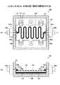
- Containers, Films, And Cooling For Superconductive Devices (AREA)
- Control Of Motors That Do Not Use Commutators (AREA)
Abstract
【課題】電子装置を小型化し、当該電子装置の冷却装置の負荷を軽減する。
【解決手段】誘電体基板12に超伝導配線13が形成されると共に、反対側に位置する面に超伝導接地膜18が配設された電子素子と、該電子素子を装着する構成とされており、装着状態において前記超伝導接地膜18と接続される接地部と、前記超伝導配線13に接続される中心導体15a,15bと、前記電子素子を前記接地部に向け押圧する押圧手段とを有してなる金属筐体11とを具備する電子装置であって、前記押圧手段は、前記中心導体15a,15bに弾性を持たせ、該中心導体15a,15bの弾性力により前記電子素子を押圧することにより、前記電子素子を前記接地部に向け押圧する構成であることを特徴とする電子装置。
【選択図】 図2An electronic device is reduced in size and a load on a cooling device of the electronic device is reduced.
An electronic device having a superconducting wiring formed on a dielectric substrate and a superconducting ground film disposed on a surface located on the opposite side, and a structure for mounting the electronic device. And a grounding portion connected to the superconducting grounding film 18 in the mounted state, central conductors 15a and 15b connected to the superconducting wiring 13, and pressing means for pressing the electronic element toward the grounding portion. An electronic device comprising: a metal casing 11 having the elasticity; and the pressing means presses the electronic element by elasticity of the center conductors 15a and 15b. The electronic device is configured to press the electronic element toward the ground portion.
[Selection] Fig. 2
Description
【0001】
【発明の属する技術分野】
本発明は、電子装置に係り、特に高周波デバイスに適用して好適な電子装置に関する。
【0002】
近年、無線通信やインターネットなどの爆発的な普及発展に伴い、高速・大容量の伝送技術が不可欠となってきている。そのためには、高周波の信号を低損失で、さらに歪の少ない状態で伝送する高品質の伝送線路が必要である。
【0003】
前記したような高品質の伝送線路として、例えば超伝導体を適用することが考えられる。超伝導体は、通常の電気的良導体と比較して高周波領域において表面抵抗が非常に小さく、位相分散も極めて低い。したがって、例えば超伝導体を伝送線に用いたマイクロスプリット伝送線路は、次世代の伝送技術として非常に有望であり、特に超高速のデジタル回路や、SFQ(Single Flux Quantum、単一量子磁束デバイス)を実装する基板の配線などへ適用することが期待されている。
【0004】
しかし、前記したような超伝導体を用いる場合、当該超伝導体を冷却しなければならないため、冷却手段の負担が大きいという問題がある。例えば、酸化物超伝導体の発見によって、冷却温度の条件は大幅に緩和されたものの、依然として液体窒素の沸点付近までは冷却する必要がある。そのため、実用を考慮した場合には前記したような冷却の負担を軽減することが重要である。
【0005】
【従来の技術】
従来用いられている電子装置の例として、図1(A)および(B)に、従来用いられている超伝導マイクロスプリット伝送線路を用いて遅延回路を形成した高周波デバイス100の基本構造を示す。図1(A)は平面図であり、図1(B)は、図1(A)に示したX−X線での断面図である。
【0006】
図1(A)を参照するに、高周波デバイス100の概要は、高周波電磁シールドが可能な金属筐体101に、超伝導配線103が形成された誘電体基板102が収納された構造となっている。前記金属筐体101には、それぞれ中心導体105aおよび105bを有する同軸コネクタ104aおよび104bが取り付けられている。前記中心導体105aおよびb105bは、それぞれ前記誘電体基板上の前記超伝導配線103の一部を覆うように形成された配線電極106aおよび106bに電気的に接触している。さらに、前記中心導体105aおよび105bと、前記配線電極106aおよび106bは、それぞれハンダ107aおよび107bにて固定されて、電気抵抗が低減されている。このようにして、同軸コネクタ104aから同軸コネクタ104bへの伝送線路である遅延回路が形成されている。
【0007】
また、前記金属筐体101には、ネジ受け111が設けられており、前記誘電体基板102に取り付けられた板バネ112の穴を通してネジ113が前記ネジ受け111に固定されている。これは、前記板バネ112の弾性力で、前記板バネ112が取り付けられた前記誘電体基板102を、前記金属筐体101に押し付けるためのものである。詳細については後述する。
【0008】
次に、図1(B)を参照する。ただし図中、先に説明した部分には同一の参照符号を付し、説明を省略する。
【0009】
前記誘電体基板102の、前記超伝導配線103が形成されている面の反対の面には、略全面に超伝導接地膜108が形成されており、さらに当該超伝導接地膜108の膜に重ねて接地電極109が形成されている。前記超伝導接地電極109と前記金属筐体101の間にはInシート110が挿入されている。前記したように、前記板バネ112の弾性力によって前記誘電体基板102が前記金属筐体に押し付けられる。そのため、前記Inシート110が変形して、当該Inシート110と、前記接地電極109および前記金属筐体101の接触面積が増加する。その結果、前記Inシート110を介して前記接地電極109と前記金属筐体101の電気抵抗が低減すると共に、熱抵抗も低減させることができる。
【0010】
【特許文献1】
特開2001−35598号公報
【0011】
【発明が解決しようとする課題】
ところで、前記した高周波デバイス100を実際に動作させるためには、冷却する必要があり、冷凍機や断熱用の真空容器といった大規模な設備を付加する必要が有る。そのため、前記高周波デバイス100を小型化することが可能であれば、冷凍機の熱付加を小さくすることができ、さらには断熱用の真空装置も小型化することで設備全体を小型化することが可能となり、さらにはコストを削減することが可能である。
【0012】
しかし、前記したように、高周波デバイス100は、前記誘電体基板102を前記金属筐体101に押し付けるための前記板バネ112、ネジ受け111などの部品を設置する必要があり、前記高周波デバイス100を小型化する際の問題となっていた。このため、高周波デバイス100を用いた電子装置を小型化することには限界があり、そのために前記電子装置を冷却する冷凍設備の小型化することが困難となり、冷凍設備のコスト削減の問題となっていた。
【0013】
そこで、本発明では前記の課題を解決した新規で有用な電子装置を提供することを課題としている。
【0014】
本発明の具体的な課題は、超伝導体を用いた高周波デバイスを含む電子装置を小型化することにより省スペース化を実現し、かつ当該電子装置を冷却する冷却設備の熱負荷を低減することである。
【0015】
【課題を解決するための手段】
本発明では上記の課題を解決するために、基板の第1の面に第1の配線が形成されると共に、第1の面の反対側に位置する第2の面に第2の配線が配設された電子素子と、該電子素子を装着する構成とされており、装着状態において前記第2の配線と接続される接地部と、前記第1の配線に接続される接続配線と、前記電子素子を前記電極に向け押圧する押圧手段とを有してなる筐体とを具備する電子装置であって、前記押圧手段は、前記接続配線に弾性を持たせ、該接続配線の弾性力により前記電子素子を押圧することにより、前記電子素子を前記接地部に向け押圧する構成であることを特徴とする電子装置により、また、前記第1の配線および前記第2の配線は超伝導媒体よりなることを特徴とする電子装置により、解決する。
【0016】
本発明によれば、前記筐体に配設された電子装置において、当該電子装置の回路の一部を形成する前記接続配線に、当該接続配線の弾性力により前記電子素子を前記筐体の前記接地部に押圧する機能を付加した。その結果、従来必要であった前記電子素子を押し付けるための構造が不用となり、前記筐体を小型化して電子装置を小型化することが可能となり、省スペースが実現し、また、そのために超伝導媒体を用いた配線を冷却する冷却設備の熱負荷を軽減することが可能となる。
【0017】
本発明では、上記の課題を、基板の第1の面に第1の配線が形成されると共に、第1の面の反対側に位置する第2の面に第2の配線が配設された電子素子を、接地部と接続配線を有する筐体に装着する電子装置の製造方法であって、前記電子素子を前記筐体に載置して前記第2の配線と前記接地部を接続する工程と、前記接続配線に前記第2の配線を接続する工程と、前記接続配線の弾性力により、前記電子素子を押圧することにより、前記電子素子を前記接地部に向け押圧する工程とを有することを特徴とする電子装置の製造方法により、解決する。
【0018】
本発明によれば、前記筐体に配設する電子装置の製造方法において、当該電子装置の回路の一部を形成する前記接続配線に、当該接続配線の弾性力により前記電子素子を前記筐体の前記接地部に押圧する工程を設けた。その結果、従来必要であった前記電子素子を押し付けるための構造が不用となり、前記筐体を小型化して電子装置を小型化することが可能となり、省スペースが実現する。
【0019】
そのため、例えば、電子装置内に超伝導媒体を用いた場合、当該超伝導媒体を冷却する冷却設備への負担を軽減することが可能となる。
【0020】
【発明の実施の形態】
次に、本発明の実施の形態について、図面に基づき以下に説明する。
[第1実施例]
図2(A)および(B)は、本発明による電子装置の例である高周波デバイス10の基本構造図である。図2(A)は平面図を示し、図2(G)は、当該平面図中に示したX−X面による断面図を示す。
【0021】
図2(A)を参照するに、高周波デバイス10の概要は、高周波電磁シールドが可能な、例えばAl合金からなる金属筐体11に、超伝導配線13が形成された誘電体基板12が収納された構造となっている。本実施の形態の場合の前記誘電体基板13はおよそ40mm×20mm程度の大きさである。前記金属筐体11には、それぞれ中心導体15a、15bを有する同軸コネクタ14a、14bが取り付けられている。前記中心導体15aおよびb15bは、それぞれ前記誘電体基板上の前記超伝導配線13の一部を覆うように形成された配線電極16aおよび16bに電気的に接触している。さらに、前記中心導体15aおよび15bと、前記配線電極16aおよび16bは、それぞれハンダ17aおよび17bにて固定されて、電気抵抗が低減されている。このようにして、同軸コネクタ14aから同軸コネクタ14bへの伝送線路である遅延回路が形成されている。
【0022】
次に、図2(B)を参照する。ただし図中、先に説明した部分には同一の参照符号を付し、説明を省略する。
【0023】
前記誘電体基板12の、前記超伝導配線13が形成されている面の反対の面には、略全面に超伝導接地膜18が形成されており、さらに当該超伝導接地膜18を覆うように接地電極19が形成されている。前記超伝導接地電極19と前記金属筐体11の間にはInシート20が挿入されている。
【0024】
本実施の形態においては、前記同軸コネクタ14aおよび14bから、前記中心導体15aおよび15bが、前記誘電体基板12に向かって斜めに取り付けられており、前記誘電体基板12が装着された時点で前記同軸コネクタ15aおよび15bの弾性力が、当該誘電体基板12を押し付ける方向に働く構造としている。また、前記中心導体15aおよび15bは、弾性力が働き、かつ当該弾性力の反力に耐えうるように直径が太いものを使用している。このようにして、前記前記中心導体15aおよび15bの弾性力によって前記誘電体基板12が前記金属筐体11に押し付けられている。そのため、前記Inシート20が変形して、当該Inシート20と、前記接地電極19および前記金属筐体11の接触面積が増加する。その結果、前記Inシート20を介して前記接地電極19と前記金属筐体11の電気抵抗が低減すると共に、熱抵抗も低減させることができる。その結果、前記接地電極19に接する前記超伝導接地面18の電位とアース電位である前記金属筐体11の電位を同じにすることができ、損失の少ない高周波デバイスを形成することができる。また、前記熱抵抗を低減することができるため、例えば前記高周波デバイス10を冷却する際に、前記超伝導電線13および前記超伝導接地膜18の冷却効率を上げることができる。
【0025】
また、例えば図1(A)に示した従来例の場合、上記したような接触面積の増加の効果を得るために、前記ネジ受け111、前記板バネ112、前記板ネジ113などの部品を設ける必要が有り、その結果高周波デバイスの小型化に限界があった。しかし、図2(A)および(B)に示した本実施例においては、高周波の伝送経路の一部である前記中心導体15aおよび15bに、前記誘電体基板12を前記金属筐体11に押し付ける機能をさらに付加する構造としたために、前記高周波デバイス10の小型化が可能となり、設置面積を従来品の約80%に押さえることができる。また、実際に前記高周波デバイス10を使用する際は、前記高周波デバイス10を冷却する必要がある。その場合、本実施例による高周波デバイス10は、小型化されているため、冷却の際の負担を小さくすることが可能である。
【0026】
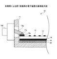
図3は、図2(B)にAで示した領域の拡大図である。ただし図中、先に説明した部分には同一の参照符号を付し、一部説明を省略する。
【0027】
前記金属筐体11は、例えばAl合金からなるが、高周波電磁シールドが可能であれば他の材質を用いても良く、例えばAl、Cu、Au、Agなどを用いることが可能である。また、前記誘電体基板12は本実施例においてはMgOの単結晶の基板を用いているが、誘電損失が少ない材料であればよく、例えばAl2O3、LaAlO3などを用いてもよい。前記超伝導配線13および前記超伝導接地膜18は、ペロブスカイト酸化物であるYBCO(YBa2Cu3O7− δ(0<δ<0.3))からなるが、これは他のペロブスカイト酸化物、さらに他の酸化物超伝導体を用いてもよく、例えば、Bi−Sr−Ca−Cu−O系(Bi2Sr2Can−1CunO2n+4)、もしくはTl−Ba−Ca−Cu−O系などの材料を用いてもよい。前記配線電極配線電極16a、16bおよび接地電極19には、Ag/Pd/Cr構造を用いている。
【0028】
また、前記中心導体15aおよび15bは弾性力によって、前記誘電体基板12を前記金属筐体11に略20gの力で押し付ける。この押し付ける力が弱いと、前記Inシート20の変形が十分でなく、当該Inシート20と、前記接地電極19および前記金属筐体11の接触面積の増加量が少なく、十分な効果が得られない。また、押し付ける力が強すぎると前記誘電体基板12が破損してしまう。そのため、本実施例においては、前記誘電体基板12を5g〜70g程度の力で押し付けることが必要である。さらに、前記Inシート20は、本実施例においては厚さが0.1mmのものを使用している。前記Inシートの厚さが薄すぎると前記したように、前記Inシート20の変形による効果が十分に得られず、また厚すぎると後述する加熱工程において前記Inシート20の熱膨張により、前記誘電体基板12が破損してしまう恐れがあるため、前記Inシート20の厚さは、0.05〜0.5mmのものを使用する必要がある。
【0029】
また、前記中心導体15aおよび15bは押し付け力に耐えられる十分な強度を持つと共に弾性力があり、さらには高周波の伝送経路の一部であるため、電気抵抗値が低い材質を用いる必要がある。本実施例では、Cuを用いているが、他にも例えば、Be−Cu、りん青銅などを使用しても、本実施例と同様の効果を得ることができる。
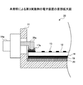
【0030】
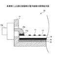
また、図3に示した前記中心導体15aは、次に図4〜6示すように変更することが可能である。
[第2実施例]
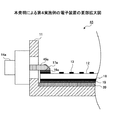
図4は、図3で示した第1実施例の電子装置である高周波デバイス10の変形例である。ただし図中、先に説明した部分には同一の参照符号を付し、説明を省略する。
【0031】
図4を参照するに、本実施例の高周波デバイス25においては、中心導体25aが前記コネクタ14a側から前記配線電極16aに向かって曲線状になっておる。具体的には、前記中心導体25aが、前記コネクタ14a側から離れるに従い前記誘電体基板12にづいていく曲線状となっている。本実施例においても、前記中心導体25aによって前記誘電体基板12を前記金属筐体11に押し付けることにより、第1実施例に前記した場合と同様の効果を得ることができる。すなわち、前記Inシート20が変形して、当該Inシート20と、前記接地電極19および前記金属筐体11の接触面積が増加する。その結果、前記Inシート20を介して前記接地電極19と前記金属筐体11の電気抵抗が低減すると共に、熱抵抗も低減させることができる。その結果、前記接地電極19に接する前記超伝導接地面18の電位とアース電位である前記金属筐体11の電位を同じにすることができ、損失の少ない高周波デバイスを形成することができる。また、前記熱抵抗を低減することができるため、例えば前記高周波デバイス10を冷却する際に、前記超伝導電線13および前記超伝導接地膜18の冷却効率を上げることができる。
[第3実施例]
図5は、図3で示した電子装置である高周波デバイス10の別の変形例である。ただし図中、先に説明した部分には同一の参照符号を付し、説明を省略する。
【0032】
図5を参照するに、本実施例の高周波デバイス35においては、中心導体35aが前記コネクタ14a側から前記配線電極16aに向かって折れ曲がっている。具体的には、前記中心導体35aは、前記誘電体基板12に略平行な部分と、前記誘電体基板12に略垂直な部分を有する。本実施例においても、前記中心導体35aによって前記誘電体基板12を前記金属筐体11に押し付けることにより、第1実施例に前記した場合と同様の効果を得ることができる。すなわち、前記Inシート20が変形して、当該Inシート20と、前記接地電極19および前記金属筐体11の接触面積が増加する。その結果、前記Inシート20を介して前記接地電極19と前記金属筐体11の電気抵抗が低減すると共に、熱抵抗も低減させることができる。その結果、前記接地電極19に接する前記超伝導接地面18の電位とアース電位である前記金属筐体11の電位を同じにすることができ、損失の少ない高周波デバイスを形成することができる。また、前記熱抵抗を低減することができるため、例えば前記高周波デバイス10を冷却する際に、前記超伝導電線13および前記超伝導接地膜18の冷却効率を上げることができる。
[第4実施例]
図6は、図3で示した電子装置である高周波デバイス10のさらに別の変形例である。ただし図中、先に説明した部分には同一の参照符号を付し、説明を省略する。
【0033】
図6を参照するに、本実施例においては、中心導体45aが前記コネクタ14a側から前記配線電極16aに接触するまで、前記誘電体基板12と略水平な構造となっている。第1実施例においては前記中心導体15aが、前記コネクタ14a側から前記配線電極16aに向かって斜めの構造、すなわち前記誘電体基板12と非平行な構造となっていた。しかし、前記中心導体45aは、押し付け力に耐えられる十分な強度を持つと共に弾性力があり、さらには高周波の伝送経路の一部であるため、抵抗値が低いという条件を満たす。具体的には、前記中心導体45aが前記誘電体基板12と略平行であるのは、当該中心導体45aが弾性変形した後の形であり、例えば実施例1に示した場合において、前記中心導体15aの弾性変形が著しい場合である。すなわち、当該条件を満たす範囲内において、中心導体は様々にその形状を変更することが可能である。そのため、本実施例においても、前記中心導体45aによって前記誘電体基板12を前記金属筐体11に押し付けることにより、第1実施例に前記した場合と同様の効果を得ることができる。すなわち、前記Inシート20が変形して、当該Inシート20と、前記接地電極19および前記金属筐体11の接触面積が増加する。その結果、前記Inシート20を介して前記接地電極19と前記金属筐体11の電気抵抗が低減すると共に、熱抵抗も低減させることができる。その結果、前記接地電極19に接する前記超伝導接地面18の電位とアース電位である前記金属筐体11の電位を同じにすることができ、損失の少ない高周波デバイスを形成することができる。また、前記熱抵抗を低減することができるため、例えば前記高周波デバイス10を冷却する際に、前記超伝導電線13および前記超伝導接地膜18の冷却効率を上げることができる。
[第5実施例]
次に、本発明による電子装置である高周波デバイスの製造方法について図面に基づき、手順をおって説明する。
【0034】
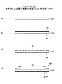
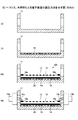
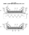
図7(A)〜(D)、図8(E)〜(H)、図9(I)〜(J)は、本発明による高周波デバイスの製造方法のフローを示したものである。ただし図中、先に説明した部分には同一の参照符号を付し、一部説明を省略する。
【0035】
まず、図7(A)を参照するに、高周波デバイスを形成するため、例えば2インチのウェハから切り出したMgOの単結晶からなる誘電体基板12を用意する。
【0036】
次に、図7(B)において、前記誘電体基板12の第1の側に、超伝導配線を形成するため、例えばスパッタリング法により、YBCOからなる超伝導膜13’を形成する。また、前記YBCOは、他に蒸着法、電子線エピタキシーなどのエピタキシー法、エキシマレーザによるPLD法などによっても形成することができる。また、同様にして前記誘電体基板12の前記第1の側の反対側である第2の側に、YBCOからなる超伝導接地膜18を形成する。
【0037】
次に、図7(C)において、フォトリソグラフィー法によって、前記超伝導膜13’に、線幅0.5mmのミアンダ上のパターニングを施して、超伝導配線13を形成する。
【0038】
次に、図7(D)において、まず前記誘電体基板12の第1の側において、メタルマスクを用いて、ミアンダパターンの一部を覆うように、真空蒸着法を用いてAg/Pd/Crからなる配線電極16aおよび16bを形成する。同様に、前記超伝導接地膜18の略全面に、真空蒸着法でAg/Pd/Crからなる接地電極19を形成する。
【0039】
ここで、前記誘電体基板12、前記超伝導配線13、前記配線電極16a,16bおよび接地電極19からなる配線板10Aが完成する。次に前記配線板10Aを、金属筐体に設置するため、次に当該金属筐体について説明する。
【0040】
図8(E)は前記配線板10Aを設置するための金属筐体11の断面図である。
【0041】
図8(F)において、前記金属筐体11に、Inシート20を設置する。また、前記Inシート20は、第1実施例の図3の説明で前記したように、厚さが0.05〜0.5mmのものを用いる必要があり、本実施例の場合は厚さが0.1mmのものを用いている。
【0042】
次に、図8(G)において、前記Inシート20が設置された前記金属筐体11に、図7(A)〜(D)の工程で形成した前記配線板10Aを設置する。その際に、前記配線板10Aの前記接地電極19と、前記金属筐体11が、前記Inシート20を介して接触するようにする。
【0043】
次に、図8(H)において、それぞれ中心導体15aおよび15bを有する同軸コネクタ14aおよび14bを前記金属筐体11に取り付ける。このとき、前記中心導体15aおよび15bがそれぞれ前記配線電極16aおよび16bに接触して電気的に接続する構成とする。このようにして、前記同軸コネクタ14aから順に前記中心導体15a、前記配線電極16a、前記超伝導配線13、前記配線電極16b、前記中心導体15bおよび前記同軸コネクタ14bへの高周波の伝送経路が完成する。
【0044】
また、第1実施例の説明で前記したように、前記中心導体15aおよび15bの弾性力によって前記誘電体基板12が前記金属筐体に略20gの力で押し付けられている。そのため、前記Inシート20が変形して、当該Inシート20と、前記接地電極19および前記金属筐体11の接触面積が増加する。その結果、前記Inシート20を介して前記接地電極19と前記金属筐体11の電気抵抗が低減すると共に、熱抵抗も低減させることができる。その結果、前記接地電極19に接する前記超伝導接地面18の電位とアース電位である前記金属筐体11の電位を同じにすることができ、損失の少ない高周波デバイスを形成することができる。また、前記熱抵抗を低減することができるため、例えば前記高周波デバイス10を冷却する際に、前記超伝導電線13および前記超伝導接地膜18の冷却効率を上げることができる。
【0045】
次に、図9(I)において、前記配線板10Aを保持する前記金属筐体11を加熱手段21に載置して、前記加熱手段21により120℃で加熱した。この際に、融点が157℃である前記Inシート20が柔らかくなり、当該Inシート20が前記金属筐体11および前記接地電極19とよく馴染んで接触面積が増加する。その結果図8(H)の説明で前記したような、前記Inシート20と、前記接地電極19および前記金属筐体11の境界面の電気抵抗が低減すると共に、当該境界面の熱抵抗を低減させる効果が増大する。また、このように加熱によってInシートを馴染ませる工程を設けることで、必要とされる中心電極による押し付け力を小さくする効果も奏する。
【0046】
次に、図9(J)において、前記中心導体15aおよび15bと、前記配線電極16aおよび16bを、こて先温度略400℃のハンダごてを用いて、それぞれハンダ17aおよび17bで固定して、高周波デバイス10が完成する。
【0047】
本実施例における高周波デバイス10の場合、高周波の伝送経路の一部である前記中心導体15aおよび15bに、前記誘電体基板12を前記金属筐体11に押し付ける機能をさらにもたせる構造としたために、前記高周波デバイス10の小型化が可能となった。また、実際に前記高周波デバイス10を使用する際は、前記高周波デバイス10を冷却する必要がある。その場合、本実施例による高周波デバイス10は、小型化されているため、冷却の際の負担が小さくすることが可能である。
【0048】
また、前記した第5実施例は、次に示す第6実施例のように変更することが可能である。
[第6実施例]
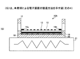
本実施例においては、前記した第5実施例の図8(G)の工程を、図10(G)に示すように変更する。但し、図8(G)以外の工程は、第5実施例と同一である。なお、図中、先に説明した部分には同一の参照符号を付し、説明を省略する。
図10(G)を参照するに、前記中心導体15aおよび15bによって前記誘電体基板12が前記金属筐体11に押し付けられる前に、前記配線板10Aを保持する前記金属筐体11を加熱手段21に載置して、前記加熱手段21により120℃で加熱している。このような加熱工程をさらに設けることで、前記中心導体15aおよび15bによって前記誘電体基板12が前記金属筐体11に押し付けられる前に前記Inシート20が柔らかくなる。そのため、前記した図8(H)および(I)において、前記Inシート20が変形して、当該Inシート20と、前記接地電極19および前記金属筐体11の境界面の接触面積が増加して、当該境界面の電気抵抗と熱抵抗を低減させる効果がさらに大きくなる。
[伝送特性の評価]
次に、本発明による電子装置である高周波デバイスを用いた伝送特性の評価結果を示す。
【0049】
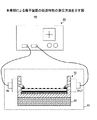
図11は、前記高周波デバイスの伝送特性の測定の方法を示した図である。
【0050】
図11を参照するに、前記高周波デバイスを冷凍機22によって冷却し、さらに真空容器23によって断熱効果を高めて、前記超伝導配線13および前記超伝導接地膜19の抵抗値を十分に下げておく。そこで、ベクトルネットワークアナライザから供給されるパルス波を前記高周波デバイスのIN側から入力し、OUT側からパルス波の波形の乱れを観察する。そこで、前記高周波デバイスを評価したところ、周波数分散は、信号の伝送速度の変化が1%以内に抑えることができたことが確認された。
【0051】
また、その結果、本発明による電子装置である高周波デバイスは、従来用いられていたものに比較して設置面積が約80%と小型化することが可能であり、かつ良好な伝送特性が得られることが確認された
以上、本発明を好ましい実施例について説明したが、本発明は上記の特定の実施例に限定されるものではなく、特許請求の範囲に記載した要旨内において様々な変形・変更が可能である。例えば、本実施例においては、電子装置の例として、高周波の遅延回路を形成する場合を示したが、その他に共振器、フィルタなどの高周波デバイスに対しても適用が可能であり、前記した実施例の場合と同様の効果を得ることが可能である。
[第7実施例]
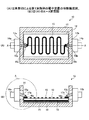
例えば、図12(A)および(B)に、第1実施例の電子装置である高周波デバイス10の変形例である高周波デバイス50を示す。ただし図中、先に説明した部分には同一の参照符号を付し、説明を省略する。
【0052】
図12(A)を参照するに、本実施例は、図1で示した遅延回路を形成する前記超伝導配線13の配線パターンを、超伝導配線53で示すように変更した例である。
【0053】
このように、図2(A)に示した前記超伝導配線13を変更することにより、超伝導配線によって形成されるLC回路を任意に変更して、例えば、共振器、バンドパスフィルタ、ハイパスフィルタなど様々な高周波デバイスを形成することが可能である。図12には、従来用いられている3段ヘアピン型マイクロスプリットフィルタの例を示している。
[第8実施例]
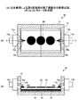
また、図13(A)および(B)に、第1実施例の電子装置である高周波デバイス10の別の変形例である高周波デバイス60を示す。ただし図中、先に説明した部分には同一の参照符号を付し、説明を省略する。
【0054】
図13(A)を参照するに、本実施例は、図2(A)に示した前記超伝導配線13を変更した別の例である。本実施例では、従来用いられている3段ディスクフィルタに本発明を適用した例である。
【0055】
さらに、前記したようなフィルタ、共振気などを組み合わせた高周波デバイスにおいても、本発明を適用することが可能である。
(付記1) 基板の第1の面に第1の配線が形成されると共に、第1の面の反対側に位置する第2の面に第2の配線が配設された電子素子と、
該電子素子を装着する構成とされており、装着状態において前記第2の配線と接続される接地部と、前記第1の配線に接続される接続配線と、前記電子素子を前記電極に向け押圧する押圧手段とを有してなる筐体と
を具備する電子装置であって、
前記押圧手段は、前記接続配線に弾性を持たせ、該接続配線の弾性力により前記電子素子を押圧することにより、前記電子素子を前記接地部に向け押圧する構成であることを特徴とする電子装置。
(付記2) 前記第1の配線および前記第2の配線は超伝導媒体よりなることを特徴とする付記1記載の電子装置。
(付記3) 前記接続配線は、同軸コネクタの中心導体であることを特徴とする付記1または2記載の電子装置。
(付記4) 前記中心導体は、Cu、Be−Cu、りん青銅のいずれかよりなることを特徴とする付記3記載の電子装置。
(付記5) 前記第2の配線と前記接地部の間に、前記第2の配線および前記接地部を電気的に接続する接触媒体を設けたことを特徴とする付記1〜4のうち、いずれか1項記載の電子装置。
(付記6) 前記接触媒体は導電性シートであることを特徴とする付記5記載の電子装置。
(付記7) 前記導電性シートはInシートであることを特徴とする付記6記載の電子装置。
(付記8)前記Inシートの厚さは、0.05〜0.5mmであることを特徴とする付記7記載の電子装置。
(付記9) 前記筐体は、金属からなることを特徴とする付記1〜8のうち、いずれか1項記載の電子装置。
(付記10) 前記第2の配線の上に、前記接触媒体と接触する膜を形成したことを特徴とする付記5〜9のうち、いずれか1項記載の電子装置。
(付記11) 前記基板はMgOよりなることを特徴とする付記1〜10のうち、いずれか1項記載の電子装置。
(付記12) 基板の第1の面に第1の配線が形成されると共に、第1の面の反対側に位置する第2の面に第2の配線が配設された電子素子を、接地部と接続配線を有する筐体に装着する電子装置の製造方法であって、
前記電子素子を前記筐体に載置して前記第2の配線と前記接地部を接続する工程と、
前記接続配線に前記第2の配線を接続する工程と、
前記接続配線の弾性力により前記電子素子を押圧することにより、前記電子素子を前記接地部に向け押圧する工程とを有することを特徴とする電子装置の製造方法。
(付記13) 前記第2の配線と前記接地部の間に、前記第2の配線および前記接地部を電気的に接続する接触媒体を設けたことを特徴とする付記12記載の電子装置。
(付記14) 前記接触媒体を加熱する工程をさらに設けたことを特徴とする付記13記載の電子装置の製造方法。
(付記15) 前記接触媒体はInシートであることを特徴とする付記13または14記載の電子装置の製造方法。
(付記16) 前記第1の配線および前記第2の配線は超伝導媒体よりなることを特徴とする付記12〜15のうち、いずれか1項記載の電子装置の製造方法。
(付記17) 前記配線接続部は同軸コネクタの中心導体であることを特徴とする付記12〜16のうち、いずれか1項記載の電子装置の製造方法。
【0056】
【発明の効果】
本発明によれば、金属筐体に配設された電子装置において、当該電子装置を小型化することにより省スペース化を実現し、かつ当該電子装置の冷却設備への負担を軽減することが可能となった。
【0057】
【図面の簡単な説明】
【図1】(A)および(B)は、従来の電子装置の構成を示す図である。
【図2】(A)は本発明による第1実施例の電子装置の分解構成図、(B)は(A)のX−X断面図である。
【図3】本発明による第1実施例の電子装置の要部拡大図である。
【図4】本発明による第2実施例の電子装置の要部拡大図である。
【図5】本発明による第3実施例の電子装置の要部拡大図である。
【図6】本発明による第4実施例の電子装置の要部拡大図である。
【図7】(A)〜(D)は、本発明による電子装置の製造方法を示す図(その1)である。
【図8】(E)〜(H)は、本発明による電子装置の製造方法を示す図(その2)である。
【図9】(I)〜(J)は、本発明による電子装置の製造方法を示す図(その3)である。
【図10】(G)は、本発明による電子装置の製造方法を示す図(その4)である。
【図11】本発明による電子装置の伝送特性の測定方法を示す図である。
【図12】(A)は本発明による第7実施例の電子装置の分解構成図、(B)は(A)のX−X断面図である。
【図13】(A)は本発明による第8実施例の電子装置の分解構成図、(B)は(A)のX−X断面図である。
【符号の説明】
10,25,35,45,50,60,100 高周波デバイス
10A 配線板
11,101 金属筐体
12,102 誘電体基板
13,53,63,103 超伝導配線
14a,14b,104a,104b 同軸コネクタ
15a,15b,25a,35a,45a,105a,105b 中心導体
16a,16b,106a,106b 配線電極
17a,17b,107a,107b ハンダ
18,108 超伝導接地膜
19,109 接地電極
20,110 Inシート
21 加熱手段
22 冷凍機
23 真空容器
30 ベクトルネットワークアナライザ[0001]
TECHNICAL FIELD OF THE INVENTION
The present invention relates to an electronic device, and more particularly to an electronic device suitable for being applied to a high-frequency device.
[0002]
In recent years, with the explosive spread of wireless communication and the Internet, high-speed and large-capacity transmission technology has become indispensable. For that purpose, a high-quality transmission line for transmitting a high-frequency signal with low loss and less distortion is required.
[0003]
As the high-quality transmission line as described above, for example, it is conceivable to apply a superconductor. The superconductor has a very small surface resistance and a very low phase dispersion in a high frequency region as compared with a normal electrical conductor. Therefore, for example, a micro-split transmission line using a superconductor as a transmission line is very promising as a next-generation transmission technology. In particular, an ultra-high-speed digital circuit or SFQ (Single Flux Quantum, single quantum flux device) It is expected to be applied to wiring of a substrate on which is mounted.
[0004]
However, when the above-described superconductor is used, there is a problem that the load on the cooling means is large because the superconductor must be cooled. For example, the discovery of oxide superconductors has greatly reduced cooling temperature conditions, but still requires cooling to near the boiling point of liquid nitrogen. Therefore, in consideration of practical use, it is important to reduce the burden of cooling as described above.
[0005]
[Prior art]
As an example of a conventionally used electronic device, FIGS. 1A and 1B show a basic structure of a
[0006]
Referring to FIG. 1A, an outline of a high-
[0007]
A
[0008]
Next, FIG. 1B is referred to. However, in the figure, the parts described above are denoted by the same reference numerals, and description thereof will be omitted.
[0009]
A
[0010]
[Patent Document 1]
JP 2001-35598 A
[0011]
[Problems to be solved by the invention]
In order to actually operate the high-
[0012]
However, as described above, the high-
[0013]
Therefore, an object of the present invention is to provide a new and useful electronic device that solves the above-mentioned problems.
[0014]
A specific object of the present invention is to realize space saving by reducing the size of an electronic device including a high-frequency device using a superconductor, and to reduce the thermal load of a cooling facility for cooling the electronic device. It is.
[0015]
[Means for Solving the Problems]
According to the present invention, in order to solve the above-described problems, a first wiring is formed on a first surface of a substrate, and a second wiring is disposed on a second surface opposite to the first surface. An electronic element provided; a grounding section connected to the second wiring in a mounted state; a connection wiring connected to the first wiring; An electronic device comprising: a housing having pressing means for pressing an element toward the electrode, wherein the pressing means makes the connection wiring elastic and the elasticity of the connection wiring makes the connection wiring elastic. An electronic device having a configuration in which the electronic element is pressed toward the ground portion by pressing the electronic element, and the first wiring and the second wiring are made of a superconducting medium. The electronic device is characterized by that.
[0016]
According to the present invention, in the electronic device provided in the housing, the connection element forming a part of a circuit of the electronic device includes the connection element, and the electronic element is connected to the connection element by an elastic force of the connection wiring. Added the function of pressing against the grounding part. As a result, a structure for pressing the electronic element, which has been conventionally required, is not required, and the size of the housing can be reduced to reduce the size of the electronic device, thereby saving space and realizing superconductivity. It is possible to reduce the heat load of the cooling equipment that cools the wiring using the medium.
[0017]
In the present invention, the above problem is solved by forming a first wiring on a first surface of a substrate and arranging a second wiring on a second surface opposite to the first surface. What is claimed is: 1. A method of manufacturing an electronic device, comprising: mounting an electronic element on a housing having a grounding part and a connection wiring, wherein the electronic element is mounted on the housing and the second wiring is connected to the grounding part. Connecting the second wiring to the connection wiring, and pressing the electronic element toward the ground portion by pressing the electronic element by an elastic force of the connection wiring. The problem is solved by a method for manufacturing an electronic device characterized by the following.
[0018]
According to the present invention, in the method of manufacturing an electronic device provided in the housing, the electronic element is attached to the connection wiring forming a part of a circuit of the electronic device by an elastic force of the connection wiring. And a step of pressing against the ground portion. As a result, a structure for pressing the electronic element, which has been conventionally required, becomes unnecessary, and the size of the housing can be reduced to reduce the size of the electronic device, thereby realizing space saving.
[0019]
Therefore, for example, when a superconducting medium is used in an electronic device, it is possible to reduce the load on a cooling facility that cools the superconducting medium.
[0020]
BEST MODE FOR CARRYING OUT THE INVENTION
Next, embodiments of the present invention will be described below with reference to the drawings.
[First embodiment]
2A and 2B are basic structural diagrams of a high-
[0021]
Referring to FIG. 2A, an outline of the high-
[0022]
Next, FIG. 2B is referred to. However, in the figure, the parts described above are denoted by the same reference numerals, and description thereof will be omitted.
[0023]
A
[0024]
In the present embodiment, the
[0025]
For example, in the case of the conventional example shown in FIG. 1A, components such as the
[0026]
FIG. 3 is an enlarged view of a region indicated by A in FIG. However, in the figure, the same reference numerals are given to the previously described portions, and a part of the description is omitted.
[0027]
The
[0028]
In addition, the
[0029]
In addition, the
[0030]
The
[Second embodiment]
FIG. 4 is a modified example of the high-
[0031]
Referring to FIG. 4, in the high-
[Third embodiment]
FIG. 5 shows another modification of the high-
[0032]
Referring to FIG. 5, in the high-
[Fourth embodiment]
FIG. 6 shows still another modification of the high-
[0033]
Referring to FIG. 6, in the present embodiment, the structure is substantially horizontal with the
[Fifth embodiment]
Next, a method for manufacturing a high-frequency device as an electronic device according to the present invention will be described step by step with reference to the drawings.
[0034]
7 (A) to 7 (D), 8 (E) to 8 (H), and 9 (I) to 9 (J) show the flow of the method for manufacturing a high-frequency device according to the present invention. However, in the figure, the same reference numerals are given to the previously described portions, and a part of the description is omitted.
[0035]
First, referring to FIG. 7A, a
[0036]
Next, in FIG. 7B, a superconducting film 13 'made of YBCO is formed on the first side of the
[0037]
Next, in FIG. 7C, the superconducting film 13 'is patterned on a meander having a line width of 0.5 mm by photolithography to form a
[0038]
Next, in FIG. 7D, first, on the first side of the
[0039]
Here, a
[0040]
FIG. 8E is a cross-sectional view of the
[0041]
In FIG. 8F, an In
[0042]
Next, in FIG. 8 (G), the
[0043]
Next, in FIG. 8H,
[0044]
Further, as described above in the description of the first embodiment, the
[0045]
Next, in FIG. 9I, the
[0046]
Next, in FIG. 9 (J), the
[0047]
In the case of the high-
[0048]
Further, the fifth embodiment described above can be modified as in the following sixth embodiment.
[Sixth embodiment]
In the present embodiment, the process of FIG. 8 (G) of the fifth embodiment is changed as shown in FIG. 10 (G). However, steps other than FIG. 8 (G) are the same as in the fifth embodiment. In the figure, the same reference numerals are given to the parts described above, and the description is omitted.
Referring to FIG. 10G, before the
[Evaluation of transmission characteristics]
Next, evaluation results of transmission characteristics using a high-frequency device that is an electronic device according to the present invention will be described.
[0049]
FIG. 11 is a diagram showing a method for measuring the transmission characteristics of the high-frequency device.
[0050]
Referring to FIG. 11, the high-frequency device is cooled by a
[0051]
As a result, the high-frequency device, which is an electronic device according to the present invention, can be reduced in installation area to about 80% as compared with a conventionally used device, and good transmission characteristics can be obtained. Was confirmed
As described above, the present invention has been described with reference to the preferred embodiments. However, the present invention is not limited to the above-described specific embodiments, and various modifications and changes can be made within the scope of the claims. For example, in the present embodiment, a case where a high-frequency delay circuit is formed is shown as an example of the electronic device. However, the present invention is also applicable to a high-frequency device such as a resonator and a filter. The same effect as in the example can be obtained.
[Seventh embodiment]
For example, FIGS. 12A and 12B show a high-
[0052]
Referring to FIG. 12A, the present embodiment is an example in which the wiring pattern of the
[0053]
As described above, by changing the
[Eighth embodiment]
FIGS. 13A and 13B show a high-
[0054]
Referring to FIG. 13A, this embodiment is another example in which the
[0055]
Further, the present invention can be applied to a high-frequency device combining the above-described filter, resonance air, and the like.
(Supplementary Note 1) An electronic element in which a first wiring is formed on a first surface of a substrate and a second wiring is provided on a second surface opposite to the first surface.
The electronic device is configured to be mounted, and in the mounted state, a grounding portion connected to the second wiring, a connection wiring connected to the first wiring, and pressing the electronic device toward the electrode And a housing having pressing means for performing
An electronic device comprising:
The electronic device according to
(Supplementary note 2) The electronic device according to
(Supplementary Note 3) The electronic device according to
(Supplementary note 4) The electronic device according to supplementary note 3, wherein the center conductor is made of any of Cu, Be-Cu, and phosphor bronze.
(Supplementary Note 5) Any of the
(Supplementary note 6) The electronic device according to supplementary note 5, wherein the contact medium is a conductive sheet.
(Supplementary note 7) The electronic device according to supplementary note 6, wherein the conductive sheet is an In sheet.
(Supplementary note 8) The electronic device according to supplementary note 7, wherein the thickness of the In sheet is 0.05 to 0.5 mm.
(Supplementary Note 9) The electronic device according to any one of
(Supplementary Note 10) The electronic device according to any one of Supplementary Notes 5 to 9, wherein a film that contacts the contact medium is formed on the second wiring.
(Supplementary Note 11) The electronic device according to any one of
(Supplementary Note 12) An electronic element having a first wiring formed on a first surface of a substrate and having a second wiring disposed on a second surface opposite to the first surface is grounded. A method for manufacturing an electronic device to be mounted on a housing having a unit and connection wiring,
Mounting the electronic element on the housing and connecting the second wiring and the grounding unit;
Connecting the second wiring to the connection wiring;
Pressing the electronic element toward the ground portion by pressing the electronic element with the elastic force of the connection wiring.
(Supplementary Note 13) The electronic device according to
(Supplementary note 14) The method for manufacturing an electronic device according to
(Supplementary note 15) The method for manufacturing an electronic device according to
(Supplementary note 16) The method of manufacturing an electronic device according to any one of
(Supplementary note 17) The method of manufacturing an electronic device according to any one of
[0056]
【The invention's effect】
ADVANTAGE OF THE INVENTION According to this invention, in the electronic device arrange | positioned at the metal housing | casing, space saving can be implement | achieved by making the said electronic device small-sized, and the burden to the cooling installation of the said electronic device can be reduced. It became.
[0057]
[Brief description of the drawings]
FIGS. 1A and 1B are diagrams showing a configuration of a conventional electronic device.
FIG. 2A is an exploded configuration diagram of the electronic device according to the first embodiment of the present invention, and FIG. 2B is a cross-sectional view taken along line XX of FIG.
FIG. 3 is an enlarged view of a main part of the electronic device according to the first embodiment of the present invention.
FIG. 4 is an enlarged view of a main part of an electronic device according to a second embodiment of the present invention.
FIG. 5 is an enlarged view of a main part of an electronic device according to a third embodiment of the present invention.
FIG. 6 is an enlarged view of a main part of an electronic device according to a fourth embodiment of the present invention.
FIGS. 7A to 7D are diagrams (part 1) illustrating a method of manufacturing an electronic device according to the present invention.
8 (E) to 8 (H) are views (No. 2) showing the method of manufacturing the electronic device according to the present invention.
FIGS. 9A to 9J are views (No. 3) illustrating the method of manufacturing the electronic device according to the present invention.
FIG. 10G is a view (part 4) illustrating the method for manufacturing the electronic device according to the present invention.
FIG. 11 is a diagram illustrating a method for measuring transmission characteristics of an electronic device according to the present invention.
12A is an exploded configuration diagram of an electronic device according to a seventh embodiment of the present invention, and FIG. 12B is a cross-sectional view taken along line XX of FIG.
13A is an exploded configuration diagram of an electronic device according to an eighth embodiment of the present invention, and FIG. 13B is a cross-sectional view taken along line XX of FIG.
[Explanation of symbols]
10,25,35,45,50,60,100 High frequency device
10A wiring board
11,101 metal housing
12,102 dielectric substrate
13,53,63,103 Superconducting wiring
14a, 14b, 104a, 104b Coaxial connector
15a, 15b, 25a, 35a, 45a, 105a, 105b Central conductor
16a, 16b, 106a, 106b Wiring electrode
17a, 17b, 107a, 107b Solder
18,108 Superconducting ground film
19,109 Ground electrode
20,110 In sheet
21 heating means
22 Refrigerator
23 Vacuum container
30 Vector Network Analyzer
Claims (5)
該電子素子を装着する構成とされており、装着状態において前記第2の配線と接続される接地部と、前記第1の配線に接続される接続配線と、前記電子素子を前記電極に向け押圧する押圧手段とを有してなる筐体とを具備する電子装置であって、
前記押圧手段は、前記接続配線に弾性を持たせ、該接続配線の弾性力により前記電子素子を押圧することにより、前記電子素子を前記接地部に向け押圧する構成であることを特徴とする電子装置。An electronic element having a first wiring formed on a first surface of a substrate and having a second wiring disposed on a second surface opposite to the first surface;
The electronic device is configured to be mounted, and in the mounted state, a grounding portion connected to the second wiring, a connection wiring connected to the first wiring, and pressing the electronic device toward the electrode An electronic device comprising: a housing having a pressing means;
The electronic device according to claim 1, wherein the pressing unit presses the electronic element toward the ground portion by providing elasticity to the connection wiring and pressing the electronic element by an elastic force of the connection wiring. apparatus.
前記電子素子を前記筐体に載置して前記第2の配線と前記接地部を接続する工程と、
前記接続配線に前記第1の配線を接続する工程と、
前記接続配線の弾性力により前記電子素子を押圧することにより、前記電子素子を前記接地部に向け押圧する工程とを有することを特徴とする電子装置の製造方法。A first wiring is formed on a first surface of a substrate, and an electronic element having a second wiring disposed on a second surface opposite to the first surface is connected to a grounding portion and a connection wiring. A method for manufacturing an electronic device to be mounted on a housing having
Mounting the electronic element on the housing and connecting the second wiring and the grounding unit;
Connecting the first wiring to the connection wiring;
Pressing the electronic element toward the ground portion by pressing the electronic element with the elastic force of the connection wiring.
Priority Applications (1)
| Application Number | Priority Date | Filing Date | Title |
|---|---|---|---|
| JP2003045967A JP2004259752A (en) | 2003-02-24 | 2003-02-24 | Electronic device and method of manufacturing electronic device |
Applications Claiming Priority (1)
| Application Number | Priority Date | Filing Date | Title |
|---|---|---|---|
| JP2003045967A JP2004259752A (en) | 2003-02-24 | 2003-02-24 | Electronic device and method of manufacturing electronic device |
Publications (1)
| Publication Number | Publication Date |
|---|---|
| JP2004259752A true JP2004259752A (en) | 2004-09-16 |
Family
ID=33112640
Family Applications (1)
| Application Number | Title | Priority Date | Filing Date |
|---|---|---|---|
| JP2003045967A Pending JP2004259752A (en) | 2003-02-24 | 2003-02-24 | Electronic device and method of manufacturing electronic device |
Country Status (1)
| Country | Link |
|---|---|
| JP (1) | JP2004259752A (en) |
Cited By (5)
| Publication number | Priority date | Publication date | Assignee | Title |
|---|---|---|---|---|
| CN100550211C (en) * | 2005-08-31 | 2009-10-14 | 中国科学院物理研究所 | A superconducting filter shielding box with anti-strong vibration function |
| JP2010109403A (en) * | 2008-10-28 | 2010-05-13 | Fujitsu Ltd | Superconducting filter |
| WO2010090657A3 (en) * | 2009-02-05 | 2010-12-23 | Superconductor Technologies, Inc. | Simple efficient assembly and packaging of rf, fdd, tdd, hts and/or cryo-cooled electronic devices |
| JP2022502836A (en) * | 2018-10-02 | 2022-01-11 | インターナショナル・ビジネス・マシーンズ・コーポレーションInternational Business Machines Corporation | Reduced Kapitsa resistance microwave filter for cryogenic environments |
| CN115440879A (en) * | 2022-06-16 | 2022-12-06 | 合肥本源量子计算科技有限责任公司 | Superconducting silicon chip and its preparation method |
-
2003
- 2003-02-24 JP JP2003045967A patent/JP2004259752A/en active Pending
Cited By (7)
| Publication number | Priority date | Publication date | Assignee | Title |
|---|---|---|---|---|
| CN100550211C (en) * | 2005-08-31 | 2009-10-14 | 中国科学院物理研究所 | A superconducting filter shielding box with anti-strong vibration function |
| JP2010109403A (en) * | 2008-10-28 | 2010-05-13 | Fujitsu Ltd | Superconducting filter |
| WO2010090657A3 (en) * | 2009-02-05 | 2010-12-23 | Superconductor Technologies, Inc. | Simple efficient assembly and packaging of rf, fdd, tdd, hts and/or cryo-cooled electronic devices |
| JP2022502836A (en) * | 2018-10-02 | 2022-01-11 | インターナショナル・ビジネス・マシーンズ・コーポレーションInternational Business Machines Corporation | Reduced Kapitsa resistance microwave filter for cryogenic environments |
| US12142804B2 (en) | 2018-10-02 | 2024-11-12 | International Business Machines Corporation | Reduced Kapitza resistance microwave filter for cryogenic environments |
| JP7621245B2 (en) | 2018-10-02 | 2025-01-24 | インターナショナル・ビジネス・マシーンズ・コーポレーション | Reduced Kapitza Resistance Microwave Filters for Cryogenic Environments. |
| CN115440879A (en) * | 2022-06-16 | 2022-12-06 | 合肥本源量子计算科技有限责任公司 | Superconducting silicon chip and its preparation method |
Similar Documents
| Publication | Publication Date | Title |
|---|---|---|
| EP1026772B1 (en) | High-frequency circuit element | |
| JP3924430B2 (en) | Superconducting filter module, superconducting filter, and thermal insulation type coaxial cable | |
| JPWO1995035584A1 (en) | High-frequency circuit elements | |
| JP4236408B2 (en) | Thermal shutdown signal transmission unit and superconducting signal transmission device | |
| Ohshima | High-temperature superconducting passive microwave devices, filters and antennas | |
| JP3866716B2 (en) | filter | |
| JPH07202507A (en) | Micro strip line filter | |
| JP4731515B2 (en) | Tunable filter and manufacturing method thereof | |
| JP3880785B2 (en) | Superconducting filter | |
| KR100714935B1 (en) | Superconducting device | |
| JP2009038567A (en) | Superconducting filter device, superconducting filter package, and superconducting filter device | |
| JP4504932B2 (en) | Superconducting filter device and filter characteristic adjusting method | |
| JP2898462B2 (en) | High frequency filter | |
| JP4587768B2 (en) | Superconducting device and method of manufacturing superconducting device | |
| US20080146450A1 (en) | Superconductor filter unit | |
| JP4061223B2 (en) | Superconducting filter package and superconducting filter device | |
| JP4486551B2 (en) | Superconducting filter device and manufacturing method thereof | |
| JPH05160616A (en) | Thin film resonator | |
| Zhou et al. | Compact superconducting coplanar meander line filters | |
| JP2003110305A (en) | Superconducting filter package and superconducting filter device | |
| JPH05110329A (en) | Superconducting antenna | |
| JPH10224252A (en) | Filter circuit | |
| JP2005354657A (en) | Superconducting filter device | |
| JP2008278225A (en) | Band pass filter and method for manufacturing the same | |
| JP2953338B2 (en) | Superconducting circuit device |
Legal Events
| Date | Code | Title | Description |
|---|---|---|---|
| A621 | Written request for application examination |
Free format text: JAPANESE INTERMEDIATE CODE: A621 Effective date: 20050811 |
|
| A977 | Report on retrieval |
Free format text: JAPANESE INTERMEDIATE CODE: A971007 Effective date: 20070517 |
|
| A131 | Notification of reasons for refusal |
Free format text: JAPANESE INTERMEDIATE CODE: A131 Effective date: 20090616 |
|
| A02 | Decision of refusal |
Free format text: JAPANESE INTERMEDIATE CODE: A02 Effective date: 20091020 |