JP2004247735A - Method for forming local wiring of semiconductor device utilizing selective epitaxial growth - Google Patents
Method for forming local wiring of semiconductor device utilizing selective epitaxial growth Download PDFInfo
- Publication number
- JP2004247735A JP2004247735A JP2004034272A JP2004034272A JP2004247735A JP 2004247735 A JP2004247735 A JP 2004247735A JP 2004034272 A JP2004034272 A JP 2004034272A JP 2004034272 A JP2004034272 A JP 2004034272A JP 2004247735 A JP2004247735 A JP 2004247735A
- Authority
- JP
- Japan
- Prior art keywords
- selective epitaxial
- forming
- epitaxial growth
- local wiring
- gate
- Prior art date
- Legal status (The legal status is an assumption and is not a legal conclusion. Google has not performed a legal analysis and makes no representation as to the accuracy of the status listed.)
- Pending
Links
Images


Classifications
-
- H—ELECTRICITY
- H01—ELECTRIC ELEMENTS
- H01L—SEMICONDUCTOR DEVICES NOT COVERED BY CLASS H10
- H01L21/00—Processes or apparatus adapted for the manufacture or treatment of semiconductor or solid state devices or of parts thereof
- H01L21/02—Manufacture or treatment of semiconductor devices or of parts thereof
- H01L21/04—Manufacture or treatment of semiconductor devices or of parts thereof the devices having at least one potential-jump barrier or surface barrier, e.g. PN junction, depletion layer or carrier concentration layer
- H01L21/18—Manufacture or treatment of semiconductor devices or of parts thereof the devices having at least one potential-jump barrier or surface barrier, e.g. PN junction, depletion layer or carrier concentration layer the devices having semiconductor bodies comprising elements of Group IV of the Periodic System or AIIIBV compounds with or without impurities, e.g. doping materials
- H01L21/28—Manufacture of electrodes on semiconductor bodies using processes or apparatus not provided for in groups H01L21/20 - H01L21/268
-
- H—ELECTRICITY
- H01—ELECTRIC ELEMENTS
- H01L—SEMICONDUCTOR DEVICES NOT COVERED BY CLASS H10
- H01L21/00—Processes or apparatus adapted for the manufacture or treatment of semiconductor or solid state devices or of parts thereof
- H01L21/70—Manufacture or treatment of devices consisting of a plurality of solid state components formed in or on a common substrate or of parts thereof; Manufacture of integrated circuit devices or of parts thereof
- H01L21/71—Manufacture of specific parts of devices defined in group H01L21/70
- H01L21/768—Applying interconnections to be used for carrying current between separate components within a device comprising conductors and dielectrics
- H01L21/76838—Applying interconnections to be used for carrying current between separate components within a device comprising conductors and dielectrics characterised by the formation and the after-treatment of the conductors
- H01L21/76895—Local interconnects; Local pads, as exemplified by patent document EP0896365
-
- H—ELECTRICITY
- H01—ELECTRIC ELEMENTS
- H01L—SEMICONDUCTOR DEVICES NOT COVERED BY CLASS H10
- H01L21/00—Processes or apparatus adapted for the manufacture or treatment of semiconductor or solid state devices or of parts thereof
- H01L21/02—Manufacture or treatment of semiconductor devices or of parts thereof
- H01L21/04—Manufacture or treatment of semiconductor devices or of parts thereof the devices having at least one potential-jump barrier or surface barrier, e.g. PN junction, depletion layer or carrier concentration layer
- H01L21/18—Manufacture or treatment of semiconductor devices or of parts thereof the devices having at least one potential-jump barrier or surface barrier, e.g. PN junction, depletion layer or carrier concentration layer the devices having semiconductor bodies comprising elements of Group IV of the Periodic System or AIIIBV compounds with or without impurities, e.g. doping materials
- H01L21/28—Manufacture of electrodes on semiconductor bodies using processes or apparatus not provided for in groups H01L21/20 - H01L21/268
- H01L21/283—Deposition of conductive or insulating materials for electrodes conducting electric current
- H01L21/285—Deposition of conductive or insulating materials for electrodes conducting electric current from a gas or vapour, e.g. condensation
- H01L21/28506—Deposition of conductive or insulating materials for electrodes conducting electric current from a gas or vapour, e.g. condensation of conductive layers
- H01L21/28512—Deposition of conductive or insulating materials for electrodes conducting electric current from a gas or vapour, e.g. condensation of conductive layers on semiconductor bodies comprising elements of Group IV of the Periodic System
- H01L21/28518—Deposition of conductive or insulating materials for electrodes conducting electric current from a gas or vapour, e.g. condensation of conductive layers on semiconductor bodies comprising elements of Group IV of the Periodic System the conductive layers comprising silicides
-
- H—ELECTRICITY
- H01—ELECTRIC ELEMENTS
- H01L—SEMICONDUCTOR DEVICES NOT COVERED BY CLASS H10
- H01L21/00—Processes or apparatus adapted for the manufacture or treatment of semiconductor or solid state devices or of parts thereof
- H01L21/70—Manufacture or treatment of devices consisting of a plurality of solid state components formed in or on a common substrate or of parts thereof; Manufacture of integrated circuit devices or of parts thereof
- H01L21/77—Manufacture or treatment of devices consisting of a plurality of solid state components or integrated circuits formed in, or on, a common substrate
- H01L21/78—Manufacture or treatment of devices consisting of a plurality of solid state components or integrated circuits formed in, or on, a common substrate with subsequent division of the substrate into plural individual devices
- H01L21/82—Manufacture or treatment of devices consisting of a plurality of solid state components or integrated circuits formed in, or on, a common substrate with subsequent division of the substrate into plural individual devices to produce devices, e.g. integrated circuits, each consisting of a plurality of components
- H01L21/822—Manufacture or treatment of devices consisting of a plurality of solid state components or integrated circuits formed in, or on, a common substrate with subsequent division of the substrate into plural individual devices to produce devices, e.g. integrated circuits, each consisting of a plurality of components the substrate being a semiconductor, using silicon technology
- H01L21/8232—Field-effect technology
- H01L21/8234—MIS technology, i.e. integration processes of field effect transistors of the conductor-insulator-semiconductor type
- H01L21/8238—Complementary field-effect transistors, e.g. CMOS
- H01L21/823871—Complementary field-effect transistors, e.g. CMOS interconnection or wiring or contact manufacturing related aspects
-
- H—ELECTRICITY
- H01—ELECTRIC ELEMENTS
- H01L—SEMICONDUCTOR DEVICES NOT COVERED BY CLASS H10
- H01L21/00—Processes or apparatus adapted for the manufacture or treatment of semiconductor or solid state devices or of parts thereof
- H01L21/02—Manufacture or treatment of semiconductor devices or of parts thereof
- H01L21/02104—Forming layers
- H01L21/02365—Forming inorganic semiconducting materials on a substrate
- H01L21/02367—Substrates
- H01L21/0237—Materials
- H01L21/02373—Group 14 semiconducting materials
- H01L21/02381—Silicon, silicon germanium, germanium
-
- H—ELECTRICITY
- H01—ELECTRIC ELEMENTS
- H01L—SEMICONDUCTOR DEVICES NOT COVERED BY CLASS H10
- H01L21/00—Processes or apparatus adapted for the manufacture or treatment of semiconductor or solid state devices or of parts thereof
- H01L21/02—Manufacture or treatment of semiconductor devices or of parts thereof
- H01L21/02104—Forming layers
- H01L21/02365—Forming inorganic semiconducting materials on a substrate
- H01L21/02518—Deposited layers
- H01L21/02521—Materials
- H01L21/02524—Group 14 semiconducting materials
- H01L21/02532—Silicon, silicon germanium, germanium
-
- H—ELECTRICITY
- H01—ELECTRIC ELEMENTS
- H01L—SEMICONDUCTOR DEVICES NOT COVERED BY CLASS H10
- H01L21/00—Processes or apparatus adapted for the manufacture or treatment of semiconductor or solid state devices or of parts thereof
- H01L21/02—Manufacture or treatment of semiconductor devices or of parts thereof
- H01L21/02104—Forming layers
- H01L21/02365—Forming inorganic semiconducting materials on a substrate
- H01L21/02612—Formation types
- H01L21/02617—Deposition types
- H01L21/0262—Reduction or decomposition of gaseous compounds, e.g. CVD
-
- H—ELECTRICITY
- H01—ELECTRIC ELEMENTS
- H01L—SEMICONDUCTOR DEVICES NOT COVERED BY CLASS H10
- H01L21/00—Processes or apparatus adapted for the manufacture or treatment of semiconductor or solid state devices or of parts thereof
- H01L21/02—Manufacture or treatment of semiconductor devices or of parts thereof
- H01L21/02104—Forming layers
- H01L21/02365—Forming inorganic semiconducting materials on a substrate
- H01L21/02612—Formation types
- H01L21/02617—Deposition types
- H01L21/02636—Selective deposition, e.g. simultaneous growth of mono- and non-monocrystalline semiconductor materials
- H01L21/02639—Preparation of substrate for selective deposition
- H01L21/02645—Seed materials
-
- H—ELECTRICITY
- H01—ELECTRIC ELEMENTS
- H01L—SEMICONDUCTOR DEVICES NOT COVERED BY CLASS H10
- H01L21/00—Processes or apparatus adapted for the manufacture or treatment of semiconductor or solid state devices or of parts thereof
- H01L21/02—Manufacture or treatment of semiconductor devices or of parts thereof
- H01L21/02104—Forming layers
- H01L21/02365—Forming inorganic semiconducting materials on a substrate
- H01L21/02656—Special treatments
- H01L21/02664—Aftertreatments
-
- H—ELECTRICITY
- H01—ELECTRIC ELEMENTS
- H01L—SEMICONDUCTOR DEVICES NOT COVERED BY CLASS H10
- H01L2924/00—Indexing scheme for arrangements or methods for connecting or disconnecting semiconductor or solid-state bodies as covered by H01L24/00
- H01L2924/0001—Technical content checked by a classifier
- H01L2924/0002—Not covered by any one of groups H01L24/00, H01L24/00 and H01L2224/00
Abstract
Description
本発明は、半導体素子の製造方法に係り、特に局部配線を含む半導体素子の製造方法に関する。 The present invention relates to a method for manufacturing a semiconductor device, and more particularly to a method for manufacturing a semiconductor device including local wiring.
半導体素子のサイズ及びデザインルールが漸次縮小されて微細化されることによって素子の集積度が高まっており、半導体素子を構成する重要な要素であるMOSFET(metal oxide semiconductor field effect transistor)のスケールも漸次縮小されている。しかし、MOSFETのスケール縮小はゲート有効チャンネル長さを縮小させてソースとドレーン間のパンチスルー及び短チャンネル効果を誘発させる。このようなパンチスルー及び短チャンネル効果を改善するためにエレベーティッドソース/ドレーン技術が導入されている。また、効率的な回路レイアウトのために局部配線が使われている。 As the size and design rules of a semiconductor device are gradually reduced and miniaturized, the degree of integration of the device is increased, and the scale of a metal oxide semiconductor field effect transistor (MOSFET), which is an important element constituting the semiconductor device, is also gradually increased. Has been reduced. However, scaling down the MOSFET reduces the effective channel length of the gate, causing punch-through between the source and drain and short channel effects. Elevated source / drain technologies have been introduced to improve such punch-through and short channel effects. In addition, local wiring is used for efficient circuit layout.
特許文献1及び特許文献2にエレベーティッドソース/ドレーン及び局部配線の形成方法が開示されている。 Patent Literature 1 and Patent Literature 2 disclose a method of forming an elevated source / drain and local wiring.
特許文献1は、ロードロックLPCVD−Si方法によって露出されたソース/ドレーン領域上には単結晶シリコン膜を、酸化膜及びポリゲート上には多結晶シリコン膜を形成した後、局部配線が形成される領域以外に形成された多結晶シリコン膜をエッチングした後、シリサイド化工程を実施してシリサイド化された局部配線とシリサイド化されたソース/ドレーンとを形成する。 In Patent Literature 1, a local wiring is formed after forming a single crystal silicon film on a source / drain region exposed by a load lock LPCVD-Si method and forming a polycrystalline silicon film on an oxide film and a poly gate. After etching the polycrystalline silicon film formed in the region other than the region, a silicidation process is performed to form silicided local wiring and silicided source / drain.
特許文献2は、ゲート電極を被覆する絶縁膜を形成した後、非晶質シリコン膜を全面に形成し、非晶質シリコン膜をアニーリングして選択的エピタキシャル層を形成した後、局部配線が形成される領域以外の非晶質シリコン膜を除去し、シリサイド化工程を実施してシリサイド化された局部配線とシリサイド化されたソース/ドレーンとを形成する。
ところが、特許文献1では局部配線が形成される領域以外の多結晶シリコンを除去する時、ソース/ドレーン上の単結晶シリコンは損傷させずに多結晶シリコンのみを選択的に除去せねばならず、特許文献2でも局部配線が形成される領域以外の非晶質シリコンを除去する時、ソース/ドレーン上の単結晶シリコンは損傷させずに非晶質シリコンのみを選択的に除去せねばならない。 However, according to Patent Document 1, when removing polycrystalline silicon other than the region where the local wiring is formed, it is necessary to selectively remove only the polycrystalline silicon without damaging the monocrystalline silicon on the source / drain. Also in Patent Document 2, when removing amorphous silicon other than the region where the local wiring is formed, it is necessary to selectively remove only the amorphous silicon without damaging the single crystal silicon on the source / drain.
しかし、現実的に、単結晶シリコンを損傷させずに多結晶シリコンまたは非晶質シリコンのみを選択的に除去することが難しいために前記特許に開示されている方法適用に限界がある。 However, in practice, it is difficult to selectively remove only polycrystalline silicon or amorphous silicon without damaging single-crystal silicon, so that the method disclosed in the above patent is limited in application.
本発明が解決しようとする技術的課題は、単純化されて適用が容易である局部配線を含む半導体素子の製造方法を提供しようとするところにある。 A technical problem to be solved by the present invention is to provide a method of manufacturing a semiconductor device including a local wiring, which is simplified and easily applied.
前記技術的課題を達成するために、本発明による局部配線を含む半導体素子の製造方法によれば、局部配線が形成される半導体基板上の領域であって選択的エピタキシャル成長シード層のない領域上に選択的エピタキシャル成長シード層パターンを形成する。次いで、選択的エピタキシャル成長を実施し、形成された選択的エピタキシャル層の抵抗を下げて局部配線を完成する。 In order to achieve the above technical object, according to a method for manufacturing a semiconductor device including a local wiring according to the present invention, a method for manufacturing a semiconductor device including a local wiring is performed on a region on a semiconductor substrate where a local wiring is formed without a selective epitaxial growth seed layer. A selective epitaxial growth seed layer pattern is formed. Next, selective epitaxial growth is performed to reduce the resistance of the formed selective epitaxial layer to complete the local wiring.
その他の実施の形態の具体的な事項は詳細なる説明及び図面に含まれている。 Specific items of other embodiments are included in the detailed description and drawings.
本発明によれば、単純で、かつ容易な方法で局部配線が形成できる。また、局部配線の形成と共にエレベーティッドソース/ドレーンを同時に形成することによってトランジスタのパンチスルー及び短チャンネル効果が改善できる。 According to the present invention, local wiring can be formed by a simple and easy method. Also, by forming the elevated source / drain simultaneously with the formation of the local wiring, the punch-through and short channel effect of the transistor can be improved.
以下、添付した図面を参照して本発明による局部配線を含む半導体素子の製造方法に関する実施の形態を説明する。しかし、本発明は以下で開示される実施の形態に限定されるものでなく相異なる多様な形態で具現され、ただ本実施の形態は本発明の開示を完全にし、当業者に発明の範疇を完全に知らせるために提供されるものであり、本発明は特許請求の範囲によって定義されるのみである。図面で各層及び物質の形態及び厚さは説明の便宜のために誇張または概略化されたものである。明細書全体にかけて同一参照符号は同一部材を指す。 Hereinafter, an embodiment of a method for manufacturing a semiconductor device including local wiring according to the present invention will be described with reference to the accompanying drawings. However, the present invention is not limited to the embodiments disclosed below, but may be embodied in various different forms. However, the present embodiments complete the disclosure of the present invention, and those skilled in the art will recognize the scope of the present invention. It is provided for complete notification and the invention is only defined by the appended claims. In the drawings, the form and thickness of each layer and material are exaggerated or simplified for convenience of description. Like reference numerals refer to like members throughout the specification.
以下、本実施の形態では局部配線を含む半導体素子の一例として、SRAM(Static Random Access Memory)を例に挙げて説明する。SRAMの場合、局部配線は隣接するトランジスタ間のソース/ドレーンを連結するか、隣接するトランジスタ間のソース/ドレーンとゲートとを連結するために使われる配線を指す。 Hereinafter, in this embodiment, an SRAM (Static Random Access Memory) will be described as an example of a semiconductor element including a local wiring. In the case of an SRAM, a local line refers to a line used to connect a source / drain between adjacent transistors or to connect a source / drain and a gate between adjacent transistors.
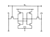
図1は、完全CMOS SRAMの等価回路図である。完全CMOS SRAMの1セルは2個のPMOSトランジスタと4個のNMOSトランジスタで構成される。完全CMOS SRAMは工程が単純であり、スタンバイ電流が少なく、低電圧動作が可能であり、ソフトエラー耐性がよく、多様なモバイル機器、多様なディスクドライバなどに広く使われる。図1で、WLは、ワードラインを、BL及び/BLは、ビットラインを、VCCラインは、電源電圧ラインを、VSSラインは、グラウンドラインをそれぞれ指す。 FIG. 1 is an equivalent circuit diagram of a complete CMOS SRAM. One cell of the complete CMOS SRAM is composed of two PMOS transistors and four NMOS transistors. The complete CMOS SRAM has a simple process, low standby current, low-voltage operation, good soft error resistance, and is widely used in various mobile devices and various disk drivers. In FIG. 1, WL indicates a word line, BL and / BL indicate a bit line, a VCC line indicates a power supply voltage line, and a VSS line indicates a ground line.
図2は、図1の完全CMOS SRAMを製造するための活性領域パターン、ゲート電極パターン及び各配線を同時に示すレイアウトである。点線で表示された矩形が1セルを限定する。110は、活性領域パターンを、120は、ゲートパターンを、LI1とLI3は、トランジスタのソース/ドレーンと隣接トランジスタのソース/ドレーンとを連結するための局部配線を、LI2とLI4は、トランジスタのソース/ドレーンと隣接トランジスタのゲートとを連結するための局部配線をそれぞれ指す。 FIG. 2 is a layout showing simultaneously an active region pattern, a gate electrode pattern, and each wiring for manufacturing the complete CMOS SRAM of FIG. The rectangle indicated by the dotted line limits one cell. 110 is an active region pattern, 120 is a gate pattern, LI1 and LI3 are local wirings for connecting the source / drain of the transistor and the source / drain of the adjacent transistor, and LI2 and LI4 are the source of the transistor. / A local wiring for connecting the drain and the gate of the adjacent transistor.
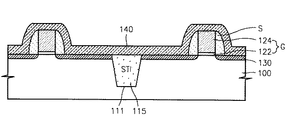
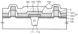
図3ないし図7は、トランジスタのソース/ドレーンと隣接トランジスタのソース/ドレーンとを連結するための局部配線LI1、LI3を製造する方法を説明するための断面図である。 3 to 7 are cross-sectional views illustrating a method of manufacturing local interconnects LI1 and LI3 for connecting a source / drain of a transistor and a source / drain of an adjacent transistor.
図3を参照すれば、活性領域パターン(図2の110)を定義するマスクを使用して半導体基板100をパターニングして浅いトレンチ素子分離領域STIを形成する。まず、半導体基板100を300Åないし10000Å深さにエッチングしてトレンチ111を形成する。次いで、トレンチ111を形成するためのドライエッチング工程によって半導体基板100が受けた損傷を回復させるために熱処理工程を実施して熱酸化膜(図示せず)を形成する。次に、ストレス緩衝膜で窒化膜ライナー(図示せず)を40ないし50Å厚さに形成した後、トレンチ111内部を絶縁膜115で埋め込んだ後、絶縁膜115の膜質を細かくするための熱処理工程を実施する。次いで、絶縁膜を化学機械的ポリシング工程またはエッチバッグ工程で平坦化してSTIを完成して活性領域を定義する。
Referring to FIG. 3, the
次いで、STIによって定義された活性領域上にゲート酸化膜122及びポリシリコン膜124を順に積層した後、ゲートパターン(図2の120)が定義されているマスクを使用してポリシリコン膜124及びゲート酸化膜122をパターニングしてゲートGを形成する。次いで、LDD(lightly doped drain)領域130形成のためのイオン注入を実施した後、ゲートG側壁に絶縁スペーサSを形成する。LDD領域形成のためのイオン注入はヒ素イオンを1014ないし1015濃度で20ないし40KeVで注入して実施する。次いで、結果物全面に選択的エピタキシャル成長シード層140を形成する。選択的エピタキシャル成長シード層140としては、SixOyNz層が形成できる。SixOyNz膜の場合、効果的なシード層として作用するためにはxは、55、yは、15、zは、30であることが望ましい。
Next, after a
図4を参照すれば、選択的エピタキシャル成長シード層140(図3参照)をパターニングして局部配線が形成されねばならないが、選択的エピタキシャル成長シード層のない絶縁領域、例えば、STI領域上にのみ選択的エピタキシャル成長シード層パターン140Pを形成する。 Referring to FIG. 4, the selective epitaxial growth seed layer 140 (see FIG. 3) must be patterned to form a local interconnect, but only selectively on an insulating region without the selective epitaxial growth seed layer, for example, an STI region. An epitaxial growth seed layer pattern 140P is formed.
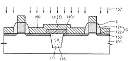
次いで、選択的エピタキシャル層150を形成する。真空チャンバ内に基板100をローディングした後、チャンバ内の温度を850ないし950℃とし、Siソースガス、例えば、SiH4またはSi2H6ガスを1分ないし2分間供給すれば、活性領域を構成するシリコン基板100、選択的エピタキシャル成長シード層パターン140P上部及びゲートG上部にのみ選択的エピタキシャル層150が形成され、絶縁スペーサS上には選択的エピタキシャル層が形成されない。次いで、選択的エピタキシャル層150の抵抗を下げて導電性を帯びせるようにするためのイオン注入155を実施して局部配線LI1、LI3(図2参照)を形成する。イオン注入155はリンイオンを1012ないし1013濃度で20ないし50KeVで注入するか、ヒ素イオンを1014ないし1015濃度で20ないし40KeVで注入する。
Next, a selective
次いで、図5に示されているように、ソース/ドレーン領域形成のためのイオン注入157を実施する。イオン注入157はヒ素イオンを1014ないし1015濃度で20ないし40KeVで注入する。
Next, as shown in FIG. 5,
図6を参照すれば、基板100全面に高融点金属層160を形成する。高融点金属としては、コバルト(Co)、チタン(Ti)、ニッケル(Ni)、白金(Pt)、タングステン(W)、モリブデン(Mo)などが挙げられる。
Referring to FIG. 6, a
次いで、図7に示されているように、多様な急速熱処理(Rapid Thermal Annealing:RTA)を通じてシリサイド化を進行した後、未反応の高融点金属層160を除去する。その結果、シリサイド化されたソース/ドレーンを連結する局部配線LI1、LI3とシリサイド化されたゲートとを完成する。シリサイド化によって局部配線LI1、LI3の抵抗をより効果的に下げられる。
Next, as shown in FIG. 7, after performing silicidation through various rapid thermal annealing (RTA), the unreacted
本実施の形態では、ソース/ドレーン形成のためのイオン注入157を選択的エピタキシャル層150を形成した後に行ったが、イオン注入157は選択的エピタキシャル層150形成前後のいつでも可能である。例えば、ゲートG側壁に絶縁スペーサSを形成した直後にソース/ドレーン形成のためのイオン注入157を行うこともできる。
In this embodiment, the
また、本実施の形態では選択的エピタキシャル層にイオン注入してシリサイド化して局部配線LI1、LI3を完成したが、選択的エピタキシャル層へのイオン注入のみでも局部配線として使用でき、イオン注入なしにシリサイド化することだけでも局部配線として使用できる。 In this embodiment, the local wirings LI1 and LI3 are completed by ion implantation into the selective epitaxial layer and silicidation is completed. However, the ion implantation into the selective epitaxial layer alone can be used as the local wiring, and the silicide can be used without ion implantation. Can be used as local wiring.
図8ないし図10は、トランジスタのソース/ドレーンと隣接トランジスタのゲートとを連結するための局部配線LI2、LI4を製造する方法を説明するための断面図である。隣接するトランジスタのソース/ドレーンを連結するための局部配線LI1、LI3の製造方法と同じ工程についてはその説明を省略する。 8 to 10 are cross-sectional views illustrating a method of manufacturing local interconnects LI2 and LI4 for connecting a source / drain of a transistor and a gate of an adjacent transistor. Descriptions of the same steps as those in the method of manufacturing the local wirings LI1 and LI3 for connecting the source / drain of the adjacent transistor are omitted.
図8を参照すれば、STI、ゲートG及び側壁スペーサSが形成されている半導体基板100全面に絶縁膜を形成した後、これをパターニングしてトランジスタのソース/ドレーンと隣接トランジスタのゲートGとを露出させる絶縁膜パターン128Pを形成する。次いで、絶縁膜パターン128Pが形成されている基板100全面に選択的エピタキシャル成長シード層140を形成する。選択的エピタキシャル成長シード層140としては、SixOyNz層が形成できる。SixOyNz膜の場合、効果的なシード層として作用するためにはxは55、yは15、zは30であることが望ましい。
Referring to FIG. 8, after an insulating film is formed on the entire surface of the
図9を参照すれば、選択的エピタキシャル成長シード層140(図8参照)をパターニングして絶縁膜パターン128P上に選択的エピタキシャル成長シード層パターン140Pを形成する。 Referring to FIG. 9, the selective epitaxial growth seed layer 140 (see FIG. 8) is patterned to form the selective epitaxial growth seed layer pattern 140P on the insulating layer pattern 128P.
次いで、図10に示されているように活性領域を構成するシリコン基板100、選択的エピタキシャル成長シード層パターン140P上部及び露出されたゲートG上部に選択的エピタキシャル層を形成した後、この抵抗を下げてトランジスタのゲートとこれと隣接したトランジスタのソース/ドレーンとを連結する局部配線LI2、LI4を形成する。エピタキシャル層の抵抗を下げる方法としては、適切なイオン注入、シリサイド化またはこれらの組合せが使用できる。
Next, as shown in FIG. 10, a selective epitaxial layer is formed on the
以上、トランジスタのソース/ドレーンと隣接トランジスタのソース/ドレーンとを連結する局部配線LI1、LI3を形成する実施の形態とトランジスタのソース/ドレーンと隣接トランジスタのゲートとを連結する局部配線LI2、LI4を形成する実施の形態とを別々に述べたが、これらを適切に結合して最も単純化された工程でSRAM素子の局部配線LI1ないしLI4を形成するのに使用できることは当業者に自明である。 As described above, the embodiment in which the local lines LI1 and LI3 connecting the source / drain of the transistor and the source / drain of the adjacent transistor are formed, and the local lines LI2 and LI4 connecting the source / drain of the transistor and the gate of the adjacent transistor are formed. Although the embodiments to be formed are described separately, it is obvious to those skilled in the art that these can be appropriately combined and used to form the local wirings LI1 to LI4 of the SRAM device in the simplest process.
以上、本発明を望ましい実施の形態を挙げて詳細に述べたが、本発明は前記実施の形態に限定されず、各膜の厚さ、サイズ、構成物質、これらの形成方法などは本発明の技術的思想内で当業者によって様々な変形が可能であることは当然である。 As described above, the present invention has been described in detail with reference to the preferred embodiments. However, the present invention is not limited to the above-described embodiments, and the thickness, size, constituent materials, forming methods, and the like of each film are not limited to those of the present invention. Naturally, various modifications can be made by those skilled in the art within the technical concept.
本発明は半導体素子の製造に利用される。特に、本発明は局部配線の形成と共にエレベーティッドソース/ドレーンを同時に形成できるためにトランジスタのパンチスルー及び短チャンネル効果が改善された半導体素子が製造できる。 INDUSTRIAL APPLICATION This invention is utilized for manufacture of a semiconductor element. In particular, according to the present invention, the elevated source / drain can be formed simultaneously with the formation of the local wiring, so that a semiconductor device with improved transistor punch-through and short channel effect can be manufactured.
100 半導体基板
111 トレンチ
115 絶縁膜
122 ゲート酸化膜
124 ポリシリコン膜
G ゲート
130 LDD領域
140 選択的エピタキシャル成長シード層
150 選択的エピタキシャル層
155 イオン注入
S 絶縁スペーサ
STI トレンチ素子分離領域
REFERENCE SIGNS
Claims (8)
前記結果物に対して選択的エピタキシャル成長を実施して選択的エピタキシャル層を形成する段階と、
前記選択的エピタキシャル層の抵抗を下げて前記局部配線として完成する段階と、を含むことを特徴とする局部配線を含む半導体素子の製造方法。 Forming a selective epitaxial growth seed layer pattern on a region on the semiconductor substrate where the local wiring is to be formed and without the selective epitaxial growth seed layer;
Performing a selective epitaxial growth on the resultant to form a selective epitaxial layer;
Lowering the resistance of the selective epitaxial layer to complete the local wiring, and manufacturing the semiconductor device including the local wiring.
前記半導体基板に浅いトレンチ素子分離領域を形成して活性領域を定義する段階と、
前記活性領域上にそれぞれゲートを形成する段階と、
前記ゲート側壁にスペーサを形成する段階と、をさらに具備し、
前記選択的エピタキシャル成長シード層パターンを形成する段階は、
前記浅いトレンチ素子分離領域上に前記選択的エピタキシャル成長シード層パターンを形成する段階であり、
前記選択的エピタキシャル層を形成する段階は、
前記活性領域、前記選択的エピタキシャル成長シード層パターン、及び前記ゲート上に前記選択的エピタキシャル層を形成する段階であり、
前記局部配線はトランジスタのソース/ドレーンと隣接トランジスタのソース/ドレーンとを連結する局部配線であることを特徴とする請求項1に記載の局部配線を含む半導体素子の製造方法。 Before the step of forming the selective epitaxial growth seed layer pattern,
Forming an active region by forming a shallow trench isolation region in the semiconductor substrate;
Forming a gate on each of the active regions;
Forming a spacer on the gate side wall;
The step of forming the selective epitaxial growth seed layer pattern includes:
Forming the selective epitaxial growth seed layer pattern on the shallow trench isolation region;
The step of forming the selective epitaxial layer includes:
Forming the selective epitaxial layer on the active region, the selective epitaxial growth seed layer pattern, and the gate;
2. The method of claim 1, wherein the local wiring is a local wiring connecting a source / drain of a transistor and a source / drain of an adjacent transistor.
前記半導体基板に浅いトレンチ素子分離領域を形成して活性領域を定義する段階と、
前記活性領域上に相互隣接した第1及び第2ゲートを形成する段階と、
前記第1及び第2ゲート側壁にスペーサを形成する段階と、
前記第1ゲートが形成されている活性領域と前記第2ゲートとを露出させる絶縁膜パターンとを形成する段階と、をさらに具備し、
前記選択的エピタキシャル成長シード層パターンを形成する段階は、
前記絶縁膜パターン上に前記選択的エピタキシャル成長シード層パターンを形成する段階であり、
前記選択的エピタキシャル層を形成する段階は、
前記第1ゲートが形成されている活性領域、前記選択的エピタキシャル成長シード層パターン、及び前記第2ゲート上に前記選択的エピタキシャル層を形成する段階であり、
前記局部配線はトランジスタのソース/ドレーンと隣接トランジスタのゲートとを連結する局部配線であることを特徴とする請求項1に記載の局部配線を含む半導体素子の製造方法。 Before the step of forming the selective epitaxial growth seed layer pattern,
Forming an active region by forming a shallow trench isolation region in the semiconductor substrate;
Forming first and second gates adjacent to each other on the active region;
Forming spacers on the first and second gate sidewalls;
Forming an insulating layer pattern exposing the active region in which the first gate is formed and the second gate; and
The step of forming the selective epitaxial growth seed layer pattern includes:
Forming the selective epitaxial growth seed layer pattern on the insulating film pattern;
The step of forming the selective epitaxial layer includes:
Forming an active region where the first gate is formed, the selective epitaxial growth seed layer pattern, and the selective epitaxial layer on the second gate;
2. The method according to claim 1, wherein the local wiring is a local wiring connecting a source / drain of a transistor and a gate of an adjacent transistor.
前記選択的エピタキシャル層にイオンを注入して抵抗を下げる段階であることを特徴とする請求項1ないし請求項3のうち何れか1項に記載の局部配線を含む半導体素子の製造方法。 The step of lowering the resistance of the selective epitaxial layer and completing the local wiring includes:
4. The method according to claim 1, further comprising the step of implanting ions into the selective epitaxial layer to reduce the resistance.
前記選択的エピタキシャル層をシリサイド化して抵抗を下げる段階であることを特徴とする請求項1ないし請求項3のうち何れか1項に記載の局部配線を含む半導体素子の製造方法。 The step of lowering the resistance of the selective epitaxial layer and completing the local wiring includes:
4. The method according to claim 1, wherein the selective epitaxial layer is silicided to reduce the resistance.
前記選択的エピタキシャル層にイオンを注入する段階と、
前記選択的エピタキシャル層をシリサイド化する段階と、を含むことを特徴とする請求項1ないし請求項3のうち何れか1項に記載の局部配線を含む半導体素子の製造方法。 The step of lowering the resistance of the selective epitaxial layer and completing the local wiring includes:
Implanting ions into the selective epitaxial layer;
4. The method as claimed in claim 1, further comprising the step of silicidizing the selective epitaxial layer.
Applications Claiming Priority (1)
| Application Number | Priority Date | Filing Date | Title |
|---|---|---|---|
| KR10-2003-0009139A KR100493047B1 (en) | 2003-02-13 | 2003-02-13 | Fabrication method of local interconnection using selective epitaxial growth |
Publications (1)
| Publication Number | Publication Date |
|---|---|
| JP2004247735A true JP2004247735A (en) | 2004-09-02 |
Family
ID=33028805
Family Applications (1)
| Application Number | Title | Priority Date | Filing Date |
|---|---|---|---|
| JP2004034272A Pending JP2004247735A (en) | 2003-02-13 | 2004-02-10 | Method for forming local wiring of semiconductor device utilizing selective epitaxial growth |
Country Status (3)
| Country | Link |
|---|---|
| US (1) | US7049218B2 (en) |
| JP (1) | JP2004247735A (en) |
| KR (1) | KR100493047B1 (en) |
Cited By (3)
| Publication number | Priority date | Publication date | Assignee | Title |
|---|---|---|---|---|
| KR100653853B1 (en) * | 2005-05-24 | 2006-12-05 | 네오폴리((주)) | Method for Crystallizing Amorphous Semiconductor Thin Film by Epitaxy Growth Using Non-metal Seed and Method for Fabricating Poly Crystalline Thin Film Transistor |
| JP2013546158A (en) * | 2010-09-06 | 2013-12-26 | ユ−ジーン テクノロジー カンパニー.リミテッド | Manufacturing method of semiconductor device |
| CN107017256A (en) * | 2016-01-15 | 2017-08-04 | 台湾积体电路制造股份有限公司 | Local interlinkage part and its manufacture method in semiconductor devices |
Families Citing this family (3)
| Publication number | Priority date | Publication date | Assignee | Title |
|---|---|---|---|---|
| US8983241B2 (en) | 2010-12-22 | 2015-03-17 | Bing Li | Optical waveguide switch |
| US9178085B2 (en) | 2010-12-22 | 2015-11-03 | Bing Li | Waveguide photodetector and forming method thereof |
| US9256028B2 (en) | 2011-01-14 | 2016-02-09 | Bing Li | Dispersion-corrected arrayed waveguide grating |
Citations (4)
| Publication number | Priority date | Publication date | Assignee | Title |
|---|---|---|---|---|
| JPH1187266A (en) * | 1997-09-09 | 1999-03-30 | Oki Electric Ind Co Ltd | Fabrication of semiconductor device |
| JP2000114262A (en) * | 1998-10-05 | 2000-04-21 | Toshiba Corp | Semiconductor device and its manufacture |
| JP2001217319A (en) * | 2000-02-04 | 2001-08-10 | Hitachi Ltd | Semiconductor integrated circuit device and manufacturing method therefor |
| JP2003197768A (en) * | 2001-12-25 | 2003-07-11 | Toshiba Corp | Semiconductor device and its manufacturing method |
Family Cites Families (4)
| Publication number | Priority date | Publication date | Assignee | Title |
|---|---|---|---|---|
| US5166771A (en) * | 1990-01-12 | 1992-11-24 | Paradigm Technology, Inc. | Self-aligning contact and interconnect structure |
| US5118639A (en) * | 1990-05-29 | 1992-06-02 | Motorola, Inc. | Process for the formation of elevated source and drain structures in a semiconductor device |
| US5893741A (en) * | 1997-02-07 | 1999-04-13 | National Science Council | Method for simultaneously forming local interconnect with silicided elevated source/drain MOSFET's |
| EP1280189A1 (en) * | 2001-07-16 | 2003-01-29 | Alcatel | Process for selective epitaxial growth and bipolar transistor made by using such process |
-
2003
- 2003-02-13 KR KR10-2003-0009139A patent/KR100493047B1/en not_active IP Right Cessation
-
2004
- 2004-01-28 US US10/766,645 patent/US7049218B2/en not_active Expired - Fee Related
- 2004-02-10 JP JP2004034272A patent/JP2004247735A/en active Pending
Patent Citations (4)
| Publication number | Priority date | Publication date | Assignee | Title |
|---|---|---|---|---|
| JPH1187266A (en) * | 1997-09-09 | 1999-03-30 | Oki Electric Ind Co Ltd | Fabrication of semiconductor device |
| JP2000114262A (en) * | 1998-10-05 | 2000-04-21 | Toshiba Corp | Semiconductor device and its manufacture |
| JP2001217319A (en) * | 2000-02-04 | 2001-08-10 | Hitachi Ltd | Semiconductor integrated circuit device and manufacturing method therefor |
| JP2003197768A (en) * | 2001-12-25 | 2003-07-11 | Toshiba Corp | Semiconductor device and its manufacturing method |
Cited By (6)
| Publication number | Priority date | Publication date | Assignee | Title |
|---|---|---|---|---|
| KR100653853B1 (en) * | 2005-05-24 | 2006-12-05 | 네오폴리((주)) | Method for Crystallizing Amorphous Semiconductor Thin Film by Epitaxy Growth Using Non-metal Seed and Method for Fabricating Poly Crystalline Thin Film Transistor |
| JP2013546158A (en) * | 2010-09-06 | 2013-12-26 | ユ−ジーン テクノロジー カンパニー.リミテッド | Manufacturing method of semiconductor device |
| CN107017256A (en) * | 2016-01-15 | 2017-08-04 | 台湾积体电路制造股份有限公司 | Local interlinkage part and its manufacture method in semiconductor devices |
| KR101810319B1 (en) * | 2016-01-15 | 2017-12-18 | 타이완 세미콘덕터 매뉴팩쳐링 컴퍼니 리미티드 | Method for fabricating a local interconnect in a semiconductor device |
| US9881872B2 (en) | 2016-01-15 | 2018-01-30 | Taiwan Semiconductor Manufacturing Co., Ltd. | Method for fabricating a local interconnect in a semiconductor device |
| US10157845B2 (en) | 2016-01-15 | 2018-12-18 | Taiwan Semiconductor Manufacturing Co., Ltd. | Method for fabricating a local interconnect in a semiconductor device |
Also Published As
| Publication number | Publication date |
|---|---|
| US7049218B2 (en) | 2006-05-23 |
| KR20040073154A (en) | 2004-08-19 |
| US20040209454A1 (en) | 2004-10-21 |
| KR100493047B1 (en) | 2005-06-07 |
Similar Documents
| Publication | Publication Date | Title |
|---|---|---|
| US20210313467A1 (en) | Semiconductor device including gate electrode for applying tensile stress to silicon substrate, and method of manufacturing the same | |
| US10840374B2 (en) | Semiconductor devices with shaped portions of elevated source/drain regions | |
| US7666748B2 (en) | Method of forming amorphous source/drain extensions | |
| US5998849A (en) | Semiconductor device having highly-doped source/drain regions with interior edges in a dislocation-free state | |
| US20030102518A1 (en) | Finfet SRAM cell using low mobility plane for cell stability and method for forming | |
| JP2004214628A (en) | Cmos device and manufacturing device thereof | |
| JP2002329864A (en) | Semiconductor device and its manufacturing method | |
| KR20100081667A (en) | Semiconductor devices having strained channels and methods of manufacturing the same | |
| JP2004527127A (en) | Method for performing accelerated oxidation of MOS transistor gate corner | |
| TW200414321A (en) | Method for fabricating semiconductor device | |
| KR100493047B1 (en) | Fabrication method of local interconnection using selective epitaxial growth | |
| CN108573873A (en) | The manufacturing method of semiconductor devices | |
| US20080003751A1 (en) | Methods for forming dual poly gate of semiconductor device | |
| US6180474B1 (en) | Method for fabricating semiconductor device | |
| KR100549001B1 (en) | fabrication method of a MOS transistor having a total silicide gate | |
| JP2003007878A (en) | Manufacturing method of flash memory and transistor | |
| JPH07135313A (en) | Fet transistor and its fabrication | |
| EP0923114B1 (en) | Process for self-aligned implantation | |
| KR100608324B1 (en) | Method of manufacture semiconductor device | |
| JP2004128182A (en) | Semiconductor integrated circuit device and its manufacturing method | |
| KR20080096076A (en) | Semiconductor device and method of fabricating the same | |
| KR20030044144A (en) | Method of manufacturing a semiconductor device | |
| JP2004022813A (en) | Semiconductor device and its manufacturing method | |
| JPH07142715A (en) | Production of semiconductor device | |
| JP2009141295A (en) | Method of manufacturing semiconductor apparatus |
Legal Events
| Date | Code | Title | Description |
|---|---|---|---|
| A621 | Written request for application examination |
Free format text: JAPANESE INTERMEDIATE CODE: A621 Effective date: 20070124 |
|
| A977 | Report on retrieval |
Free format text: JAPANESE INTERMEDIATE CODE: A971007 Effective date: 20091019 |
|
| A131 | Notification of reasons for refusal |
Free format text: JAPANESE INTERMEDIATE CODE: A131 Effective date: 20100914 |
|
| A521 | Request for written amendment filed |
Free format text: JAPANESE INTERMEDIATE CODE: A523 Effective date: 20101119 |
|
| A02 | Decision of refusal |
Free format text: JAPANESE INTERMEDIATE CODE: A02 Effective date: 20110118 |